Fano resonance from a one-dimensional topological photonic crystal
An ultra-compact one-dimensional topological photonic crystal (1D-TPC) is designed in a single mode silicon bus-waveguide to generate Fano resonance lineshape. The Fano resonance comes from the interference between the discrete topological boundary state of the 1D-TPC and the continuum high-order leaky mode of the bus-waveguide. Standalone asymmetric Fano resonance lineshapes are obtained experimentally in the waveguide transmission spectrum with a maximum extinction ratio of 33 dB and a slope ratio of 10 dB/nm over a broadband flat background.
I Introduction
Constructive and destructive interferences between localized discrete state and continuum state usually give rise to asymmetric spectra, which is known as Fano resonance Fano (1961). Asymmetric lineshape of Fano resonance exhibits an ultra-sharp variation from the minimum to the maximum compared to the symmetric Lorenzian lineshape with an approximative quality () factor Yu et al. (2016). This steeper resonant peak provides great advantages for chip-scale integrated applications like low-threshold lasing Limonov et al. (2017); Yu et al. (2017), high-sensitivity optical sensing Yi, Citrin, and Zhou (2010); Tu et al. (2017); Zhang et al. (2020a) and low-power all-optical switching Yu et al. (2016); Nozaki et al. (2013); Yu et al. (2014); Heuck et al. (2013). Thanks to the maturity and rapid development of planar processing technology, a large number of structures such as microring resonators Zhang, Li, and Yao (2016); Qiu et al. (2012); Gu et al. (2019, 2020); Fang et al. (2020), microdisks Li et al. (2012) and photonic crystal (PC) nano-cavitiesYu et al. (2016, 2017); Nozaki et al. (2013); Yu et al. (2014); Heuck et al. (2013) have been proposed to generate the Fano resonance. Among them, more compact designs are always expected to meet the rapid development of large-scale photonic integrated circuits.
Recently, topological photonics attracted remarkable attention due to its unique properties and made great progress especially when it is combined with the mature CMOS-compatible platforms. Photonic analogues of topological quantum systems can be easily realized via PC or microring arrays Raghu and Haldane (2008); Chen et al. (2017); Khanikaev and Shvets (2017), which promise a new generation of compact chip-scale photonic devices. For example, topological boundary states (TBSs) existing in open bandgaps of PCs become the focus in building high factor nano-cavities Ota et al. (2018); Zhang et al. (2020b); Shao et al. (2020); Han et al. (2019). A topology-based design of zero-dimensional interface state in a one-dimensional (1D) PC nanobeam guarantees the existence of only one cavity mode within its photonic bandgap Ota et al. (2018). This special design takes advantage of highly localized mode in an ultra-small volume with a high energy density in the nano-cavity. In addition, a dislocation-based topological cavity mode is convinced to be more stable against perturbations compare with conventional photonic crystal defect cavitiesLi et al. (2018). Besides, depending on the characteristics of the topology of bulk bands, topologically protected edge state can transport against certain classes of defects Shalaev et al. (2019); He et al. (2019). By replacing the localized discrete state in Fano resonance with a TBS, topological protection in photonics is promising to offer new prospects for guiding and manipulating Fano resonance lineshapes as well.
For example, by coupling a Fabry-Perot cavity mode with a topological edge mode, it is possible to construct a high Fano resonance in a compact one-dimensional topological photonic crystal (1D-TPC) heterostructure Gao et al. (2018). Fano resonance that aroused by a topological high- dark edge mode and a low- bright edge mode is different from the trivial cases, which are commonly sensitive to geometry Zangeneh-Nejad and Fleury (2019). The ultra-sharp spectra of topologically protected Fano resonances can be guaranteed by designs without stringent geometrical requirements, and with a complete immunity to structural disorders Zangeneh-Nejad and Fleury (2019); Wang et al. (2020). By coupling the valley-dependent topological edge states with a double-degenerate cavity Ji, Zhang, and Yao (2021), the immune property to system impurities has also been verified on the two-dimentional photonic valley Hall insulators. These efforts pave a way for the topologically protected robust Fano devices with ultra-compact size such as optical switches, low-threshold nanolasers, and ultra-sensitive optical sensors.
In this letter, we demonstrate the generation of Fano resonance through an ultra-compact 1D-TPC structure embedded in a single mode bus-waveguide. Finite difference time domain (FDTD) method and transfer matrix method are utilized to analyze the designed structure and the Fano resonance lineshapes. The localized discrete state and continuum state of the constructed Fano resonance are the highly localized TBS mode of 1D-TPC and high-order leaky mode of the bus-waveguide, respectively. The results are further verified by experimentally fabricating the devices in a silicon slab.
II Design of 1D-TPC
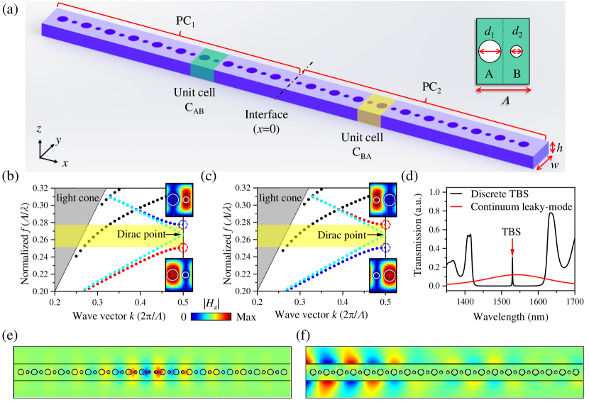
The proposed 1D-TPC embedded in a silicon bus-waveguide is first designed and simulated by using FDTD technique. The schematic image is shown in Fig. 1(a) with a waveguide width and height . The structure with periodic air-holes in a bus-waveguide is similar as that in traditional PC nanobeam cavity, which forms resonance modes in the defect of a 1D PC with the same air-hole diameter. Differently, the 1D-TPC is composed of two halves of 1D-PCs, named by PC1 and PC2. PC1 includes periodically stacked unit cells (C, highlighted in dark green), which contains two inequivalent circular air-holes. The air-holes are with diameters of and (), respectively, as shown in the upper-right inset of Fig. 1(a). PC2 is mirror symmetric with PC1, which comprises the inverted unit cells C (in yellow). C and C have the same period length .
With a specific spatial inversion symmetry along the transmission direction of the bus-waveguide embedded with the 1D-TPC, a topological phase transition arising from band crossing can be realized as an analogy to the classic Su-Schrieffer-Heeger (SSH) model Su, Schrieffer, and Heeger (1979). This is reported to relate to the distinct geometric (Zak) phase of the PC structures on both sides Xiao, Zhang, and Chan (2014); Ota et al. (2018). A guaranteed existence of the localized interface state can therefore be obtained by constructing an interface (at ) with PC1 on the left and PC2 on the right. Then, an ultra-compact 1D-TPC with the strongly localized TBS could be realized.
To confirm this, by setting nm, nm, nm, nm and nm, we obtain the calculated band structures of PC1 and PC2 in the telecom-band range, respectively. Detailed images are plotted in Figs. 1(b) and (c). The frequency and wave vector in the band structure are plotted in dimensionless units as commonly used for scalable resultsJoannopoulos et al. (2008). The lowest two bands are marked with red and blue, respectively, as they have different geometric phases Xiao, Zhang, and Chan (2014); Ota et al. (2018). The cyan bands, however, refer to the PC with air-hole diameters of such as nm. For the cells with different air-hole sizes, PC1 and PC2 share a similar band structure as a pair of inverted units. A wide photonic bandgap appears in the telecom-band between the lowest (=0.251 ) and the second lowest (=0.277 ) bands, which originates from Bragg interference of specific periodic refractive index distributions.
However, if we gradually reduce while increasing , then the photonic bandgap will gradually narrow. For the critical point when , Dirac point appears at a frequency of 0.266 , as implied by the arrows in Figs. 1(b) and (c). That is, the band goes through the process of closing, crossing, and reopening again until , which indicates a topological phase transition during the whole process Xiao, Zhang, and Chan (2014). The exchanged mode profile of the lowest two bands at the edges are given in the inset of Figs. 1(b) and (c) as well to confirm the existence of band inversion.
By further constructing PC1 and PC2 together, the TBS mode is observed from its transmission spectrum, as plotted in Fig. 1(d). Here, PC1 and PC2 are both designed with finite length of 10 unit cells. By scanning over the entire stopband, only one resonance peak is obtained as expected at the wavelength of 1529.6 nm with a factor of 1,500. To be noted here, by increasing the number of unit cells and using a finer simulation grid, a higher factor can be further obtained. This mode is located close to the center of the stopband and is far away from the band edge. It would be helpful to provide a new way with more freedom to avoid the control of mode number in a traditional multi-mode PC nanobeam cavity Xie et al. (2021). The electrical field profile of this standalone resonant mode is presented in Fig. 1(e). This TBS mode is strongly localized with a small volume of about 0.53.
To realize the topology-based Fano resonance, an extra quasi-continuum or continuum state is needed to interact with this discrete TBS Fano (1961). Fortunately, a high-order quasi-transverse electric leaky mode of the silicon bus-waveguide can be excited through a laterally tapered waveguide structure Mehta, Orcutt, and Ram (2013), which has a transmission spectrum shown in Fig. 1(d). Detailed electrical field profile of this high-order mode is presented in Fig. 1(f). The role of this leaky wave is to function as the continuum state. Thus, the resonant TBS of 1D-TPC can interfere with the excited high-order leaky mode and finally results in the asymmetric Fano lineshapes in the transmission spectrum. The whole process will be then analyzed by transfer matrix method and confirmed in our experiments.
III transfer matrix method
To facilitate the analysis using the transfer matrix method, we schematically display the transfer matrix model of the proposed 1D-TPC structure in Fig. 2(a). PC1 and PC2 discussed above constitute the 1D-TPC within the bus-waveguide. Laterally tapered waveguides are directly connected to the 1D-TPC on both sides. High-order mode (blue arrows) of the bus-waveguide is transmitted as a leaky wave through the 1D-TPC region to interfere with the inside discrete TBS mode (red arrow).
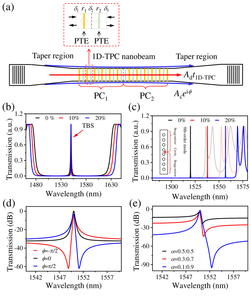
For the proposed 1D-TPC, the air-holes in a unit cell could be viewed as two partially reflecting elements (PTEs) with distinct amplitude reflection coefficient of and , as displayed in the inset of Fig. 2(a). Thus, the transmission coefficient of the 1D-TPC could be easily calculated by transfer matrix method. For example, the transfer matrix of unit cell C can be described as
| (6) |
where is the transfer matrix of the PTE for the larger and small air-holes. respectively represents the transfer matrix of the three waveguide-segments beside the two air-holes, which has phase shift of the guiding wave. Similarly, the transfer matrix of the inversion unit C can be described by
| (7) |
Therefore, the transmission of the 1D-TPC can be expressed by
| (8) |
The transfer matrices relates the incoming and outgoing wave amplitudes and at the same time. is the periods of the unit cells. Then the normalized amplitude transmission coefficient can be obtained from the relationship
| (9) |
by assuming and . For the whole system, the discrete TBS mode would interfere with the continuum leaky mode at sides of the bus-waveguide and results in the Fano resonance profile. Thus, the final transmission is
| (10) |
where is the relative phase between the two states and and are respectively amplitudes of them.
By assuming ,[m] and , for example, the transmission spectra can be obtained numerically from Eq. 10. An isolated high- resonance peak at the wavelength of 1550 nm emerges in the center of the ultra-wide stopband background with a band range over 100 nm, as displayed in Fig. 2(b). This confirms the existence of TBS discussed in Fig. 1. In addition, as the reflectivity of the PTEs increases by, such as 10% () and 20% (), the linewidth of the TBS peak narrows as well. However, the resonant wavelength remains unchanged though the reflectivity varies. This gives a special property to compare with a traditional PC nanobeam cavity based on Bragg reflection Ohta et al. (2011). As shown in Fig. 2(c), 0th-order resonance mode of the Bragg-nanobeam is similarly calculated using transfer matrix at 1520 nm with a reference air-hole reflectivity . When the reflectivity of the air-hole increases by 10% () and 20% (), the resonant wavelength shifts with the reflectivity variation. It will cause a large deviation in the expected working wavelength during device fabrication. This robust feature of 1D-TPC contributes to a tolerant way to solve the problem of wavelength shift caused mode mis-overlapping between coupled cavities. For example, it is beneficial for the Fano resonance that arises from the interference between several discrete states Zangeneh-Nejad and Fleury (2019); Wang et al. (2020).
In the proposed structure schematically shown in Fig. 2(a), we consider the interaction between the continuum high-order leaky mode and the discrete TBS with a relative amplitude ratio of, for example, . Then asymmetric Fano lineshapes can be obtained with the change of relative phase . Figure 2(d) shows the calculated Fano lineshapes via different relative phase . When , standard Lorentzian lineshape can be observed and the asymmetric factor tends to infinity. For by contrast, both constructive and destructive interferences occur. The interference between the TBS and leaky mode gives rise to the sharp asymmetric Fano lineshapes in transmission spectrum. With a doubled ER and a much higher slope rate (SR), this is beneficial for high sensitivity sensing and low power consumption optical switching.
For a fixed relative phase of , for example, the ER of the Fano lineshape can be further improved by adjusting the relative strength , as plotted in Fig. 2(e). Obviously, a decreased ratio of the continuum mode can cause a significant increase of ER while slightly sacrifice SR. However, it is not easy to change the parameters independently as the relative phase is closely related to the amplitude ratio for a multi-mode system. This may contribute to the complex kinky phase-matching relationship during the mode conversion in the taper region. It is necessary to find a balance between these two points.
IV Experiment
To verify above theoretical analyses, we fabricate several proposed 1D-TPCs with different structural parameters embedded in a bus-waveguide. The devices are fabricated on a commercial silicon-on-insulator (SOI) substrate with a 220 nm thick top silicon layer and a 2 m thick buried oxide layer. Electron beam lithography is used to define the device patterns followed by the transfer into the top silicon layer by inductively coupled plasma etching. Telecom-band grating couplers centered around 1575 nm with two-dimensional air-hole arrays are designed at both ends of the bus-waveguide Liu et al. (2010). The mode size converter is constructed with 200 m-long waveguide laterally tapered from 15 m to directly connected with a 500 nm wide bus-waveguide. Figure 3(a) displays an optical microscope image of the fabricated device. The scanning electron microscope (SEM) image of the 1D-TPC is zoomed in Fig. 3(b) with a compact footprint of 16 m 0.5 m. 20 periods of unit cells are arranged on each side of the topological interface with an adjusted period of nm. The air-hole diameters are measured of 154 nm and 94 nm, respectively.
The fabricated devices are characterized by coupling a narrowband tunable laser (TL) into the input grating coupler, and the transmission powers are monitored by an optical power meter at the other grating coupler. By sweeping the TL wavelength over a range of 1500 to 1630 nm in steps of 0.1 nm, the device transmission spectrum could be obtained. As displayed in Fig. 3(c), an isolated TBS appears at wavelength of 1574.7 nm in a stopband background with a band range over 90 nm. The factor is fitted to be 1,950 in the inset with standard Lorentzian function and this value could be much higher by further structure optimizations.
To realize the proposed asymmetric Fano resonance, an extra relative phase between the continuum leaky mode and the discrete TBS is needed, as discussed in Fig. 2(d). In our experiment, we achieve this relative phase by slightly shifting the input fiber with respect to the grating coupler Mehta, Orcutt, and Ram (2013). The output fiber is fixed considering its location would not act any effect on the propagating modes. When the fiber is aligned to the central axis of the grating coupler (shown in the upper right inset of Fig. 3(c)), the relative phase is equal to zero owing to the internal symmetry. So that the resonant transmission of the 1D-TPC dominates to support discrete TBS as shown in Fig. 3(c) with an asymmetric factor as infinity. If the input fiber has an upward or downward dislocation relative to the central axis of grating coupler, is no longer equal to zero due to the broken symmetry. A larger dislocation will result in a larger between the two states. A qualitative relationship between the phase and the dislocation can be summarized by comparing the theoretical analysis with the experimental data, which is . is the dislocation needed for a phase difference of . This relationship is reported to be closely related to the opposite parity between the fundamental (even) and high-order modes (odd) that excited in the tapered waveguide Mehta, Orcutt, and Ram (2013).
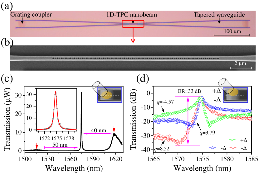
For the case that the fiber has an upward dislocation, as shown in the inset of Fig. 3(d), the relative phase is positive. Then the spectrum presents asymmetric Fano lineshape with an ER of 20.5 dB and a SR of 10.78 dB/nm, as shown by the green line in Fig. 3(d). The asymmetric factor is equal to -4.57 corresponding to a close to and an amplitude ratio around 0.52:0.48 between the modes according to Eq. 10. However, for the case with a downward dislocated input fiber, the lineshape will become an inverted Fano lineshape (as presented in the red lines of Fig. 3(d)) with an negative relative phase around , which agrees with the theoretical analysis in Fig. 2(d). Parameters of the lines are calculated to have a similar ER of 21 dB and an SR of 10.07 dB/nm. A much higher ER is realized as discussed theoretically in Fig. 2(e) by carefully tuning the fiber dislocation to decrease the proportion of the continuum leaky mode to about 0.3. With a relevant of , the measured ER is about 33 dB at the cost of a slight decrease in SR. This value is expected to be much higher than 33 dB theoretically (45 dB), which is limited by the detection limit of the employed photodiode. Note, though the relative phase is controlled by the fiber position here, optomechanics or integrated photonic MEMS are expected to realize a more precise and flexible dislocation in future device for more compact devices. Besides, compact mode multiplexer can be integrated as well to realize a similar operationZhang et al. (2018).
V Conclusion
In conclusion, we have demonstrated an ultra-compact 1D-TPC structure to generate Fano resonance lineshapes by interfering a discrete TBS with a continuum high-order leaky mode. With the topological feature of the demonstrated 1D-TPC, the TBS represents as an isolated resonance peak in the center of a flat background over 90 nm, which is beneficial for the single mode operation of the on-chip device applications. By exciting the continuum high-order leaky mode of the 1D-TPC, the Fano resonance lineshapes are obtained. From the fabricated device, lineshapes with an ER over 33 dB and a SR around 10 dB/nm are obtained, which could also be tuned by controlling the coupling condition of the input light. Our results might open a new avenue to develop high-performance on-chip optical switch, sensing, and laser based on Fano resonance lineshapes.
Fundings
The Key Research and Development Program (2017YFA0303800), National Natural Science Foundation (91950119, 11634010, 61775183, 61905196), the Key Research and Development Program in Shaanxi Province of China (2020JZ-10), the Fundamental Research Funds for the Central Universities (310201911cx032, 3102019JC008).
Acknowledgment
The authors would thank the Analytical & Testing Center of NPU for the assistances of device fabrication.
References
- Fano [1961] U. Fano, “Effects of configuration interaction on intensities and phase shifts,” Physical Review 124, 1866 (1961).
- Yu et al. [2016] Y. Yu, W. Xue, H. Hu, L. K. Oxenløwe, K. Yvind, and J. Mork, “All-optical switching improvement using photonic-crystal fano structures,” IEEE Photonics Journal 8, 1–8 (2016).
- Limonov et al. [2017] M. F. Limonov, M. V. Rybin, A. N. Poddubny, and Y. S. Kivshar, “Fano resonances in photonics,” Nature Photonics 11, 543 (2017).
- Yu et al. [2017] Y. Yu, W. Xue, E. Semenova, K. Yvind, and J. Mork, “Demonstration of a self-pulsing photonic crystal fano laser,” Nature Photonics 11, 81–84 (2017).
- Yi, Citrin, and Zhou [2010] H. Yi, D. Citrin, and Z. Zhou, “Highly sensitive silicon microring sensor with sharp asymmetrical resonance,” Optics Express 18, 2967–2972 (2010).
- Tu et al. [2017] Z. Tu, D. Gao, M. Zhang, and D. Zhang, “High-sensitivity complex refractive index sensing based on fano resonance in the subwavelength grating waveguide micro-ring resonator,” Optics Express 25, 20911–20922 (2017).
- Zhang et al. [2020a] C. Zhang, G. Kang, Y. Xiong, T. Xu, L. Gu, X. Gan, Y. Pan, and J. Qu, “Photonic thermometer with a sub-millikelvin resolution and broad temperature range by waveguide-microring fano resonance,” Optics Express 28, 12599–12608 (2020a).
- Nozaki et al. [2013] K. Nozaki, A. Shinya, S. Matsuo, T. Sato, E. Kuramochi, and M. Notomi, “Ultralow-energy and high-contrast all-optical switch involving fano resonance based on coupled photonic crystal nanocavities,” Optics Express 21, 11877–11888 (2013).
- Yu et al. [2014] Y. Yu, M. Heuck, H. Hu, W. Xue, C. Peucheret, Y. Chen, L. K. Oxenløwe, K. Yvind, and J. Mørk, “Fano resonance control in a photonic crystal structure and its application to ultrafast switching,” Applied Physics Letters 105, 061117 (2014).
- Heuck et al. [2013] M. Heuck, P. T. Kristensen, Y. Elesin, and J. Mørk, “Improved switching using fano resonances in photonic crystal structures,” Optics Letters 38, 2466–2468 (2013).
- Zhang, Li, and Yao [2016] W. Zhang, W. Li, and J. Yao, “Optically tunable fano resonance in a grating-based fabry–perot cavity-coupled microring resonator on a silicon chip,” Optics Letters 41, 2474–2477 (2016).
- Qiu et al. [2012] C. Qiu, P. Yu, T. Hu, F. Wang, X. Jiang, and J. Yang, “Asymmetric fano resonance in eye-like microring system,” Applied Physics Letters 101, 021110 (2012).
- Gu et al. [2019] L. Gu, H. Fang, J. Li, L. Fang, S. J. Chua, J. Zhao, and X. Gan, “A compact structure for realizing lorentzian, fano, and electromagnetically induced transparency resonance lineshapes in a microring resonator,” Nanophotonics 8, 841–848 (2019).
- Gu et al. [2020] L. Gu, L. Fang, H. Fang, J. Li, J. Zheng, J. Zhao, Q. Zhao, and X. Gan, “Fano resonance lineshapes in a waveguide-microring structure enabled by an air-hole,” APL Photonics 5, 016108 (2020).
- Fang et al. [2020] L. Fang, L. Gu, J. Zheng, Q. Zhao, X. Gan, and J. Zhao, “Controlling resonance lineshapes of a side-coupled waveguide-microring resonator,” Journal of Lightwave Technology 38, 4429–4434 (2020).
- Li et al. [2012] B.-B. Li, Y.-F. Xiao, C.-L. Zou, X.-F. Jiang, Y.-C. Liu, F.-W. Sun, Y. Li, and Q. Gong, “Experimental controlling of fano resonance in indirectly coupled whispering-gallery microresonators,” Applied Physics Letters 100, 021108 (2012).
- Raghu and Haldane [2008] S. Raghu and F. D. M. Haldane, “Analogs of quantum-hall-effect edge states in photonic crystals,” Physical Review A 78, 033834 (2008).
- Chen et al. [2017] X.-D. Chen, F.-L. Zhao, M. Chen, and J.-W. Dong, “Valley-contrasting physics in all-dielectric photonic crystals: Orbital angular momentum and topological propagation,” Physical Review B 96, 020202 (2017).
- Khanikaev and Shvets [2017] A. B. Khanikaev and G. Shvets, “Two-dimensional topological photonics,” Nature Photonics 11, 763–773 (2017).
- Ota et al. [2018] Y. Ota, R. Katsumi, K. Watanabe, S. Iwamoto, and Y. Arakawa, “Topological photonic crystal nanocavity laser,” Communications Physics 1, 1–8 (2018).
- Zhang et al. [2020b] W. Zhang, X. Xie, H. Hao, J. Dang, S. Xiao, S. Shi, H. Ni, Z. Niu, C. Wang, K. Jin, et al., “Low-threshold topological nanolasers based on the second-order corner state,” Light: Science & Applications 9, 1–6 (2020b).
- Shao et al. [2020] Z.-K. Shao, H.-Z. Chen, S. Wang, X.-R. Mao, Z.-Q. Yang, S.-L. Wang, X.-X. Wang, X. Hu, and R.-M. Ma, “A high-performance topological bulk laser based on band-inversion-induced reflection,” Nature Nanotechnology 15, 67–72 (2020).
- Han et al. [2019] C. Han, M. Lee, S. Callard, C. Seassal, and H. Jeon, “Lasing at topological edge states in a photonic crystal l3 nanocavity dimer array,” Light: Science & Applications 8, 1–10 (2019).
- Li et al. [2018] F.-F. Li, H.-X. Wang, Z. Xiong, Q. Lou, P. Chen, R.-X. Wu, Y. Poo, J.-H. Jiang, and S. John, “Topological light-trapping on a dislocation,” Nature Communications 9, 1–8 (2018).
- Shalaev et al. [2019] M. I. Shalaev, W. Walasik, A. Tsukernik, Y. Xu, and N. M. Litchinitser, “Robust topologically protected transport in photonic crystals at telecommunication wavelengths,” Nature Nanotechnology 14, 31–34 (2019).
- He et al. [2019] X.-T. He, E.-T. Liang, J.-J. Yuan, H.-Y. Qiu, X.-D. Chen, F.-L. Zhao, and J.-W. Dong, “A silicon-on-insulator slab for topological valley transport,” Nature Communications 10, 1–9 (2019).
- Gao et al. [2018] W. Gao, X. Hu, C. Li, J. Yang, Z. Chai, J. Xie, and Q. Gong, “Fano-resonance in one-dimensional topological photonic crystal heterostructure,” Optics Express 26, 8634–8644 (2018).
- Zangeneh-Nejad and Fleury [2019] F. Zangeneh-Nejad and R. Fleury, “Topological fano resonances,” Physical Review Letters 122, 014301 (2019).
- Wang et al. [2020] W. Wang, Y. Jin, W. Wang, B. Bonello, B. Djafari-Rouhani, and R. Fleury, “Robust fano resonance in a topological mechanical beam,” Physical Review B 101, 024101 (2020).
- Ji, Zhang, and Yao [2021] C.-Y. Ji, Y. Zhang, and Y. Yao, “Topologically protected fano resonance in photonic valley hall insulators,” Physical Review A 103, 023512 (2021).
- Su, Schrieffer, and Heeger [1979] W. Su, J. Schrieffer, and A. J. Heeger, “Solitons in polyacetylene,” Physical Review Letters 42, 1698 (1979).
- Xiao, Zhang, and Chan [2014] M. Xiao, Z. Zhang, and C. T. Chan, “Surface impedance and bulk band geometric phases in one-dimensional systems,” Physical Review X 4, 021017 (2014).
- Joannopoulos et al. [2008] J. D. Joannopoulos, S. G. Johnson, J. N. Winn, and R. D. Meade, “Molding the flow of light,” Princeton Univ. Press, Princeton, NJ [ua] (2008).
- Xie et al. [2021] W. Xie, P. Verheyen, M. Pantouvaki, J. Van Campenhout, and D. Van Thourhout, “Efficient resonance management in ultrahigh-q 1d photonic crystal nanocavities fabricated on 300 mm soi cmos platform,” Laser & Photonics Reviews 15, 2000317 (2021).
- Mehta, Orcutt, and Ram [2013] K. K. Mehta, J. S. Orcutt, and R. J. Ram, “Fano line shapes in transmission spectra of silicon photonic crystal resonators,” Applied Physics Letters 102, 081109 (2013).
- Ohta et al. [2011] R. Ohta, Y. Ota, M. Nomura, N. Kumagai, S. Ishida, S. Iwamoto, and Y. Arakawa, “Strong coupling between a photonic crystal nanobeam cavity and a single quantum dot,” Applied Physics Letters 98, 173104 (2011).
- Liu et al. [2010] L. Liu, M. Pu, K. Yvind, and J. M. Hvam, “High-efficiency, large-bandwidth silicon-on-insulator grating coupler based on a fully-etched photonic crystal structure,” Applied Physics Letters 96, 051126 (2010).
- Zhang et al. [2018] J. Zhang, X. Leroux, E. Durán-Valdeiglesias, C. Alonso-Ramos, D. Marris-Morini, L. Vivien, S. He, and E. Cassan, “Generating fano resonances in a single-waveguide silicon nanobeam cavity for efficient electro-optical modulation,” ACS Photonics 5, 4229–4237 (2018).