Sensing dot with high output swing for scalable baseband readout of spin qubits
Abstract
A crucial requirement for quantum computing, in particular for scalable quantum computing and error correction, is a fast and high-fidelity qubit readout. For semiconductor based qubits, one limiting factor for local low-power signal amplification, is the output swing of the charge sensor. We demonstrate GaAs and Si/SiGe asymmetric sensing dots (ASDs) specifically designed to provide a significantly improved response compared to conventional charge sensing dots. Our ASD design features a strongly decoupled drain reservoir from the sensor dot, which mitigates negative feedback effects found in conventional sensors. This results in a boosted output swing of , which exceeds the response in the conventional regime of our device by more than ten times. The enhanced output signal paves the way for employing very low-power readout amplifiers in close proximity to the qubit.
Introduction
Spin qubits based on gate-defined quantum dots (QDs) use proximal charge sensors 1; 2 and, more recently, dispersive gate sensing techniques 3; 4; 5 for readout of the quantum state after spin-to-charge conversion 6; 7. Proximal charge sensors can be quantum point contacts or sensing dots (SDs), with the latter being the most sensitive sensor for spin qubit readout. The focus of new readout circuits is shifting towards scalability, as high-fidelity, scalable readout is a key requirement for quantum computers with more than just a few qubits.
The state-of-the-art readout technique is based on RF reflectometry 8, which satisfies the requirement of high fidelity and provides the largest bandwidths to date. Depending on the qubit scaling strategy, RF reflectometry may be the method of choice, as there are solutions to miniaturize at least parts of the necessary RF components 9 or use multiplexing techniques 10; 11; 12, for example, in the context of a crossbar qubit architecture 13. However, the overall readout periphery is complex, and necessary RF components are currently on the centimeter scale.
Baseband readout, using optimized transistor circuits in close proximity to the qubit, may prove decisive for scaling strategies where readout and some control functionality are integrated near each qubit, as for example proposed for the spider web array 14. Single-shot readout using a HEMT amplifier has been demonstrated 15, and the performance was improved for amplifiers adjacent to the sample 16; 17; 18. Increasing the SD output signal would allow an even lower total power consumption, thus more simultaneous qubit readouts or a higher readout fidelity using the baseband readout approach, since the power requirement is determined by amplifier gain and sensitivity. In conventional sensing dots, however, the output swing is limited by negative feedback, due to a large drain capacitance, analogous to the Miller effect in classical electronics 19.
In this study, we introduce a proximal charge sensor designed specifically to create an asymmetric sensing dot (ASD) by utilizing additional electrodes to sculpt the electrostatic potential of an SD. Our main goal is to investigate the performance of this novel gate concept for ASD realization. We perform voltage bias transport measurements, observing a significant reduction in dot and drain capacitive coupling in Coulomb diamonds. We find qualitatively similar results in remote doped GaAs/(Al,Ga)As and undoped Si/SiGe devices, supporting the universality of the concept. Additionally, we use the ASD for charge sensing in a nearby qubit-like double quantum dot (DQD) tuned into a multi-electron regime.
By focusing on the realization and investigation of the ASD gate concept, we aim to establish a foundation for further research into the potential of this sensor design for scalable baseband readout quantum circuits. The ASD allows for a trade-off between the expanded footprint of the sensor gate layout, owing to additional gate electrodes, and its boosted signal output. Recent investigations into the qubit shuttling architecture have eased the requirements on the former aspect 20, as demonstrated by Seidler et al. 21.
ASD Concept
Figure 1(a) illustrates the electric potential of a biased SD. The ladder of QD energy levels can be shifted by the gate voltage , while a bias is applied to the drain D. Measuring the transport current through the device while driving these voltages produces a characteristic diamond-shaped pattern due to Coulomb blockade effects. A section of these diamonds is depicted in panel figure 1(b), where current flows only in the gray regions. According to a constant interaction model 22, the positive and negative slopes of the Coulomb diamonds are and , where is the dot’s total capacitance to ground, and and are the capacitance to the swept gate electrode and drain reservoir, respectively. In the SD, the drain D is separated from the dot by a sharp tunneling barrier, similar to the source S, as depicted by the top sketch in figure 1(b).
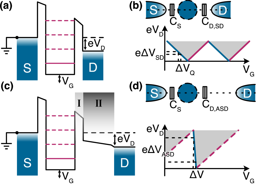
The ASD concept presented in this study is focused on modifying the drain barrier such that the tunneling rate remains comparable to the conventional SD, while significantly reducing the drain capacitance to increase the maximum output voltage. To achieve this, the barrier is subdivided into a compound barrier with a sharp tunnel barrier region I and an additional slowly decreasing barrier region II termed slide. Region II physically separates the drain reservoir further from the dot, resulting in , while region I controls the tunneling at the working point. The top sketch figure 1(d) shows the new SD configuration, where the asymmetric arrangement of source and drain is visible, hence the name ASD.
Figure 1(c) displays the electric potential of a biased ASD. An equivalent shift on the axis now results in a greatly enhanced shift for the ASD compared to . Therefore, an essential figure of merit for the ASD is the magnitude of the blue slope in figure 1(d), where larger values indicate a higher output voltage swing of the sensor when configured for charge sensing.
Experimental Results
Figure 2(a) displays a false-colored scanning electron microscope (SEM) image of a double quantum dot (DQD) integrated with an ASD on the left. The ASD is incorporated into our GaAs qubit design, utilizing a doped MBE-grown GaAs/(Al,Ga)As heterostructure, which features a 2DEG 90 nm beneath the interface (see supplemental material for heterostructure details) 23; 24.
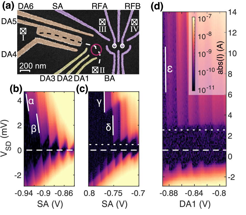
The yellow-colored gates DA(1-3) define an SD, while the orange-colored gates DA(4-6) control the dot-drain transition. The purple-colored gates are used to define and manipulate the nearby DQD. The source reservoir (labeled ⌧ II) has a common distance from the SD (red circle) used for conventional SDs, while the drain reservoir (⌧ I) is asymmetrically formed. A dashed line illustrates a possible electron path connecting the sensor’s source and drain. Supported by numerical electrostatic simulations, we developed device designs optimizing the drain barrier potential region for a slow and monotonically declining transition to the drain reservoir, effectively creating a micron-scale electron slide with sharp tunnel barriers defining the SD 25. Transport at the optimal working point is still possible, while the capacitive coupling of dot and drain is significantly reduced.
To experimentally validate the ASD concept, we compare Coulomb diamonds of the sensor tuned for conventional operation with nearly symmetric source and drain barriers (gates DA(4-6) set to ) in figure 2(b), to a tuned up ASD in figure 2(c). The sensor is operated in the multi-electron Coulomb blockade regime with a voltage bias applied to ohmic contact ⌧ II (drain), while current is measured with a transimpedance amplifier at ⌧ I (source).
Typical values of do not exceed a few hundred V for conventional SD operation. In the following, values of can easily exceed several mV, since the compound drain barrier of the ASD becomes only transparent at higher bias voltages. Figure 2(b) shows typical Coulomb diamonds, when operating the device in a conventional way without using the additional gate electrodes, that are symmetric around zero bias. Gate SA not only shifts the dot minimum, but also modifies the tunneling rates of the dot barriers, thus the diamond features become smeared out for higher tunneling rates at more positive voltages. At more negative voltages transport is blocked close to zero bias, as the barriers become opaque. The slope of the diamond can be evaluated at different current levels. Here we choose , which is a compromise between low current operation and a sufficient signal-to-noise ratio. In figure 2(b) we fit a line at the contour and find a maximum slope of for the SD. Note, that for a conventional SD the slope remains nearly constant even at higher bias values.
Figure 2(c) shows equivalent measurements with the sensor tuned to the ASD regime. The Coulomb diamonds change distinctively from the conventional case and the positive and negative bias configurations are not symmetric anymore. A bias dependence of the Coulomb lines is observed for slopes and of the ASD, compared to and for the SD. At higher bias, a maximal slope of at the contour is observed111On a side note: Since , the ASD has voltage gain and can be used as an ultra low-power, low stray capacitance voltage amplifier in principle, with the limitation of a narrow dynamics range.. The steepening of Coulomb diamonds indicates the desired reduction of by a factor of , compared to the maximal slope in figure 2(b). Additionally, we observe a bias window in figure 2(c), where transport is blocked (, where ), in between the dashed and dotted white lines. We find in figure 2(d) that when a nearby DQD is also tuned up, can be of the order of several mV, which results in low visibility of the typical Coulomb blockade features near zero bias. Further details of ASD tuning and characteristic features are discussed in the supplemental material.
To test the adaptability of our ASD concept, we also realized a device in a MBE-grown Si/SiGe heterostructure, featuring a nm thick Si QW separated from the interface by a nm thick spacer 27 (see supplemental material for heterostructure details). Transferring the ASD from a remote-doped GaAs to an undoped Si/SiGe heterostructure requires a full redesign of the gate pattern: First, Si/SiGe requires an accumulation gate also above the slide region and second the gate pattern has to be shrunken down to compensate for the three times larger effective electron mass. Therefore, we implemented a new simulation-guided design to host the ASD and a nearby DQD.
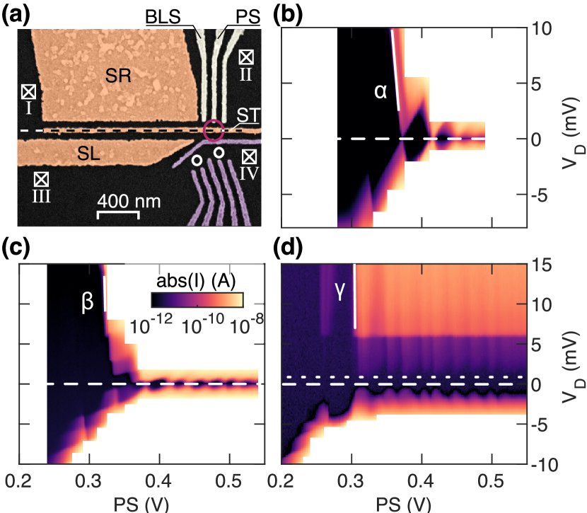
A false-colored SEM image of this gate layout is shown in figure 3(a). The sensor dot is formed by the light yellow colored gates, from which gate PS serves as the plunger gate for the sensor quantum dot levels. Gates SL, SR and ST (colored orange) form the potential slide (region II in figure 1(c)) and the purple colored gates may be used to tune two tunnel-coupled QDs in the vicinity of the sensor dot. Current through the sensor is defined by ohmic contacts ⌧ I and ⌧ II, while contacts ⌧ III and ⌧ IV serve as electron reservoirs for the DQD. Tuning the electrostatic potential to form a sensor QD below gate PS, we record a series of Coulomb blockade measurements to test the tunability of the slide potential region II. Starting from a conventional symmetric configuration in figure 3(b), the slide is then activated by only reducing the voltage on gate SR, while simultaneously increasing the voltage on gate BLS to retain the same tunnel rate (keep region I in figure 1(b) constant) for transport through the sensor. In figure 3(b)-(d), we decreased the voltage on gate SR from 0.34 V to 0.24 V and 0.215 V, respectively. Similar to the observation in GaAs, for the most negative SR configuration a blockade region with a threshold voltage of emerges222Even lower voltages on SR led to yet higher ..
The series in figure 3(b)-(d) clearly shows that the negative Coulomb diamond edges become steeper, the smaller the voltage applied to the gate SR. For all three diamonds shown here, we determined these negative Coulomb diamond slopes, by fitting the contour, which represents the best compromise between a low-current operation of the device and a sufficient signal-to-noise ratio. The slopes in figure 3(b)-(d) represent the steepest slopes which we found for each configuration333Interpolation of the data sets along the plunger gate (PS) direction was used to compensate for the lower measurement resolution on this gate.. Starting from for the most symmetric configuration, we reach for the intermediate configuration and finally for the most asymmetric configuration, corresponding to a twelve-fold reduction of .
Hence, we have shown that the ASD concept is equally efficient across material platforms. Integrating ASDs into a DQD environment, we have demonstrated a controllable reduction of both in Si/SiGe and GaAs while being able to maintain a tunneling rate useful for operation of the sensor quantum dot. In the proof-of-principle experiments discussed in figures 2 and 3, we reached a maximal reduction of by a factor of 13 in GaAs and a factor of 12 in Si/SiGe, implying an increase by the same factor of the voltage swings produced by these ASDs, compared to conventional SD operation.
ASD charge sensing
We demonstrate charge sensing operation with the ASD by defining a DQD in the center of the GaAs device, using the purple colored gates shown in figure 2. For charge sensing, it is crucial to reconfigure the ASD for current bias to take advantage of the high output voltage swing. In this case, a constant current source supplies 500 pA through the drain, while the source is grounded. We tune the ASD to a sensitive position and record a charge stability diagram of the DQD using gates RFA and RFB, as shown in figure 4(a) (see supplemental material for tuning details).
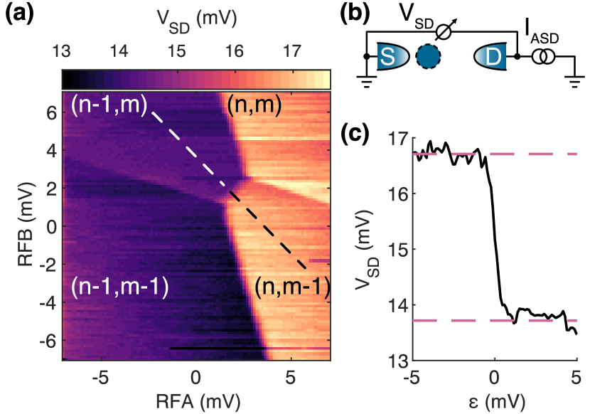
The voltage drop across the ASD is monitored with a voltmeter, as shown in figure 4(b). Figure 4(c) displays the voltage swing across the inter-dot transition of the DQD (dashed line in figure 4(a)), corresponding to a qubit state change when the DQD is used as an ST-qubit. We observe a voltage swing of 3 mV. The voltage swing is expected to be an order of magnitude larger than that of a conventional SD in this configuration due to the one order of magnitude difference in slopes and seen in figure 2. These slopes provide a measure of sensor sensitivity, as discussed in figure 1(c)-(d).
Discussion
In conclusion, we have presented a novel type of proximal charge sensor specifically designed for the formation of ASDs as the main goal of this study. Our findings showcase the successful implementation of an ASD gate concept that is adaptable across various material systems. This is evidenced by the drain capacitance reduction by factors of 12 and 13 respectively in both undoped Si/SiGe and doped GaAs devices when compared to conventional SD operation. It is worth noting that the GaAs device serves as a demonstrator, and we anticipate that the ASD is more likely to be relevant for Si-based spin qubit architectures, where nuclear fluctuations play a less significant role and CMOS processing techniques can be employed. The next experimental step involves integrating the ASD with published work on transistors 15; 16; 17 and examining the extent to which the ASD affects the host qubit, considering the higher energy electrons generated during sensor operation compared to conventional SDs 30; 31.
Data availability
The data sets generated and/or analyzed during this study are available from the corresponding author upon reasonable request.
Acknowledgements
This work was funded by ARO under the contract NO W911NF-17-1-0349 titled ”A scalable and high performance approach to readout of silicon qubits” and by the German Research Foundation (DFG) within the project BO 3140/4-1. The device fabrication has been done at HNF - Helmholtz Nano Facility, Research Center Juelich GmbH 32.
Competing interests
The authors declare no competing interests.
Author contributions
The study was conceived by H.B. L.R.S. and D.B. The GaAs heterostructures were prepared by J.R. A.L. and A.W. and sample fabrication performed by M.K. E.K. conducted the experiments data analysis and numerical simulations on the GaAs samples, advised by H.B. The Si/SiGe heterostructures were prepared by D.B. Numerical simulations, the device design and the sample fabrication for Si/SiGe was performed by I.S. M.N. and L.R.S. A.S. L.D. and D.B. conducted the experiments and the data analysis on the Si/SiGe samples. All authors discussed the results. E.K. A.S. L.D. D.B. L.R.S. and H.B. wrote the manuscript.
References
- Field et al. (1993) M. Field, C. G. Smith, M. Pepper, D. A. Ritchie, J. E. Frost, G. A. Jones, and D. G. Hasko, Phys. Rev. Lett. 70, 1311 (1993).
- Schoelkopf et al. (1998) R. J. Schoelkopf, P. Wahlgren, A. A. Kozhevnikov, P. Delsing, and D. E. Prober, Science 280, 1238 (1998).
- Colless et al. (2013) J. I. Colless, A. C. Mahoney, J. M. Hornibrook, A. C. Doherty, H. Lu, A. C. Gossard, and D. J. Reilly, Phys. Rev. Lett. 110, 1 (2013).
- West et al. (2019) A. West, B. Hensen, A. Jouan, T. Tanttu, C.-H. Yang, A. Rossi, M. F. Gonzalez-Zalba, F. Hudson, A. Morello, D. J. Reilly, and A. S. Dzurak, Nat. Nanotechnol. 14, 437 (2019).
- Zheng et al. (2019) G. Zheng, N. Samkharadze, M. L. Noordam, N. Kalhor, D. Brousse, A. Sammak, G. Scappucci, and L. M. K. Vandersypen, Nat. Nanotechnol. 14, 742 (2019).
- Willems van Beveren et al. (2003) L. H. Willems van Beveren, S. Tarucha, J. M. Elzerman, J. S. Greidanus, R. Hanson, S. De Franceschi, L. M. Vandersypen, L. P. Kouwenhoven, S. De Franceschi, L. M. Vandersypen, S. De Franceschi, and L. M. Vandersypen, Phys. Rev. B 67, 161308 (2003).
- Johnson et al. (2005) A. C. Johnson, J. R. Petta, C. M. Marcus, M. P. Hanson, and A. C. Gossard, Phys. Rev. B 72, 1 (2005).
- Reilly et al. (2007) D. J. Reilly, C. M. Marcus, M. P. Hanson, and A. C. Gossard, Appl. Phys. Lett. 91, 162101 (2007).
- Mahoney et al. (2017) A. C. Mahoney, J. I. Colless, S. J. Pauka, J. M. Hornibrook, J. D. Watson, G. C. Gardner, M. J. Manfra, A. C. Doherty, and D. J. Reilly, Phys. Rev. X 7, 011007 (2017).
- Hornibrook et al. (2014) J. M. Hornibrook, J. I. Colless, A. C. Mahoney, X. G. Croot, S. Blanvillain, H. Lu, A. C. Gossard, and D. J. Reilly, Appl. Phys. Lett. 104, 103108 (2014).
- Hornibrook et al. (2015) J. M. Hornibrook, J. I. Colless, I. D. Conway Lamb, S. J. Pauka, H. Lu, A. C. Gossard, J. D. Watson, G. C. Gardner, S. Fallahi, M. J. Manfra, and D. J. Reilly, Phys. Rev. Appl. 3, 1 (2015).
- Schaal et al. (2018) S. Schaal, S. Barraud, J. J. Morton, and M. F. Gonzalez-Zalba, Phys. Rev. Appl. 9, 54016 (2018).
- Li et al. (2018) R. Li, L. Petit, D. P. Franke, J. P. Dehollain, J. Helsen, M. Steudtner, N. K. Thomas, Z. R. Yoscovits, K. J. Singh, S. Wehner, L. M. Vandersypen, J. S. Clarke, and M. Veldhorst, Sci. Adv. 4, 1 (2018).
- Boter et al. (2022) J. M. Boter, J. P. Dehollain, J. P. Van Dijk, Y. Xu, T. Hensgens, R. Versluis, H. W. Naus, J. S. Clarke, M. Veldhorst, F. Sebastiano, and L. M. Vandersypen, Phys. Rev. Appl. 18, 1 (2022).
- Vink et al. (2007) I. T. Vink, T. Nooitgedagt, R. N. Schouten, L. M. K. Vandersypen, and W. Wegscheider, Appl. Phys. Lett. 91, 23 (2007).
- Tracy et al. (2016) L. A. Tracy, D. R. Luhman, S. M. Carr, N. C. Bishop, G. A. Ten Eyck, T. Pluym, J. R. Wendt, M. P. Lilly, and M. S. Carroll, Appl. Phys. Lett. 108, 63101 (2016).
- Curry et al. (2019) M. J. Curry, M. Rudolph, T. D. England, A. M. Mounce, R. M. Jock, C. Bureau-Oxton, P. Harvey-Collard, P. A. Sharma, J. M. Anderson, D. M. Campbell, J. R. Wendt, D. R. Ward, S. M. Carr, M. P. Lilly, and M. S. Carroll, Sci. Rep. 9, 1 (2019).
- Mills et al. (2022) A. R. Mills, C. R. Guinn, M. J. Gullans, A. J. Sigillito, M. M. Feldman, E. Nielsen, and J. R. Petta, Sci. Adv. 8, 1 (2022).
- Horowitz and Hill (2015) P. Horowitz and W. Hill, The Art of Electronics, 3rd ed. (Cambridge University Press, New York, NY, USA, 2015).
- Langrock et al. (2023) V. Langrock, J. A. Krzywda, N. Focke, I. Seidler, L. R. Schreiber, and L. Cywiń, PRX Quantum 4, 20305 (2023).
- Seidler et al. (2022) I. Seidler, T. Struck, R. Xue, N. Focke, S. Trellenkamp, H. Bluhm, and L. R. Schreiber, npj Quantum Inf. 8, 100 (2022).
- Hanson et al. (2007) R. Hanson, J. R. Petta, S. Tarucha, and L. M. K. Vandersypen, Rev. Mod. Phys. 79, 1217 (2007).
- MacLeod et al. (2015) S. J. MacLeod, A. M. See, A. R. Hamilton, I. Farrer, D. A. Ritchie, J. Ritzmann, A. Ludwig, and A. D. Wieck, Appl. Phys. Lett. 106, 012105 (2015).
- Cerfontaine et al. (2020) P. Cerfontaine, T. Botzem, J. Ritzmann, S. S. Humpohl, A. Ludwig, D. Schuh, D. Bougeard, A. D. Wieck, and H. Bluhm, Nat. Commun. 11, 5 (2020).
- Kammerloher (2022) E. Kammerloher, Improving the output signal of charge readout for quantum computing in electrostatically defined quantum dots with a new sensing dot concept, Dissertation, RWTH Aachen University, Aachen (2022).
- Note (1) On a side note: Since , the ASD has voltage gain and can be used as an ultra low-power, low stray capacitance voltage amplifier in principle, with the limitation of a narrow dynamics range.
- Wild et al. (2012) A. Wild, J. Kierig, J. Sailer, J. W. Ager, E. E. Haller, G. Abstreiter, S. Ludwig, and D. Bougeard, Appl. Phys. Lett. 100, 1 (2012).
- Note (2) Even lower voltages on SR led to yet higher .
- Note (3) Interpolation of the data sets along the plunger gate (PS) direction was used to compensate for the lower measurement resolution on this gate.
- Granger et al. (2012) G. Granger, D. Taubert, C. E. Young, L. Gaudreau, A. Kam, S. A. Studenikin, P. Zawadzki, D. Harbusch, D. Schuh, W. Wegscheider, Z. R. Wasilewski, A. A. Clerk, S. Ludwig, and A. S. Sachrajda, Nat. Phys. 8, 522 (2012).
- Harbusch et al. (2010) D. Harbusch, D. Taubert, H. P. Tranitz, W. Wegscheider, and S. Ludwig, Phys. Rev. Lett. 104, 196801 (2010).
- Albrecht et al. (2017) W. Albrecht, J. Moers, and B. Hermanns, J. Large-Scale Res. Facil. 3, A112 (2017).