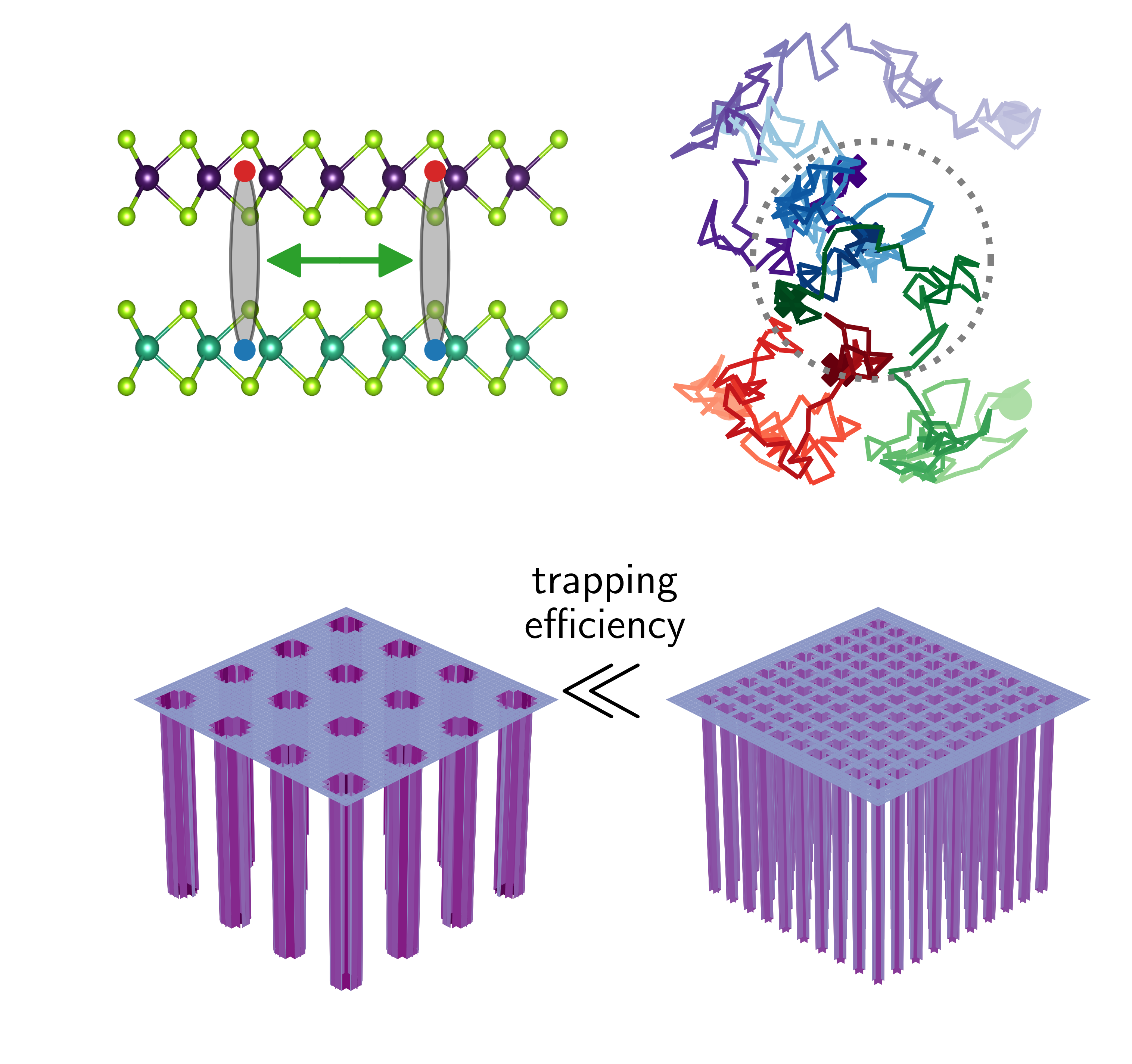
Trapping Interlayer Excitons in van der Waals Heterostructures by Potential Arrays
Abstract
Transition metal dichalcogenide heterostructures can host interlayer excitons (IXs), which consist of electrons and holes spatially separated in different layers. IXs possess permanent dipoles and have proven to offer a wealth of novel physics. We develop a discrete, random-walk model which includes annihilation and repulsion interactions among IXs. Using this model, we simulate the trapping of IXs in traps of different depths, densities, and shapes. Our results show that dipole-dipole interactions play an important role in regulating IX trapping. The effects of dipole interactions can be mitigated with small, deep traps which are realizable with atmoic defects and moiré potentials.
I Introduction
An interlayer exciton (IX) is composed of an electron and hole that are spatially separated in different layers but bound by Coulomb interactions. Due to the spatial separation of the constituent electrons and holes, IXs can have lifetimes that are orders of magnitude longer than those of intralayer excitons.[1] Furthermore, IXs possess permanent, out-of-plane electric dipole moments, rendering their binding energies effectively tunable using external electric fields.[2, 3] These characteristics may allow IXs to be cooled below the temperature of quantum degeneracy, leading to the realization of quantum Bose gases.[4, 5] Their widely tunable excitonic response is also promising for efficient light emitting and modulation applications.[6, 7]
While indirect excitons in conventional III-V semiconductor heterostructures have been extensively studied,[8, 9] those in two-dimensional transition metal dichalcogenide (TMD) heterostructures provide alternative opportunities for exploring excitonic quantum gases and devices at high temperatures[10] due to their considerably larger binding energies.[11, 12] The spin-valley degree of freedom offered by IXs in TMDs may also enable unconventional strategies for data processing and transmission.[13]
Exploration of IXs in TMD heterostructures for these applications almost exclusively rely on their trapping and localization. In order to obtain a cold and dense exciton gas for their spontaneous condensation, a potential trap is often required to accumulate the indirect excitons towards the bottom of the trap potential.[14, 15] The transport of IXs can be modulated by their localization-delocalization transitions across lattice potentials.[16, 17] Moreover, the strong repulsive dipole-dipole interactions among IXs can be engineered by confining them in potential traps created by strains, disorders or moiré potentials,[18, 19, 20] which may provide rich opportunities for the study of quantum optical nonlinearities and creation of quantum photon sources.[21, 22, 23]
While great strides have been made in trapping IXs in TMDs using strains and moiré potentials,[18, 20, 24, 25] the influence of the potential trap nature, such as the trap geometries and densities, on the related photodynamics of the IXs including their trapping and localization remain largely unexplored. Specifically, upon excitation of TMD heterostructures, IXs can be formed over picosecond timescales.[26, 27] The longer lifetimes of the IXs compared to those of the intralayer excitons indicate the potentially larger diffusion lengths of the IXs and their higher probabilities to encounter potential traps before recombination occurs.[28] The competition between the trapping and recombination of the IXs should be heavily influenced by the density and arrangement of the potential traps. Additionally, IXs may undergo trapping-detrapping dynamics depending on the experienced thermal fluctuations and dipole-dipole interactions, which are closely related to the system temperature and trap dimensions.[18, 29] These factors, combined with the intrinsic electronic structures of the TMD monolayers manifested as bright and dark excitonic states,[30, 31] constitute multiple degrees of freedom that are important to control when creating TMD devices with optimal IX trapping efficiencies.
Here, we systematically investigate the trapping and localization of IXs based on a discrete-time random walk model. By including realistic inter-exciton processes like exciton-exciton annihilation and dipole-dipole repulsion, we investigate the effects of trap dimensions and densities on IX dynamics. We show the trade-off between trap parameters like depth, radius, and density compared to externally controlled parameters like temperature and initial exciton density in achieving efficient IX trapping. We find that trap radius and dipole-dipole interaction among IXs play a dominant role in determining their trapping efficiencies. Our results evidence that myriad small traps at low temperature yield the highest trapping efficiency of IXs. These findings illustrate the influence of various parameters on IX dynamics, and provide heuristics for the design of TMD heterostructures with optimized IX trapping properties which are targeted for quantum nonlinearity and quantum photon source applications.
II Theoretical Model
In this work, we consider MoSe2/WSe2 heterobilayers (Figure 1a,b) as the prototypical TMD heterostructure for hosting IXs. The model and analysis presented here can be generalized to other heterobilayers. MoSe2/WSe2 heterobilayers have a type-II staggered band alignment, in which the lowest conduction band edges and highest valence band edges are associated with MoSe2 and WSe2, respectively (Figure 1a). Due to the order of spin-up and spin-down states in the two types of constituent monolayers,[31] the lowest IX state in a MoSe2/WSe2 heterobilayer is optically active.
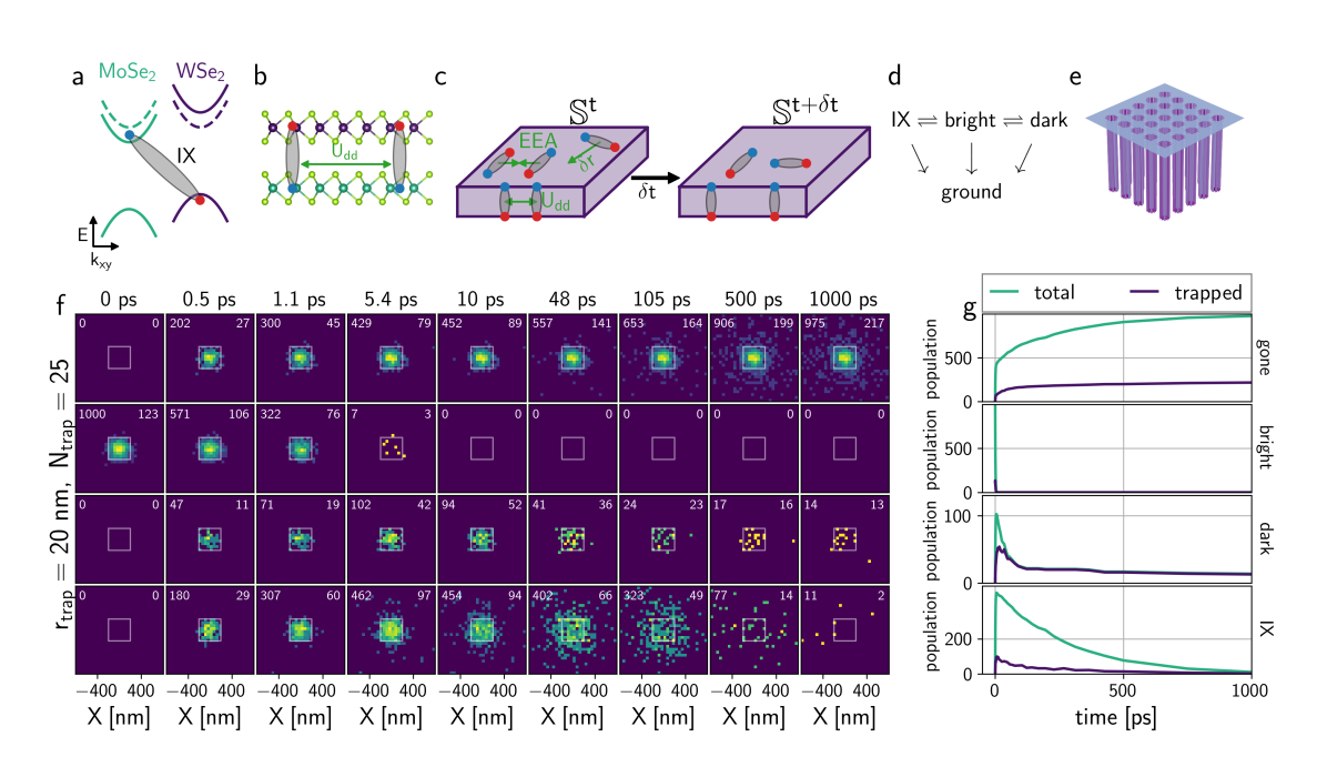
To reflect the associated photodynamic processes during the lifetimes of IXs, we explicitly consider exciton diffusion, recombination, trapping, bright-dark flipping, and exciton-exciton-annihilation (EEA) on an equal footing with the formation and dipole-dipole interaction of IXs (Figure 1c,d). To a first approximation, we neglect the influences of exciton complexes and exciton-exciton correlations. A discrete-time random walk of fixed step size provides an excellent description of exciton diffusion phenomena while simultaneously incorporating the other statistical processes. A full explanation of the model used in this study is given in the Supporting Information along with the parameters we use to simulate a MoSe2/WSe2 heterostructure (Table S1). A brief description of the model is given below and sketched in Figure 1c,d.
-
(i)
The evolution of the set of random walkers, , from time to is defined by the updating schema
(1) in which is constructed from functional, stochastic, sub-propagators that are defined to account for physical processes such as diffusion, recombination, EEA and dipole-dipole repulsion.
-
(ii)
At each time step, movement is accomplished for each element of by which moves each exciton a specific distance, , with a random angle, , drawn from a uniform distribution
(2) The spatial stepsize is held constant and calculated from the diffusivity in two-dimensions, ,
(3) -
(iii)
Hopping into and out of traps is controlled by diffusion and a Miller-Abrahams probability weighting factor,[34]
(4) which yields the moving probability being dependent on the relative energies of the current and proposed new locations for each exciton.
-
(iv)
To account for the trapping-induced changes in the recombination lifetimes, ,[18, 22, 35] we adapt the concept of 2D exciton coherence area which is determined by exciton scattering.[36, 37] From this model, we find that the exciton radiative lifetime is dependent on the exciton coherence radius , oscillator strength , and temperature ,
(5) with being a collection of constants directly related to the material, and being the exciton’s reduced mass. During our calculations, is set to the trap radius, , if an exciton is in a trap. The oscillator strengths are chosen to emulate radiative lifetimes found in the literature with (see Table S1 for the detailed parameters).
-
(v)
The EEA process typically happens on ultrafast time scales in quantum confined semiconductors and is one of the major parasitic mechanisms in diminishing exciton populations.[38, 39] In our model, it is considered to occur when two excitons are within a certain annihilation capture radius, which results in the stochastic annihilation of one of the excitons and the remaining one being moved to their joint Euclidean mid-point.
-
(vi)
The strong dipole-dipole repulsive interactions among IXs with dipole, , separated by a pair distance ,
(6) are implemented by using a mean-field approach. The change in the dipole potential energies caused by dipole-dipole interactions as an IX moves a distance
(7) is incorporated into the Miller-Abrahams hopping rates. Here, is the mean-field force caused by all pair-potential dipole interactions,
- (vii)
III Results and Discussion
To exemplify the workflow of our simulation, we consider an array of 55 () flat-bottomed potential traps that are 20 nm in radius ( nm) and equally separated by 50 nm (Figure 1e) at 5 K. The depths of the potential traps, , are set to be 50 meV. An instantaneous, diffraction limited Gaussian pulse with a full-width-at-half-maximum of 215 nm centered at the trap array populates an initial exciton number of into the bright intralayer exciton state. This excitation condition corresponds to an initial density of 21012 excitons per cm2 in the diffraction-limited excitation spot. The spatial dimensions of the simulation are not bounded, however the temporal dimension is bounded to [0,5] ns (100000 steps).
Figure 1f shows time slices of these photogenerated excitons. The rows correspond to different types of excitons: decayed excitons including both intralayer and interlayer excitons (“gone”), bright intralayer excitons (“bright”), dark intralayer excitons (“dark”), and interlayer excitons (“IX”). The total number of the specific exciton type still “living” at that moment is shown in the top left corner of each frame while the number of the corresponding trapped excitons is in the top right corner. Figure 1g presents the total and trapped populations of each exciton type at each time point of the simulation shown in Figure 1f.
At time = 0, 1000 bright intralayer excitons are generated, followed by their recombination or diffusion (Figure 1f and 1g, second row). Alternatively, the bright intralayer excitons can also convert to dark intralyer excitons (Figure 1f and 1g, third row) or IXs (Figure 1f and 1g, bottom row), which all eventually transition to the ground state (Figure 1f and 1g, top row). Once an exciton has converted to the ground state, it is no longer propagated. For simplicity, in the following, we refer to the bright (dark) intralayer excitons as the bright (dark) excitons. While the consumption of the bright excitons occurs within the first 5 ps, consistent with previous reports,[40] the build up of free and trapped dark and interlayer excitons and their subsequent decay happens over hundreds of picoseconds (Figure 1g). Diffusion of the free IXs is clearly evident in the evolution of the IX frames of Figure 1f (bottom row); these frames track the locations of the IXs before they decay to the ground state.
In order to quantify the trapping efficiency for a given set of simulation conditions, we define a metric,
| (8) |
in which and are the total and trapped number of “living” IXs, respectively, at a given simulation time point . Their time evolution curves are shown in Figure 1g (bottom row). is unity when all IXs are trapped during the entire simulation and less than unity when some IXs are not trapped. This value gives a time- and trap-averaged evaluation of the trapping capability throughout the lifetimes of the IXs. Note that this metric can be applied to other types of excitons, but in the main text we exclusively apply it to the IXs. Another important measure of the trapping behavior is the average number of IXs localized per potential trap before they undergo recombination, . Since an IX may experience multiple trapping and detrapping throughout its lifetime, we use the maximum number of trapped IXs divided by the trap number as an estimation of . For the specific example shown in Figure 1g (bottom row) we find . In the following, we systematically investigate the influence of different parameters, including the trap geometries and temperature, on the trapping properties of the IXs.
III.1 Influence of the potential trap size
Since the size of the potential traps directly defines the inter-exciton distances and their interactions, which can be manifested as the number of excitons per trap, we start by investigating the influence of the trap size on the IX trapping properties. During the simulation, we constrain ourselves to conditions which are experimentally relevant, i.e. trap sizes that are comparable to those created by strains, defects, and moiré potentials.[41, 42, 20, 19] Five potential landscapes of trap arrays with radii of 100 nm, 20 nm, 11 nm, 5 nm and 2.5 nm are constructed (Figure 2a). For ease of comparison, all of these primary trap potentials have the same total area. Hence, a total of = 1, 25, 81, 400, and 1600 traps are simulated, respectively. We conceptualize the different trap radii as moving from microscopic traps which can be created by strains[18, 24] to nanoscopic traps caused by atomic defects or moiré potentials.[17, 43] Aside from the trap size, all the other simulation conditions are kept constant: temperature = 5 K, trap depth = 50 meV and initial exciton population . Since under these conditions, the trap shape has no pronounced influence on the IX trapping behavior (Figure S3), we focus our discussion on the flat-bottom shaped potential traps.
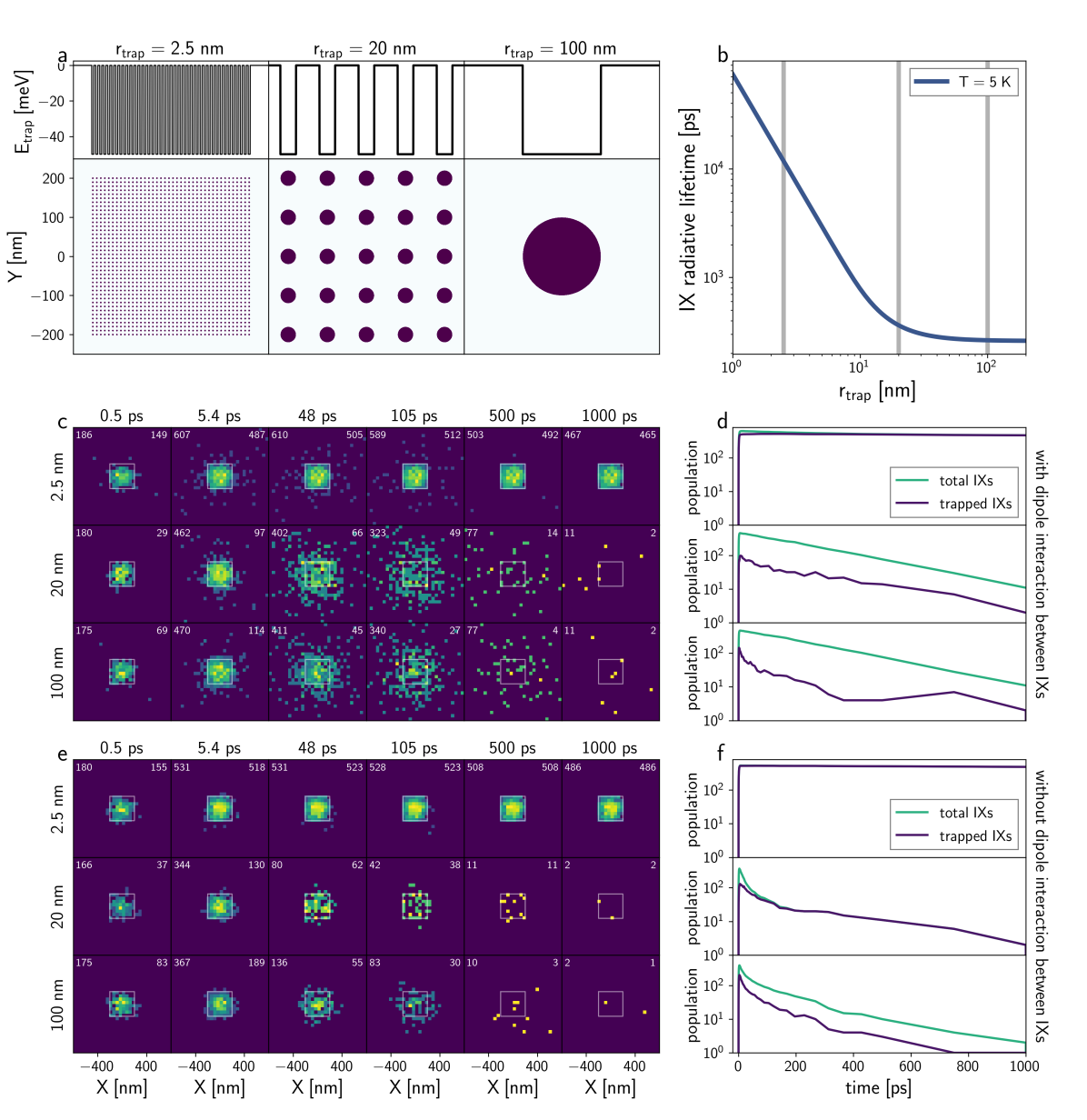
Figure 2c and Figure 2d shows the evolution of the “living” IXs in three potential trap arrays with various radii before they decay to the ground state. An apparent reduction in the lifetimes of the trapped IXs can be observed when the trap size increases from 2.5 nm to 100 nm. We believe the reason for the observed lifetime shortening is two fold. Firstly, as the size of the potential trap increases, the extent of quantum confinement experienced by the trapped IXs in the lateral dimension reduces. From a trap size of 2.5 nm to 100 nm, the quantum confinement transitions from two-dimensional to one-dimensional, considering that the Bohr radius of the IXs is a few nanometers.[43]. By adopting an exciton coherent motion area model that have been widely used to describe two-dimensional (2D) excitons,[36, 37] in which the transition oscillator strength of an exciton is assumed to be equivalent to the sum of the oscillator strengths of all the unit cells that contribution to the optical transitions, we find that the recombination lifetime of the trapped IXs reduces with increasing trap size (Figure 2b). Secondly, an increase in the trap size may result in multiple IXs in the same potential trap, hence increasing the possibility of the EEA process. This scenario is supported by evaluating the average number of IXs localized per potential trap, . As shown in Figure 3b, the value of increases from an average of less than one IX per trap for the 2.5 nm sized traps to more than 100 IXs for the 100 nm sized traps. Apparently, IXs trapped in the latter would experience EEA processes more frequently.
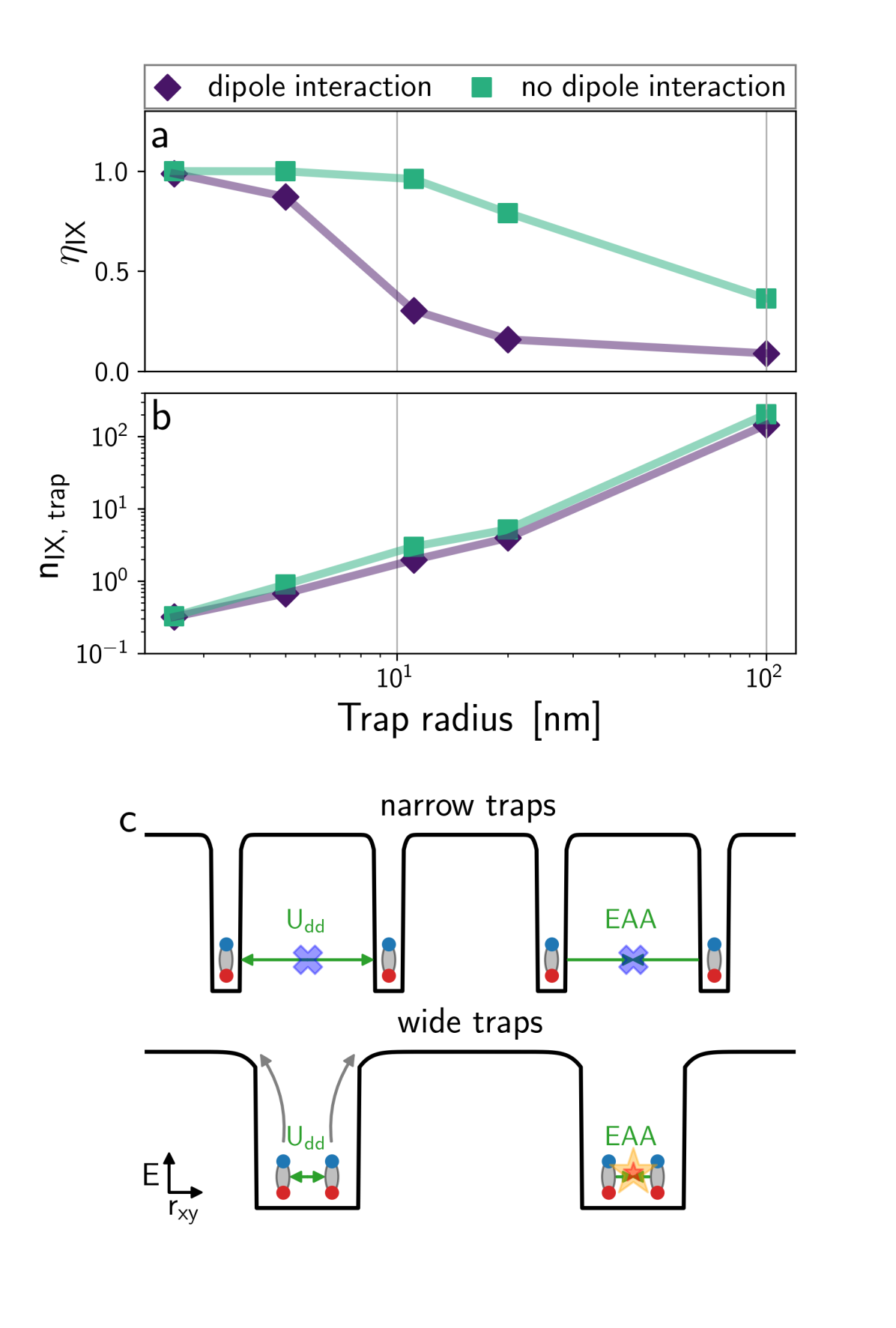
To understand the trap size-dependent IX localization behavior, we further inspect the trapping efficiency of the IXs as a function of the trap size (Figure 3a). While an array of 2.5 nm sized traps has a near unity trapping efficiency, that of the 100 nm sized trap is decreased by an order of magnitude to only around 10. The most significant reduction occurs when the trap size is between 5 nm to 20 nm. This is in stark contrast to the trapping efficiency of the dark excitons, which exhibit respectable trapping efficiencies for all of the various sized traps (Figure S5). Because of the long lifetimes of the IXs and dark excitons, it is temping to think of the IXs merely as long-lived intralayer excitons similar to dark excitons. However, the characteristic out-of-plane permanent dipole moment and the resultant dipole-dipole repulsion of the IXs distinguish them from intralayer excitons. We believe these unique features of the IXs are the primary reasons for the drastically different trapping efficiencies of the IXs and dark excitons despite their similar long lifetimes.
Figure 2e,f presents the evolution of the IXs when the dipole-dipole repulsion term is turned off in the simulation. The behavior of the 2.5 nm trap simulation with dipole interactions on and off are nearly identical. Conversely, the larger trap systems have far fewer IXs at times greater than a few ps when the dipole interaction is removed. Without the dipole interaction, the IXs that do exist undergo far less stochastic movement (diffusion). Figure 3a shows that removing the dipole interaction leads to much greater trapping efficiency for large traps, however, the maximum number of excitons per trap, Figure 3b, is only slightly increased by turning off the dipole interaction. In other words, the dipole interaction enables IXs in systems with large traps to remain trapped for longer times but does not change the maximum number of IXs in traps around a picosecond after excitation.
Based on the fact that reducing the trap size drastically increases trapping efficiencies of the IXs by taking into account dipole-dipole repulsion (Figure 3a), we speculate that with myriad narrow traps, each IX has its own trap and is therefore isolated from inter-IX interactions like dipole repulsion and EEA. However, when wide traps are present, multiple IXs congregate in each trap and they can either push each other out of the trap via dipolar interactions or the total lifetime of the ensemble can be decreased because of EEA process. We confirm this speculation by simulating the time evolution of the number of IXs in each trap (Figure S10). While a significant portion of the 20 nm sized traps can host more than 10 IXs during the initial few picoseconds after the photoexcitation, the number of IXs trapped in the 2.5 nm sized traps is predominantly one or none. Additionally, Figure S10 and S11 demonstrate that when a 2.5 nm trap becomes doubly occupied, the next time step it is not occupied at all–indicating that doubly occupied traps enhance EEA and IX ejection via the dipole interaction. We schematically illustrate these ideas in Figure 3c.
These findings explain the sudden start of reduction in the IX trapping efficiency when the dipole-dipole repulsion is included and the trap size is between 5 nm to 20 nm (Figure 3a): the dipole-dipole repulsion is most effective when the inter-IX distance is a few nanometers due to the scaling of the dipole force (Equation S34). More importantly, these results underscore the optimal conditions for localizing individual IXs in potential traps: it is critical to have small traps that are a few nanometers in size. This finding agrees well with the recent observations of single IXs localized in a moiré potential trap[43] and multiple IXs in strain-induced traps[18]: while both types of potential traps may offer similar trapping depths, the moiré potential traps are typically a few nanometers in size,[43, 17] significantly smaller than the strain-induced traps[42], and thus allow the localization of individual IXs.
III.2 Influence of the exciton density
We further interrogate the influence of exciton density on the trapping behavior of the IXs. For ease of comparison, we keep the system temperature at 5 K, the trap depth at 50 meV, and the trap radius at 20 nm. The initial bright, intralayer exciton population is varied between 125 and 4000, while the number of traps is tuned from 4 to 36. In this way, we constrain the initial exciton density to below 1013 cm-2 because at higher densities, the free IX picture may no longer be valid and instead, degenerate electron-hole plasmas can form.[44]
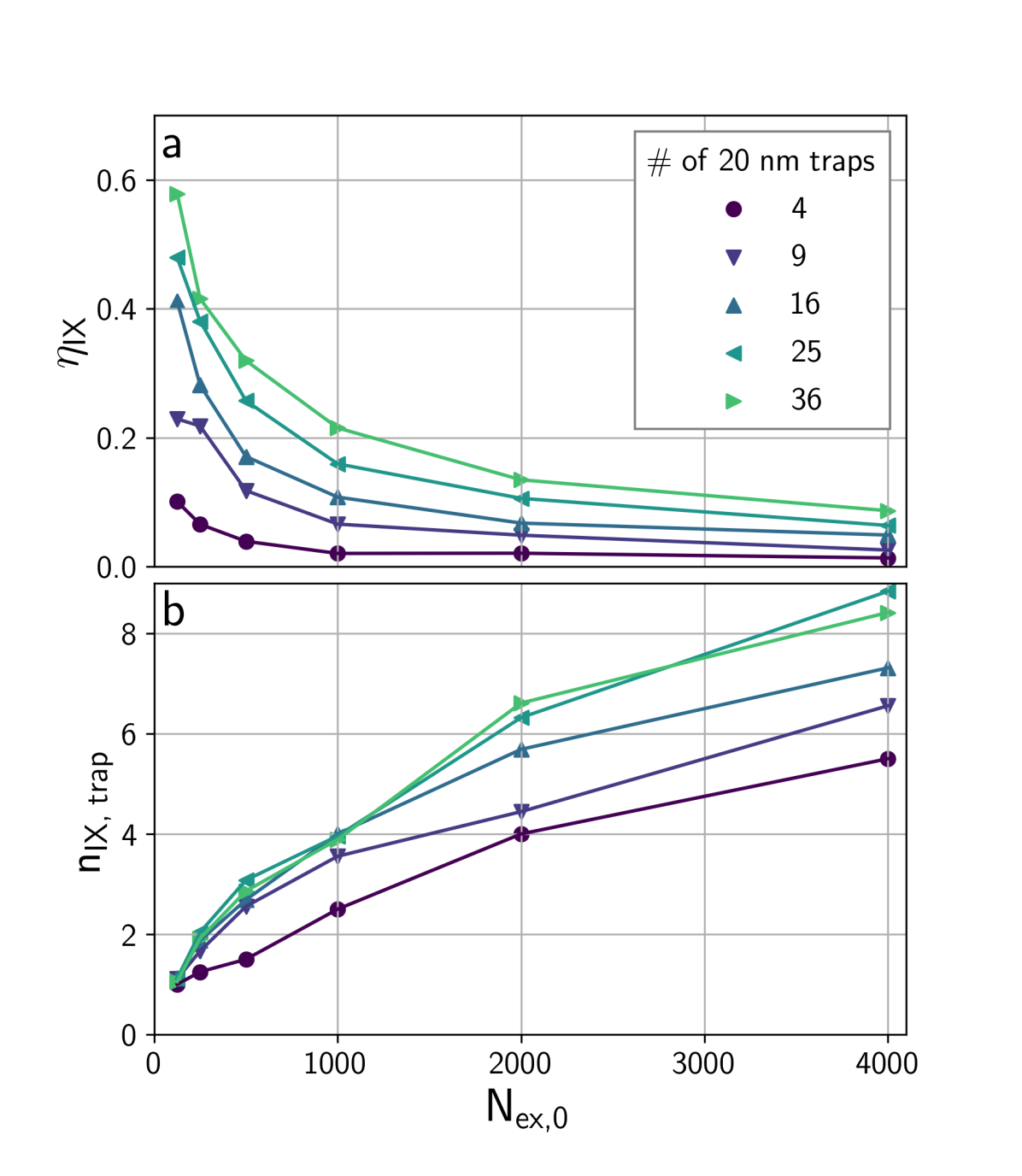
Figure 4a shows that a reduction in the initial exciton density (i.e. exciton population per trap), whether through decreasing the initial exciton population or increasing the trap number , leads to an increase in the IX trapping efficiency. Similar results can be observed for 2.5 nm sized potential traps (Figure S8), although the relative trapping efficiency is considerably higher. We believe the reason for this exciton density-dependent trapping behavior is the same as that shown in Figure 3c: populating the same potential trap with multiple IXs would result in their strong repulsive interactions. As a consequence, some of the IXs get pushed out of the traps, leading to less efficient trapping at higher exciton densities. Additionally, Figure 4b shows that increasing the initial exciton density causes to increase. The relationship between and initial density is sub-linear at large densities indicating a significant saturation behavior. Seemingly, a larger number of traps moves the saturation onset to larger densities. These observations are consistent with previously observed exciton density-dependent IX transport, in which the effect of the moiré potential was screened at high exciton densities.[17, 45] Indeed, Wang et al. [44] experimentally observed a moiré trapped-IX to free-IX gas transition in MoSe2/WSe2 at IX densities (1011 cm-2) in the same range which we investigate here.
III.3 Influence of temperature and trap depth
One of the most appealing properties of the IXs in TMDs when compared to indirect excitons in traditional semiconductor heterostructures is their large binding energy,[11, 12] which may open many opportunities for TMD-based quantum photonic and optoelectronic devices operating at elevated temperatures. For example, quantum photon sources that function at room temperature may offer many technical advantages.[46, 47] Recent experimental and theoretical studies have suggested the possibility of realizing high temperature exciton condensation and superconductivity based on IXs in TMDs.[5, 10, 48] An understanding of temperature- and trap depth-dependent IX trapping in TMD heterostructures is of high practical relevance.
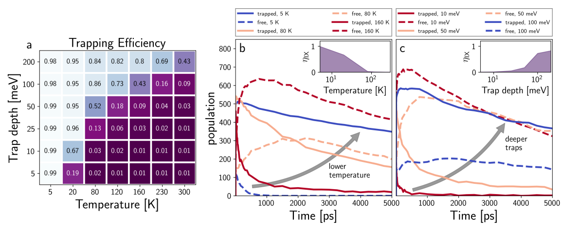
The influences of the system temperature and trap depth are investigated by varying the former in the range of 5 - 300 K and the latter in the range of 5 - 200 meV while maintaining the same trap area and bright exciton density of 1000. This trap depth range is representative of experimentally obtainable values: strain-induced traps typically have depths of a few tens to a few hundreds of meV,[41, 42, 22, 49] while that of moiré potentials can be a few hundreds of meV.[50] We find that increasing the system temperature reduces the trapping efficiency (Figure 5a). A similar reduction phenomenon can be observed when the trap depth is reduced, although to a much lesser extent. For an increase in the trap depth, a consistent increase in the trapping efficiency can be observed until a plateau is reached, which defines the maximum achievable IX trapping efficiency by optimizing the trap depth while keeping the other parameters the same. A similar trend is observed for 20 nm radii traps (Figure S6b).
For 50 meV deep 2.5 nm radii traps, Figure 5b shows that at 5 K trapped IXs have a far greater population than free IXs. As the temperature is increased, the dominant population flips between 80 and 160 K. This change in dominant species is analogous to the trapped-to-free-gas transition observed by Wang et al. [44]. Fixing the temperature at 120 K and changing the trap depth (Figure 5c) demonstrates that a similar flip between the dominant population happens at a trap depth between 50 and 100 meV. The thermodynamic controls of temperature and trap depth therefore not only have jurisdiction over temporally integrated behavior like trapping efficiency (Figure 5a, which relate to steady-state device performances); these controls also have a rich interplay with each other to define the ultrafast evolution of the IX populations and whether the dominant species is trapped or a freely diffusing gas.
IV Conclusions
Using a discrete-time random walk model, we study the trapping behavior of IXs in TMD heterostructures. By systematically investigating the influences of trap parameters such as size and depth and externally controlled parameters like system temperature and exciton density, we are able to illustrate conditions when IX localization should be expected. We find that dipolar repulsion among IXs distinguishes them from intralayer excitons and has a strong impact on their trapping. This is manifested as low trapping efficiencies of IXs in large traps, in which dipole-dipole repulsion helps push IXs out of the traps. In contrast, nanoscale traps afforded by pointed defects and moiré potentials are most effective in localizing the IXs—high densities of trapped IXs are achievable when sufficient deep traps are provided for each IX to be separated from its neighbor. The same mechanism is also reflected in the low trapping efficiencies at high exciton densities, where increases in dipolar repulsive interactions effectively screen the effect of the potential traps. We also show that temperature and trap depth form a rich control system for defining whether the dominant IX population is trapped or free. These results indicate the importance of engineering nanoscale traps such as point defects and moiré potentials in order to effectively trap IXs for quantum photonic applications.
V Supporting Information
The Supporting Information is available free of charge at URL and includes computational methods, results demonstrating the role of trap shape and dark excitons, and a discussion of individual trap occupancy.
Acknowledgements.
This work was performed, in part, at the Center for Nanoscale Materials, a U.S. Department of Energy Office of Science User Facility, and supported by the U.S. Department of Energy, Office of Science, under Contract No. DE-AC02-06CH11357. X.M. acknowledges support by the Department of Energy, Center for Molecular Quantum Transduction Energy Frontier Research Center, under Grant No. DE-SC0021314.References
- Rivera et al. [2015] P. Rivera, J. R. Schaibley, A. M. Jones, J. S. Ross, S. Wu, G. Aivazian, P. Klement, K. Seyler, G. Clark, N. J. Ghimire, J. Yan, D. G. Mandrus, W. Yao, and X. Xu, Observation of long-lived interlayer excitons in monolayer MoSe2–WSe2 heterostructures, Nat. Commun. 6, 6242 (2015).
- Ciarrocchi et al. [2018] A. Ciarrocchi, D. Unuchek, A. Avsar, K. Watanabe, T. Taniguchi, and A. Kis, Polarization switching and electrical control of interlayer excitons in two-dimensional van der waals heterostructures, Nat. Photon. 13, 131 (2018).
- Karni et al. [2019] O. Karni, E. Barré, S. C. Lau, R. Gillen, E. Y. Ma, B. Kim, K. Watanabe, T. Taniguchi, J. Maultzsch, K. Barmak, R. H. Page, and T. F. Heinz, Infrared interlayer exciton emission in MoS2/WSe2 heterostructures, Phys. Rev. Lett. 123, 247402 (2019).
- Butov et al. [2001] L. V. Butov, A. L. Ivanov, A. Imamoglu, P. B. Littlewood, A. A. Shashkin, V. T. Dolgopolov, K. L. Campman, and A. C. Gossard, Stimulated scattering of indirect excitons in coupled quantum wells: Signature of a degenerate Bose-gas of excitons, Phys. Rev. Lett. 86, 5608 (2001).
- Wang et al. [2019] Z. Wang, D. A. Rhodes, K. Watanabe, T. Taniguchi, J. C. Hone, J. Shan, and K. F. Mak, Evidence of high-temperature exciton condensation in two-dimensional atomic double layers, Nature 574, 76 (2019).
- Lukin et al. [2001] M. D. Lukin, M. Fleischhauer, R. Cote, L. M. Duan, D. Jaksch, J. I. Cirac, and P. Zoller, Dipole blockade and quantum information processing in mesoscopic atomic ensembles, Phys. Rev. Lett. 87, 037901 (2001).
- Paik et al. [2019] E. Y. Paik, L. Zhang, G. W. Burg, R. Gogna, E. Tutuc, and H. Deng, Interlayer exciton laser of extended spatial coherence in atomically thin heterostructures, Nature 576, 80 (2019).
- Combescot et al. [2017] M. Combescot, R. Combescot, and F. Dubin, Bose–einstein condensation and indirect excitons: a review, Rep. Prog. Phys. 80, 066501 (2017).
- High et al. [2012] A. A. High, J. R. Leonard, M. Remeika, L. V. Butov, M. Hanson, and A. C. Gossard, Condensation of excitons in a trap, Nano Lett. 12, 2605 (2012).
- Fogler et al. [2014] M. M. Fogler, L. V. Butov, and K. S. Novoselov, High-temperature superfluidity with indirect excitons in van der waals heterostructures, Nat. Commun. 5, 4555 (2014).
- Gillen and Maultzsch [2018] R. Gillen and J. Maultzsch, Interlayer excitons in MoSe2/WSe2 heterostructures from first principles, Phys. Rev. B 97, 165306 (2018).
- der Donck and Peeters [2018] M. V. der Donck and F. M. Peeters, Interlayer excitons in transition metal dichalcogenide heterostructures, Phys. Rev. B 98, 115104 (2018).
- Zhang et al. [2019] J. Zhang, L. Du, S. Feng, R.-W. Zhang, B. Cao, C. Zou, Y. Chen, M. Liao, B. Zhang, S. A. Yang, G. Zhang, and T. Yu, Enhancing and controlling valley magnetic response in MoS2/WS2 heterostructures by all-optical route, Nat. Commun. 10, 4226 (2019).
- High et al. [2009] A. A. High, A. K. Thomas, G. Grosso, M. Remeika, A. T. Hammack, A. D. Meyertholen, M. M. Fogler, L. V. Butov, M. Hanson, and A. C. Gossard, Trapping indirect excitons in a gaas quantum-well structure with a diamond-shaped electrostatic trap, Phys. Rev. Lett. 103, 087403 (2009).
- Yoshioka et al. [2011] K. Yoshioka, E. Chae, and M. Kuwata-Gonokami, Transition to a Bose–Einstein condensate and relaxation explosion of excitons at sub-kelvin temperatures, Nat. Commun. 2, 328 (2011).
- Remeika et al. [2009] M. Remeika, J. C. Graves, A. T. Hammack, A. D. Meyertholen, M. M. Fogler, L. V. Butov, M. Hanson, and A. C. Gossard, Localization-delocalization transition of indirect excitons in lateral electrostatic lattices, Phys. Rev. Lett. 102, 186803 (2009).
- Yuan et al. [2020] L. Yuan, B. Zheng, J. Kunstmann, T. Brumme, A. B. Kuc, C. Ma, S. Deng, D. Blach, A. Pan, and L. Huang, Twist-angle-dependent interlayer exciton diffusion in WS2–WSe2 heterobilayers, Nat. Mater. 19, 617 (2020).
- Wang and Ma [2020] W. Wang and X. Ma, Strain-induced trapping of indirect excitons in MoSe2/WSe2 heterostructures, ACS Photonics 7, 2460 (2020).
- Shanks et al. [2021] D. N. Shanks, F. Mahdikhanysarvejahany, C. Muccianti, A. Alfrey, M. R. Koehler, D. G. Mandrus, T. Taniguchi, K. Watanabe, H. Yu, B. J. LeRoy, and J. R. Schaibley, Nanoscale trapping of interlayer excitons in a 2D semiconductor heterostructure, Nano Lett. 10.1021/acs.nanolett.1c01215 (2021).
- Wu et al. [2018] F. Wu, T. Lovorn, and A. H. MacDonald, Theory of optical absorption by interlayer excitons in transition metal dichalcogenide heterobilayers, Phys. Rev. B 97, 035306 (2018).
- Imamoḡlu et al. [1997] A. Imamoḡlu, H. Schmidt, G. Woods, and M. Deutsch, Strongly interacting photons in a nonlinear cavity, Phys. Rev. Lett. 79, 1467 (1997).
- Peng et al. [2020] L. Peng, H. Chan, P. Choo, T. W. Odom, S. K. R. S. Sankaranarayanan, and X. Ma, Creation of single-photon emitters in WSe2 monolayers using nanometer-sized gold tips, Nano Lett. 20, 5866 (2020).
- Baek et al. [2020] H. Baek, M. Brotons-Gisbert, Z. X. Koong, A. Campbell, M. Rambach, K. Watanabe, T. Taniguchi, and B. D. Gerardot, Highly energy-tunable quantum light from moiré-trapped excitons, Sci. Adv. 6, eaba8526 (2020).
- Kremser et al. [2020] M. Kremser, M. Brotons-Gisbert, J. Knörzer, J. Gückelhorn, M. Meyer, M. Barbone, A. V. Stier, B. D. Gerardot, K. Müller, and J. J. Finley, Discrete interactions between a few interlayer excitons trapped at a MoSe2–WSe2 heterointerface, npj 2D Mater Appl 4, 8 (2020).
- Cho et al. [2021] C. Cho, J. Wong, A. Taqieddin, S. Biswas, N. R. Aluru, S. Nam, and H. A. Atwater, Highly strain-tunable interlayer excitons in MoS2/WSe2 heterobilayers, Nano Lett. 21, 3956 (2021).
- Ovesen et al. [2019] S. Ovesen, S. Brem, C. Linderälv, M. Kuisma, T. Korn, P. Erhart, M. Selig, and E. Malic, Interlayer exciton dynamics in van der waals heterostructures, Commun. Phys. 2, 23 (2019).
- Ceballos et al. [2014] F. Ceballos, M. Z. Bellus, H.-Y. Chiu, and H. Zhao, Ultrafast charge separation and indirect exciton formation in a MoS2–MoSe2 van der waals heterostructure, ACS Nano 8, 12717 (2014).
- Harats and Bolotin [2020] M. G. Harats and K. I. Bolotin, Limits of funneling efficiency in non-uniformly strained 2D semiconductors, 2D Materials 8, 015010 (2020).
- Li et al. [2021] Z. Li, X. Lu, D. F. C. Leon, Z. Lyu, H. Xie, J. Hou, Y. Lu, X. Guo, A. Kaczmarek, T. Taniguchi, K. Watanabe, L. Zhao, L. Yang, and P. B. Deotare, Interlayer exciton transport in MoSe2/WSe2 heterostructures, ACS Nano 15, 1539 (2021).
- Yuan et al. [2017] L. Yuan, T. Wang, T. Zhu, M. Zhou, and L. Huang, Exciton dynamics, transport, and annihilation in atomically thin two-dimensional semiconductors, J. Phys. Chem. Lett. 8, 3371 (2017).
- Echeverry et al. [2016] J. P. Echeverry, B. Urbaszek, T. Amand, X. Marie, and I. C. Gerber, Splitting between bright and dark excitons in transition metal dichalcogenide monolayers, Phys. Rev. B 93, 121107 (2016).
- Harris et al. [2020] C. R. Harris, K. J. Millman, S. J. van der Walt, R. Gommers, P. Virtanen, D. Cournapeau, E. Wieser, J. Taylor, S. Berg, N. J. Smith, R. Kern, M. Picus, S. Hoyer, M. H. van Kerkwijk, M. Brett, A. Haldane, J. F. del Río, M. Wiebe, P. Peterson, P. Gérard-Marchant, K. Sheppard, T. Reddy, W. Weckesser, H. Abbasi, C. Gohlke, and T. E. Oliphant, Array programming with NumPy, Nature 585, 357 (2020).
- Lam et al. [2015] S. K. Lam, A. Pitrou, and S. Seibert, Numba: A llvm-based python jit compiler, in Proceedings of the Second Workshop on the LLVM Compiler Infrastructure in HPC (2015) pp. 1–6.
- Miller and Abrahams [1960] A. Miller and E. Abrahams, Impurity conduction at low concentrations, Phys. Rev 120, 745 (1960).
- Srivastava et al. [2015] A. Srivastava, M. Sidler, A. V. Allain, D. S. Lembke, A. Kis, and A. Imamoğlu, Optically active quantum dots in monolayer WSe2, Nat. Nanotechnol 10, 491 (2015).
- Feldmann et al. [1987] J. Feldmann, G. Peter, E. O. Göbel, P. Dawson, K. Moore, C. Foxon, and R. J. Elliott, Linewidth dependence of radiative exciton lifetimes in quantum wells, Phys. Rev. Lett. 59, 2337 (1987).
- Ma et al. [2017] X. Ma, B. T. Diroll, W. Cho, I. Fedin, R. D. Schaller, D. V. Talapin, S. K. Gray, G. P. Wiederrecht, and D. J. Gosztola, Size-dependent biexciton quantum yields and carrier dynamics of quasi-two-dimensional core/shell nanoplatelets, ACS Nano 11, 9119 (2017).
- Mouri et al. [2014] S. Mouri, Y. Miyauchi, M. Toh, W. Zhao, G. Eda, and K. Matsuda, Nonlinear photoluminescence in atomically thin layered WSe2 arising from diffusion-assisted exciton-exciton annihilation, Phys. Rev. B 90, 155449 (2014).
- Ma et al. [2015a] X. Ma, O. Roslyak, J. G. Duque, X. Pang, S. K. Doorn, A. Piryatinski, D. H. Dunlap, and H. Htoon, Influences of exciton diffusion and exciton-exciton annihilation on photon emission statistics of carbon nanotubes, Phys. Rev. Lett. 115, 017401 (2015a).
- Hong et al. [2014] X. Hong, J. Kim, S.-F. Shi, Y. Zhang, C. Jin, Y. Sun, S. Tongay, J. Wu, Y. Zhang, and F. Wang, Ultrafast charge transfer in atomically thin MoS2/WS2 heterostructures, Nat. Nanotechnol. 9, 682 (2014).
- Darlington et al. [2020] T. P. Darlington, C. Carmesin, M. Florian, E. Yanev, O. Ajayi, J. Ardelean, D. A. Rhodes, A. Ghiotto, A. Krayev, K. Watanabe, T. Taniguchi, J. W. Kysar, A. N. Pasupathy, J. C. Hone, F. Jahnke, N. J. Borys, and P. J. Schuck, Imaging strain-localized excitons in nanoscale bubbles of monolayer WSe2 at room temperature, Nat. Nanotechnol. 15, 854 (2020).
- Rosenberger et al. [2019] M. R. Rosenberger, C. K. Dass, H.-J. Chuang, S. V. Sivaram, K. M. McCreary, J. R. Hendrickson, and B. T. Jonker, Quantum calligraphy: Writing single-photon emitters in a two-dimensional materials platform, ACS Nano 13, 904 (2019).
- Li et al. [2020] W. Li, X. Lu, S. Dubey, L. Devenica, and A. Srivastava, Dipolar interactions between localized interlayer excitons in van der waals heterostructures, Nat. Mater. 19, 624 (2020).
- Wang et al. [2021] J. Wang, Q. Shi, E.-M. Shih, L. Zhou, W. Wu, Y. Bai, D. Rhodes, K. Barmak, J. Hone, C. Dean, and X.-Y. Zhu, Diffusivity reveals three distinct phases of interlayer excitons in MoSe2/WSe2 heterobilayers, Phys. Rev. Lett. 126, 106804 (2021).
- Seyler et al. [2019] K. L. Seyler, P. Rivera, H. Yu, N. P. Wilson, E. L. Ray, D. G. Mandrus, J. Yan, W. Yao, and X. Xu, Signatures of moiré-trapped valley excitons in MoSe2/WSe2 heterobilayers, Nature 567, 66 (2019).
- Tran et al. [2016] T. T. Tran, K. Bray, M. J. Ford, M. Toth, and I. Aharonovich, Quantum emission from hexagonal boron nitride monolayers, Nat. Nanotechnol. 11, 37 (2016).
- Ma et al. [2015b] X. Ma, N. F. Hartmann, J. K. S. Baldwin, S. K. Doorn, and H. Htoon, Room-temperature single-photon generation from solitary dopants of carbon nanotubes, Nat. Nanotechnol. 10, 671 (2015b).
- Lu et al. [2018] J. Lu, O. Zheliuk, Q. Chen, I. Leermakers, N. E. Hussey, U. Zeitler, and J. Ye, Full superconducting dome of strong ising protection in gated monolayer WS2, Proceedings of the National Academy of Sciences 115, 3551 (2018).
- Branny et al. [2017] A. Branny, S. Kumar, R. Proux, and B. D. Gerardot, Deterministic strain-induced arrays of quantum emitters in a two-dimensional semiconductor, Nat. Commun 8, 15053 (2017).
- Zhang et al. [2017] C. Zhang, C.-P. Chuu, X. Ren, M.-Y. Li, L.-J. Li, C. Jin, M.-Y. Chou, and C.-K. Shih, Interlayer couplings, moiré patterns, and 2D electronic superlattices in MoS2/WSe2 hetero-bilayers, Sci. Adv. 3, e1601459 (2017).