Lightweight Hardware Transform Design for the Versatile Video Coding 4K ASIC Decoders
Abstract
Versatile Video Coding (VVC) is the next generation video coding standard finalized in July 2020. VVC introduces new coding tools enhancing the coding efficiency compared to its predecessor High Efficiency Video Coding (HEVC). These new tools have a significant impact on the VVC software decoder complexity estimated to 2 times HEVC decoder complexity. In particular, the transform module includes in VVC separable and non-separable transforms named Multiple Transform Selection (MTS) and Low Frequency Non-Separable Transform (LFNST) tools, respectively. In this paper, we present an area-efficient hardware architecture of the inverse transform module for a VVC decoder. The proposed design uses a total of 64 regular multipliers in a pipelined architecture targeting Application-Specific Integrated Circuit (ASIC) platforms. It consists in a multi-standard architecture that supports the transform modules of recent MPEG standards including Advanced Video Coding (AVC), HEVC and VVC. The architecture leverages all primary and secondary transforms’ optimisations including butterfly decomposition, coefficients zeroing and the inherent linear relationship between the transforms. The synthesized results show that the proposed method sustains a constant throughput of 1 sample per cycle and a constant latency for all block sizes. The proposed hardware inverse transform module operates at 600 MHz frequency enabling to decode in real-time 4K video at 30 frames per second in 4:2:2 chroma sub-sampling format. The proposed module has been integrated in an ASIC UHD decoder targeting energy-aware decoding of VVC videos on consumer devices.
Index Terms:
VVC decoder, Inverse Transform module, LFNST, MTS, DCT, DST and ASIC.I Introduction
The Versatile Video Coding (VVC) is the next generation video coding standard jointly developed by Motion Picture Experts Group (MPEG) and Video Coding Experts Group (VQEG) under the Joint Video Experts Team (JVET). VVC was finalized in July 2020 as ITU-T H.266 — MPEG-I - Part 3 (ISO/IEC 23090-3) standard [1, 2]. It introduces several new coding tools enabling up to 40% of coding gains beyond the High Efficiency Video Coding (HEVC) standard [3, 4]. The VVC transform module includes two new tools called Multiple Transform Selection (MTS) and Low Frequency Non-Separable Transform (LFNST) [5]. The MTS tool involves three trigonometrical transform types including Discrete Cosine Transform (DCT) type II (DCT-II), DCT type VIII (DCT-VIII) and Discrete Sine Transform (DST) type VII (DST-VII) with block sizes that can reach for DCT-II and for DCT-VIII and DST-VII. The use of DCT/DST families gives the ability to apply separable transforms, the transformation of a block can be applied separately in horizontal and vertical directions. Therefore, the VVC encoder selects a combination of horizontal and vertical transforms that minimizes the rate-distortion cost , computed in (1) as a trade-off between distortion and rate
| (1) |
where is a Lagrangian parameter computed depending on the quantisation parameter.
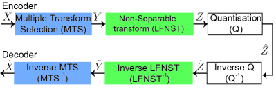
The LFNST is applied after the separable transform and before the quantisation at the encoder side. At the decoder side, it is applied after the inverse quantisation and before the inverse separable transform. Fig. 1 illustrates the VVC transform module at both encoder and decoder sides. The transform module relies on matrix multiplication with and computing complexities for separable and non-separable transforms, respectively. In terms of memory usage, the VVC transform module requires higher memory allocated to store the coefficients of the transform kernels: three kernels are defined for MTS and eight kernels for LFNST.
Fast computing algorithms for DCTs/DSTs have been widely investigated in the literature. The main objective of these algorithms is to perform the transform with the lowest number of multiplications compared to a naive matrix multiplication requiring for square matrix multiplications (ie. computational complexity). The DCT-II can be decomposed in butterfly [6, 7, 8] reducing computational complexity in terms of number of multiplications and additions. This decomposition is hardware-friendly enabling hardware resources sharing between blocks of different sizes for both computation and memory usage. In contrast to DCT-II, DST-VII/DCT-VIII have less efficient fast implementation algorithms [9, 10, 11] and dot not enable hardware resources sharing. Table I summarises the performance in terms of number of multiplications and additions of fast implementations of DCT-II and DST-VIII at different sizes .
| Transforms | ||||||||||||||||
| Ref. | + | All | Ref. | + | All | Ref. | + | All | Ref. | + | All | |||||
| DCT-II | [7] | [7] | [8] | [8] | ||||||||||||
| DCT-II (HEVC) | [12] | [12] | [12] | [12] | ||||||||||||
| DST-VII | [9] | [10] | ||||||||||||||
| DST-VII | [11] | [11] | [11] | [11] | ||||||||||||
| DST-VII | [13] | [13] | [13] | |||||||||||||
| Matrix Multip. | ||||||||||||||||
This paper addresses a hardware implementation of the VVC inverse transform module for Application-Specific Integrated Circuit (ASIC) platforms. To the best of our knowledge, this is the first hardware design that includes both separable and non-separable transforms supporting all block sizes. The proposed implementation relies on a shared multipliers architecture using 32 multipliers for the separable transform and the same for the non-separable one. It also exploits all recursion and decomposition properties of the considered transforms to optimize the hardware resources and speedup the design. The choice of the shared multipliers architecture was based on our previous study recently published by Farhat et al. [14]. This latter compares between two different hardware architectures for the MTS, one uses Regular Multipliers (RM) while the second uses Multiple Constant Multipliers (MCM). This study showed better performance for the RM based architecture compared to MCM one for this particular problem. The main objective of this paper is to propose an optimized hardware implementation of the VVC inverse transform blocks for ASIC decoder featuring many advantages:
-
•
Minimise the hardware area by leveraging all possible optimisations offered by the transforms.
-
•
Support all block sizes of both MTS and LFNST.
-
•
Support all recent MPEG standards including AVC, HEVC and VVC.
-
•
Scalable design enabling to enhance both throughput and latency by only increasing the considered number of regular multipliers.
The proposed VVC inverse transform hardware design is able to sustain a constant latency and throughput regardless the coding configuration and the tools selected by the encoder. We target a fixed throughput of 1 sample/cycle for the entire transformation process with 2 samples/cycle for the 1D separable transform (MTS) and a 2 samples/cycle for the non-separable transform (LFNST) while sustaining a fixed system latency for all transform sizes and types. This latter constraint is importance to accurately predict the performance of the process and facilitate chaining between transform blocks. The proposed inverse transform design has been successfully integrated into a hardware multi-standard ASIC decoder. This latter can be embedded on various consumer electronics devices such as mobiles phones, setup boxes, TVs, etc.
The rest of this paper is organized as follows. Section II presents the background on the VVC transform module including MTS and LFNST. The existing hardware implementations of the transforms module are presented in Section III. The proposed hardware implementations of MTS and LFNST blocks are investigated in Section IV. In Section V, the performance of the proposed hardware module is assessed in terms of speedup and hardware area. Finally, Section VI concludes the paper.
II Background
In this section we describe the VVC transform module including MTS and LFNST blocks.
II-A Separable transform module
The concept of separable 2D transform enables applying two 1D transforms separately in horizontal and vertical directions
| (2) |
where is the input residual matrix of size , and are horizontal and vertical transform matrices of sizes and , respectively. ”” stands for matrix multiplication.
The inverse 2D separable transform is expressed in (3).
| (3) |
The HEVC transform module involves the DCT-II for square blocks of size with and DST-VII for square block of size [12, 15]. The concept of transform competition allows testing different transforms and types to select the one that minimises the rate distortion cost. It enables adapting the transformation to the statistics of the encoded signal (ie. block of residuals). The transform competition has been investigated under HEVC standard [16, 17], and more recently under the Joint Exploration Model (JEM) software [18]. The JEM codec defines five trigonometrical transform types including DCT-II, V and VIII, and DST-I and VII. Adopting transform competition under the JEM brings significant coding efficiency enhancements estimated between and of bitrate reductions [18]. This coding gain is achieved at the expense of complexity overhead required to test the transform candidates at the encoder side. Moreover, additional memory is required at both encoder and decoder to store the coefficients of those transform kernels. To cope with the complexity issue, subsets of transform candidates are defined offline, and only a subset of transforms are tested at the encoder depending on the block partitioning and prediction configuration such as the block size and Intra prediction mode [18], respectively.
The MTS block in VVC involves three transform types including DCT-II, VIII and DST-VII. The kernels of DCT-II , DST-VII and DCT-VIII are derived from (4), (5) and (6), respectively.
| (4) |
with .
| (5) |
| (6) |
with and is the transform size.
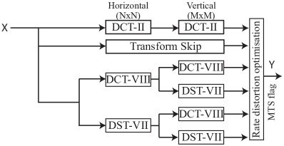
As illustrated in Fig. 2, the MTS concept selects, for Luma blocks of size lower than 64, a set of transforms that minimizes the rate distortion cost among five transform sets and the skip configuration. However, only DCT-II is considered for chroma components and Luma blocks of size 64. The sps_mts_enabled_flag flag defined at the Sequence Parameter Set (SPS) enables to activate the MTS concept at the encoder side. Two other flags are defined at the SPS level to signal whether implicit or explicit MTS signalling is used for Intra and Inter coded blocks, respectively. For the explicit signalling, used by default in the reference software, the tu_mts_idx syntax element signals the selected horizontal and vertical transforms as specified in Table II. This flag is coded with Truncated Rice code with rice parameter and (TRp). To reduce the computational cost of large block–size transforms, the effective height and width of the coding block (CB) are reduced depending of the CB size and transform type
| (7) |
| (8) |
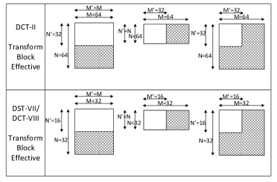
In (7) and (8), and are the effective width and height sizes, and are respectively the types of vertical and horizontal transforms (0: DCT-II, 1: DCT-VIII and 2: DST-VII), and the function returns the minimum between and . The sample value beyond the limits of the effective and are considered to be zero, thus reducing the computational cost of the 64-size DCT-II and 32-size DCT-VIII/DST-VII transforms. This concept is called zeroing in the VVC standard. Fig. 3 shows the possible zeroing scenarios for DCT-II and DCT-VIII/DST-VII transforms.
| tu_mts_idx | Transform Direction | |
| Horizontal Transform | Vertical Transform | |
| 0 | DCT-II | DCT-II |
| 1 | DST-VII | DST-VII |
| 2 | DCT-VIII | DST-VII |
| 3 | DST-VII | DCT-VIII |
| 4 | DCT-VIII | DCT-VIII |
II-B Non-separable transform module
The Low-Frequency Non-Separable Transform (LFNST) [19, 20] has been adopted in the VTM version 5. The LFNST relies on matrix multiplication applied between the forward primary transform and the quantisation at the encoder side:
| (9) |
where the vector includes the coefficients of the residual block rearranged in a vector and the matrix contains the coefficients transform kernel. The LFNST is enabled only when DCT-II is used as a primary transform. The inverse LFNST is expressed in (10).
| (10) |
Four sets of two LFNST kernels of sizes and are applied on 16 coefficients of small blocks (min (width, height) 8 ) and 64 coefficients of larger blocks (min (width, height) 4), respectively. The VVC specification defines four different transform sets selected depending on the Intra prediction mode and each set defines two transform kernels. The used kernel within a set is signalled in the bitstream. Table III gives the transform set index depending on the Intra prediction mode. The transform index within a set is coded with a Truncated Rice code with rice parameter and (TRp) and only the first bin is context coded. The LFNST is applied on Intra CU for both Intra and Inter slices and concerns Luma and Chroma components. Finally, LFNST is enabled only when DCT-II is used as primary transform.
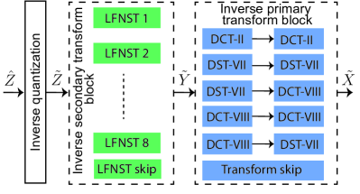
To reduce the complexity in number of operations and memory required to store the transform coefficients, the inverse transform is reduced to . Therefore, only 16 bases of the transform kernel are used and the number of input samples is reduced to 48 by excluding the bottom right block (ie. includes only samples of the top-left, top-right and bottom-left blocks). To further reduce the number of multiplications by sample, the LFNST restricts the transform of and blocks to and transforms, respectively. In those cases, the LFNST is applied only when the last significant coefficient is less than 8, and less than 16 for other block sizes. Fig. 4 illustrates the block diagram of the VVC inverse transform module.
The VVC transform module raises many challenges to the hardware implementation of the VVC decoder. The introduced DCT-II (p-64), DST-VII, DCT-VIII kernels with the 8 LFNST kernels will require high memory usage to store these coefficients. Moreover, these new transforms are more complex and require a higher number of multiplications as shown in Table I. Finally, the LFNST stage introduces an additional delay required to perform the secondary transform. Therefore, the hardware transform module should be carefully designed leveraging all optimisations to reach the target latency and throughput while minimising the hardware area.
| Intra Prediction Mode | Transform set index |
| 1 | |
| 0 | |
| 1 | |
| 2 | |
| 3 | |
| 2 | |
| 1 | |
| 0 |
III Related Work
In this section we give a brief description and analysis of existing hardware implementations of separable transforms proposed for HEVC and VVC.
III-A Hardware Implementations of DCT-II
DCT-II transform has been widely used by previous video coding standards such as Advanced Video Coding (AVC) [21] and HEVC. Therefore, its hardware implementation has been well studied and optimized for different architectures. Shen et al. [22] proposed a unified Very Large Scale Integration (VLSI) architecture for 4, 8, 16 and 32 point Inverse Integer Core Transforms (IICT). This latter relies on shared regular multipliers architecture that takes advantage of the recursion feature for large size blocks of 16- and 32-points IICTs. The proposed solution relies on a Static Random-Access Memory (SRAM) to transpose the intermediate 1-D transform results which, in result, reduces logic resources. Zhu et al. [23] proposed a unified and fully pipelined 2D architecture for DCT-II, IDCT-II and Hadamard transforms. This architecture also benefits from hardware resources sharing and a SRAM module to transpose the result of the intermediate 1D transform. Meher et al. [12] proposed a reusable architecture for DCT-II supporting different transform sizes using constant multiplications instead of regular ones. This architecture has a fixed throughput of 32 coefficients per cycle regardless the transform size and it can be pruned to reduce the implementation complexity of both full-parallel and folded 2-D DCT-II. However, this approximation leads to a marginal effect on the coding performance varying from 0.8% to 1% of Bjøntegaard Delta Rate (BD-BR) losses when both inverse DCT-II and DCT-II are pruned. Chen et al. [24] proposed a 2D hardware design for the HEVC DCT-II transform. The presented reconfigurable architecture supports up to transform block sizes. To reduce logic utilization, this architecture benefits from several hardware resources, such as Digital Signal Processing (DSP) blocks, multipliers and memory blocks. The proposed architecture has been synthesized targeting different Field-Programmable Gate Array (FPGA) platforms showing that the design is able to encode 4Kp30 video at a reduced hardware cost. Ahmed et al. [25] proposed a dynamic N-point inverse DCT-II hardware implementation supporting all HEVC transform block sizes. The proposed architecture is partially folded in order to save area and speed up the design. This architecture reached an operating frequency of 150 MHz and supports real time processing of 1080p30 video.
III-B Hardware Implementation of the MTS block
Several works [26, 27, 28, 29, 30, 31, 32] have recently investigated a hardware implementation of the earlier version of the MTS that includes several transform types. Mert et al. [26] proposed a 2D hardware implementation including all five transform types for 4-point and 8-point sizes using additions and shifts instead of regular multiplications. This solution supports a 2D hardware implementation of the five transform types. However, transform sizes larger than 8 are not supported, which are more complex and would require more resources. A pipelined 1D hardware implementation for all block sizes from to was proposed by Garrido et al. [27]. However, this solution only considers 1D transform, while including the 2D transform would normally be more complex. Moreover, this design does not consider asymmetric block size combinations. This latter design has been extended by Garrido et al. [28] to support 2D transform using Dual port Random-Access Memory (RAM) as a transpose memory to store the 1D intermediate results. Authors proposed a pipelined 2D design placing two separate 1D processors in parallel for horizontal and vertical transforms. A multiplierless implementation of the MTS 4-point transform module was proposed by Kammoun et al. [29]. This solution has been extended to 2D hardware implementation of all block sizes (including asymmetric ones), by using the Intellectual Property (IP) Cores multipliers [33] to leverage the DSPs blocks of the Arria 10 platform [30]. This solution supports all transform types and enables a 2D transform process within an pipelined architecture. However, this design requires a high logic resources compared to solution proposed by Mert et al. [26] and Garrido et al. [27]. The approximation of the DST-VII based on an inverse DCT-II transform and low complexity adjustment stage was investigated in [34]. This solution supports a unified architecture for both forward and inverse MTS with moderate hardware resources. However, the approximation introduces a slight bitrate loss while the architecture is not compliant with a VVC decoder. Fan et al. [32] proposed a pipelined 2D transform architecture for DCT-VIII and DST-VII relying on the N-Dimensional Reduced Adder Graph (RAG-N) algorithm. The use of this algorithm enables an efficient use of adders and shifts to replace regular multipliers. However, this work does not include the support of DCT-II which requires high logic resources especially for large size block (ie. ). The only work found in the literature that supports all MTS types and sizes in 2-D was proposed in [31]. This work is an extension of the architectures proposed by Garrido et al. [27, 28]. This solution supports all the MTS block sizes up to including asymmetric blocks. However, the performance of the proposed design is considered to be low especially for a nominal scenario (worst case). The proposed architecture enables decoding UHD videos at 10 fps. Moreover, considering the worst case scenario, this solution is only able to decode HD videos at 32 fps. The main features and performance of the most aforementioned solutions are summarised in Tables XI and XII for FPGA and ASIC platforms, respectively.
IV Proposed lightweight hardware implementation of the VVC transform module
In this section, our proposed hardware designs for the VVC transform process: inverse MTS and inverse LFNST are described. Both modules were designed so that they can use the same input and output memories. Fig. 5 depicts the top level hardware architecture that regroups the separable and non-separable transforms. The module targets a throughput of 1 sample/cycle for the entire VVC transform. For that, the 1-D MTS was designed on the measure of 2 samples/cycle. As a result, we get a mean throughput of 1 sample/cycle for the 2-D MTS. Since the Inverse quantisation and the Inverse LFNST share with the 1-D Inverse MTS the same input/output memories, they follow the same throughput of 2 samples/cycle as shown in Fig. 5. To further enhance chaining between transform blocks, the modules sustain a fixed system latency ( and for inverse LFNST and inverse MTS respectively). This enables an exact prediction of the VVC transform performance. The transform modules follow the latency of the transform block, regardless of the input block size. In fact, 1 sample/cycle throughput at a target operating frequency of 600 MHz enables the processing of more than 35 frames per second for (4K) resolution videos in 4:2:2 Chroma sub-sampling.
When the first direction is selected and the DCT of type II is chosen for the MTS, the LFNST is enabled and data will be modified by this module. Otherwise, when the second direction or the DCT type VIII or DST type VII is selected for the MTS, the LFNST is disabled and data will go through the module unchanged but by maintaining its latency with the same throughput. The input and output memories are designed to hold a Coding Tree Unit (CTU) of size for a 4:2:2 Chroma sub-sampling. As a result, the memory has been designed to hold one Luma Coding Tree Block (CTB) of size and two Chroma CTB s (Cr and Cb) of sizes . The input memory has two main roles: it stores the transform samples and it is used as a transpose memory, therefore, the sample size is 18-bits (bounded by the maximum length of HEVC transform coefficients). The output memory stores only residuals which makes its sample size of 11-bits. Both memories have 512 lines, with 288-bits as depth for the input memory which results in a total size of 18.432 Kbytes, and 176-bits depth for the output which makes the total output memory size 11.264 Kbytes.
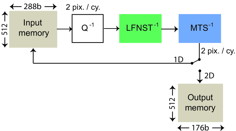
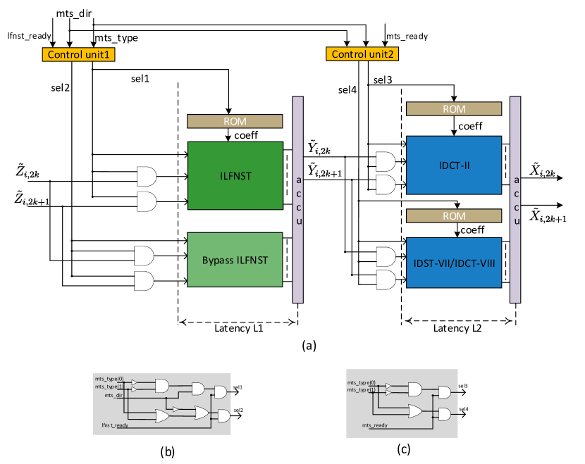
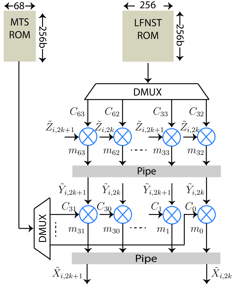
Fig. 6 illustrates the proposed hardware architecture for inverse MTS and LFNST modules. The first control unit, shown in Fig. 6:(b), outputs two selection signals sel1 and sel2 which are derived based on the transform type mts_type (ie. DCT-VII or DCT-VIII/DST-VII) and the direction mts_dir (ie. vertical or horizontal). If the transform type (mts_type) refers to DCT-II, the input samples are processed by the inverse LFNST module, otherwise they go through the Bypass module. The inverse LFNST module uses 32 multipliers in a shared architecture for all block sizes and kernels. Both inverse LFNST and bypass modules have the same latency L1, for that, the Bypass module uses registers to create a delay line with latency L1. At the end of the inverse LFNST, the output samples are accumulated and delivered to the MTS modules in a 2 samples/cycle rate. The second control unit, shown in Fig. 6:(c), delivers two signals sel3 and sel4. These signals are derived from the transform type mts_type. sel3 enables the DCT-II module, while sel4 enables DCT-VIII/DST-VII module. These two modules share 32 multipliers and have the same latency L2. At the end of the transformation, a couple of output samples are delivered through and signals every clock cycle .
IV-A Hardware Separable transform module
The MTS hardware architecture was built based on a constraint of 2 samples/cycle throughput and a fixed latency. The architecture of 4/8/16/32-point DCT-II/VIII, DST-VII and 64-point DCT-II uses 32 Regular Multiplier (RM). Thirty-two is the minimum number of multipliers needed to get a throughput of 2 samples/cycle. This number is bounded by the odd butterfly decomposition of the DCT-II transform matrix and the DCT-VIII/DST-VII transform matrices.
The zeroing concept in VVC applied on large block sizes enable processing one sample/cycle at the input to get a 2 sample/cycle at the output. In fact, for 64-point IDCT, the size of the input vector is 32 and the output vector size is 64. Concerning the 32-point IDCT-VIII/IDST-VII, the size of the input and output vectors are 16 and 32, respectively. In both cases, the output vector is twice the size of the input vector enabling to lower the input rate to one sample per cycle.
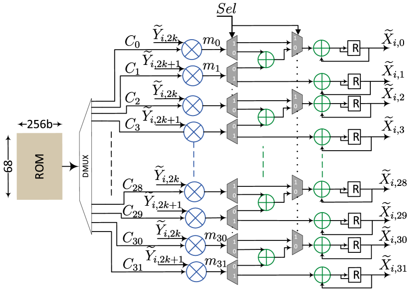
Fig. 7 shows the architecture of the hardware module using 32 RMs referred to . and are the input samples at clock cycle . Using the zeroing for large block sizes, and carry the same input sample. Otherwise, they carry two different samples. The input samples are then multiplied by the corresponding transform coefficients vector , where holds a line of the transform matrix in case of zeroing and two lines otherwise. The output results are then accumulated in the output vector . This accumulation is depicted in the figure through the adders and the feedback lines.
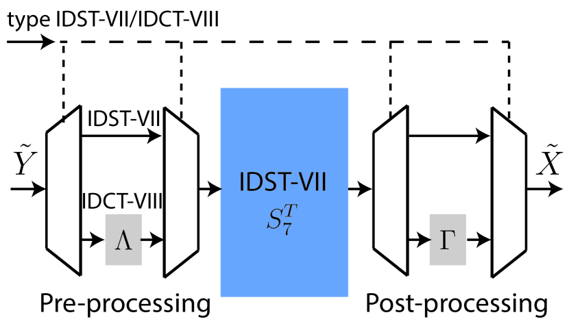
The transform coefficients are stored in a Read-Only Memory (ROM). The total memory size is 17408-bits which corresponds to 68 columns of 256 bit-depth (25668). The ROM stores the coefficients of the 64-point DCT-II, 32-point, 16-point, 8-point and 4-point DST-VII matrix coefficients. The 64-point DCT-II is decomposed using its butterfly structure, and the resultant sub-matrices are stored. Moreover, one sub-matrix (16-point) is replicated in order to respect the output rate. It is well known that IDCT-VIII can be computed from the IDST-VII using pre-processing and post-processing matrices as expressed in (11) [35].
| (11) |
where and are permutation and sign changes matrices computed in (12) and (13), respectively.
| (12) |
| (13) |
with and .
This relationship between DCT-VIII and DST-VII enables to compute both transforms using one kernel. Therefore, we store only the DST-VII transform matrices. Fig. 8 illustrates the unified design to process both DST-VII and DST-VIII. The post and pre-processing matrices do not require any additional multiplication since they are composed of only and involving sign changes and permutation operations.
IV-B Hardware Non-Separable transform module
The non-separable transform or the LFNST was designed on the measure of the 2 samples/cycle throughput. The LFNST architecture supports all VVC transform block sizes including asymmetrical blocks. As discussed in Section II-B, the LFNST operates on the top-left corner of the input block. However, depending on the input block width and height, the 16 residuals of the corner may not all be used. For example, for the 44 block only 8 residuals of the 16 are transformed. The output of the LFNST depends on the input block width and height, which can be either 16 or 48. The 44 top-left corner is zigzag scanned and transformed into a line vector. This latter is then fed to the LFNST module. Table IV presents the input/output sizes of the LFNST core according to the transform block size.
| Block size | Input size | Output size |
| 8 | 16 | |
| 8 | 48 | |
| and () | 16 | 16 |
| and () | 16 | 48 |
We can notice from Table IV that due to the difference between the input and output sizes, their corresponding throughput can also be different. To perform constant throughout for the 44 block, we can lower the input rate to 1 sample per 2 clock cycles. For 88 block sizes, we can lower it to 1 sample per 3 clock cycles. For and blocks, the input rate is set to 2 samples per 3 cycles. Concerning the and () blocks, the input/output rates remain the same, 2 samples/cycle. In all cases, we get the desired output rate of 2 samples/cycle. More details in input/output rates are given in Table V for different block sizes.
| Block size | Input rate | Output rate |
| (sample/cycle) | (sample/cycle) | |
| 1 | 2 | |
| 1/3 | 2 | |
| and () | 2 | 2 |
| and () | 2/3 | 2 |
To perform the secondary transform, LFNST uses a total of 16 kernels, 8 kernels of size and 8 others of size . These kernels are stored in a ROM. The total ROM size is 65536-bits, which corresponds to 256 columns of 256-bits in depth (). Like the MTS, the proposed LFNST design uses 32 RM, which is the minimum number of multipliers needed to satisfy the target 2 samples/cycle rate. As a result, the LFNST core design follows the same design as the MTS depicted in Fig. 7, but unlike the MTS, LFNST adds a delay line at the output.
Fig. 9 depicts the VVC transform (MTS + LFNST) unified design. The proposed designs use in total 64 RM , 32 for the MTS and 32 for the LFNST . As we can see in the Fig. 9, the LFNST is performed before the MTS, from its ROM it retrieves, depending on the LFNST index and set index, the 32 coefficients that correspond to the input residuals shown as with . These coefficients are then fed to the core multipliers along with the input samples and where is the clock cycle. The result of the multiplication is forwarded to the delay line which is depicted by the pipe in the figure. This latter ensures a constant system latency for the LFNST. At the end of the LFNST processing, the output samples feed the MTS module with a rate of 2 samples/cycle through and signals. These samples are then fed to the core multipliers along with the corresponding coefficients retrieved from the MTS ROM with . The final result goes to the second delay line which unifies the latency for the MTS. Finally, the transformed samples are redirected to either the transpose or output memory via and signals. They are directed to the transpose memory if the first direction is selected for the MTS and to the output memory otherwise.
The LFNST + MTS processor control interface is summarized in Table VI. A positive pulse in launches the transform process, with the block size defined by trwidth and trheight. The MTS and LFNST control signals are defined in the interface with prefix and , respectively. For example, the transform type and direction for the MTS are defined in the MTStype and MTSdir input signals, respectively. Following the inputenable the signal will carry two samples at the next clock cycle. These samples are then fed to the LFNST module. The result, carried by LFNSTout, is then sent to the MTS module, which will perform a 2 dimensional transform. After finishing the 2-D transform, the MTS communicates the transformed samples to the output memory via MTSoutfin signal. However, if the first direction is selected for the MTS, the results will be directed to the input memory via MTSoutinter. For both modules that integrate data loading and pipeline stages, the design starts generating the results of the LFNST/1-D MTS after a fixed system latency. It then generates thanks to the piplined architecture the outputs every clock cycle without any stall.
| Signals | I/O | #BITS | Description |
| I | 1 | System Clock | |
| rstn | I | 1 | System reset, active low |
| inputenable | I | 1 | Activation pulse to start |
| AVCVVC | I | 1 | Video standard: 0, AVC; 1, HEVC or VVC |
| trwidth | I | 3 | Transform Block width: 000:4 - 100:64 |
| trheight | I | 3 | Transform Block height: 000:4 - 100:64 |
| MTStype | I | 2 | Tran. type: DCT-II, DCT-VIII and DST-VII |
| MTSdir | I | 1 | Transform direction : 0: Hori.; 1: Vert. |
| LFNSTposx | I | 5 | Position x of vector input |
| LFNSTposy | I | 3 | Position y of vector input |
| LFNSTsetidx | I | 2 | LFNST kernel set index |
| LFNSTidx | I | 2 | LFNST kernel index |
| trsrcin | I | 2 | LFNST input data |
| MTSready | O | 1 | Ready pulse, end of N-point MTS |
| LFNSTready | O | 1 | Ready pulse, end of LFNST |
| MTSoutinter | O | 2 | Intermediate output, 1-D MTS |
| MTSoutfin | O | 2 | Final output, 2-D MTS |
| LFNSTout | O | 2 | LFNST output data |
| Disabled tool | All Intra Main 10 | Random Access Main 10 | Low Delay B Main 10 | ||||||||||||
| Y | U | V | EncT | DecT | Y | U | V | EncT | DecT | Y | U | V | EncT | DecT | |
| MTS | |||||||||||||||
| LFNST | |||||||||||||||
V Experimental Results
V-A Experimental Setup
VHDL hardware description language is used to describe the proposed transform block. A state-of-the-art logic simulator [38] is used to test the functionality of the VVC transform module (MTS + LFNST). The design was synthesised by a commercial Design Compiler using 28-nm technology. The test strategy is performed as follows. First a set of pseudo-random input vectors have been generated and used as test patterns to test the 1-D MTS in unit tests. The same number of tests was used to verify the LFNST module. Second, a software implementation of the inverse MTS and LFNST has been developed, based on the transform procedures defined in the Versatile Video Coding Test Model (VTM) version 8.0 [39]. Using self-check technique, the bit accurate test-bench compares the simulation results with those obtained using the reference software implementation. The tests cover all transform block sizes from to including asymmetric blocks, for both MTS and LFNST modules.
V-B Results and Analysis
V-B1 Coding performance
First the coding gain and software complexity of the MTS and LFNST modules under the VVC common Test Conditions in three main coding configurations including All Intra, Random Access and Low Delay B are analysed [40]. Table VII [36] gives the coding losses and the complexity reductions at both encoder and decoder when the MTS and LFNST tools are turned off. We can notice that disabling MTS and LFNST tools introduces the highest coding losses in All Intra coding configuration with 1.32% and 0.99% BD-BR [41, 42] losses when these two tools are disabled, respectively. The MTS and LFNST tools are active only for Intra blocks to limit the complexity overhead at the encoder side. This may explain the higher coding gain brought by the MTS and LFNST in All Intra configuration compared to the two other Inter configurations. Moreover, the MTS tool significantly increases the encoder complexity since five sets of horizontal and vertical transforms are tested to select the best performing set of transforms in terms of rate distortion cost. At the decoder side, the MTS slightly increases the decoder complexity since only one transform set is processed by block. This slight complexity overhead is mainly caused by introducing more complex transforms including DST-VII, DCT-VIII and DCT-II of size 64. Disabling the LFNST tool changes the encoder behaviour resulting in complexity increase at the encoder side caused by complexity reduction tools included in the VTM to speedup the encoder such as early termination [43, 44]. In fact, the LFNST tool enables more efficient coding of residuals resulting in better energy packing and more coefficients are set to zeros after the quantisation. Therefore, the early termination techniques integrated in the VTM [43] terminate the RDO process earlier when the LFNST is enabled resulting in lower encoding time. At the decoder side, disabling the LFNST slightly decreases the decoder complexity since LFNST is applied only on blocks processed by the DCT-II primary transform. We can conclude from this study that both MTS and LFNST have a slight impact on the software decoder complexity. In the next section, the impact of both MTS and LFNST tools will be investigated on a hardware decoder targeting an ASIC platform.
V-B2 MTS performance
The proposed 1-d MTS design was synthesized using Design Compiler (DC) targeting an 28-nm ASIC at 600 MHz. The design sustain 2 samples/cycle with a fixed system latency. The total area consumed by the 1-D MTS is 87.7 Kgates. The 2-D MTS is applied using the 1-D core in a folded architecture, where the output of the first direction is redirected to a transpose memory which re-sends the transposed data to the same 1-D core. As a result the 2-D MTS includes both 1-D MTS and the transpose memory. The same architecture can be found in many state of the art works, however the proposed MTS design supports all sizes and types of VVC transform including the block of order 64 for the DCT-II. This design proved to be scalable enabling to doubled the performance of the design from a throughput of 2 samples/cycle to a throughput of 4 samples/cycle. The flexibility of the design allowed this transition to be done only by doubling the total number of multipliers from 32 to 64 multipliers while conserving the same architecture. Table VIII shows the synthesis results for both design, the 4 samples/cycle design increases the area cost by 55% instead of 100% and this is because doubling the number of multipliers reduces the size of the delay line which is not negligible compared to the total area size.
| MTS-2p/c | MTS-4p/c | ||
| ASIC 28-nm | Num. of mult. | 32 | 64 |
| Combinational area | 59135 | 97210 | |
| Non-combinational area | 29946 | 41705 | |
| Total area (gate count) | 89082 | 138916 |
| LFNST-2p/c | LFNST-4p/c | ||
| ASIC 28-nm | Num. of mult. | 32 | 64 |
| Combinational area | 49911 | 79409 | |
| Noncombinational area | 24680 | 29806 | |
| Total area (gate count) | 74592 | 109215 |
| VVC | HEVC | ||
| ASIC 28-nm | Architecture | RM | MCM |
| Total area | 163672 | 41500 |
| Solutions | Garrido et al. [31] | Proposed architecture |
| Technology | ME 20 nm FPGA | Arria 10 FPGA |
| ALMs | 5179 | 9723 |
| Registers | 9104 | 14368 |
| DSPs | 32 | 32 |
| Frequency (MHz) | 204 | 165 |
| Throughput (fps) | 1920 1080p40 | 19201080p50 |
| Memory | 3910Kb | |
| MTS size | 4, 8, 16, 32, 64 | 4, 8, 16, 32, 64 |
| MTS type | DCT-II/VIII, DST-VII | DCT-II/VIII, DST-VII |
| Solutions | Jia et al. [23] | Mert et al. [26] | Fan et al. [32] | Proposed architecture |
| Technology | ASIC 90 nm | ASIC 90 nm | ASIC 65 nm | ASIC 28 nm |
| Gates | 235400 | 417000 | 496400 | 163674 |
| Frequency (MHz) | 311 | 160 | 250 | 600 |
| Throughput (fps) | 1920 1080p20 | 7680 4320p39 | 38402160p30 | |
| Memory | Kb | Kb | ||
| MTS size | 4, 8, 16, 32 | 4, 8 | 4, 8, 16, 32 | 4, 8, 16, 32, 64 |
| MTS type | DCT-II, Hadamard | DCT-II/VIII, DST-VII | DCT-VIII, DST-VII | DCT-II/VIII, DST-VII |
| LFNST | ✗ | ✗ | ✗ | ✓ |
| LFNST size | to |
V-B3 LFNST performance
Like the MTS the proposed LFNST design was synthesized using Design Compiler (DC) targeting an 28-nm ASIC at 600 MHz. Because it is chained to the 1-D MTS it sustains the same throughput of 2 samples/cycle with a fixed system latency. The total area consumed by the LFNST design is 71.6 Kgates. Unlike the MTS, the LFNST is a new tool introduced in the VVC standard. That is why no study was found in literature that investigates a hardware implementation of LFNST. As a result, this work is the first study for a hardware architecture for the LFNST. Similar to MTS, the scalability of LFNST design enabled a very flexible transition going from a throughput of 2 samples/cycle to a throughput of 4 samples/cycle. The design proved to be scalable, doubling the throughput comes only at the expense of doubling the total number of multipliers while the same architecture is preserved. Table IX shows the synthesis results for both designs, the 4 samples/cycle design increases the area cost by 46.5% instead of doubling it and this is because the delay line is reduced. We notice that the percentage of area increase for the LFNST is lower than for the MTS. This caused by the delay line of the LFNST which is larger than in the MTS.
V-B4 VVC Transform vs HEVC Transform
To compare the VVC transform and the HEVC transform, we synthesised two 1-D design that are similar in throughput. The 1-D HEVC transform supports all DCT-II and DST for block size , it has a throughput of 2 samples/cycle with a static system latency. The VVC transform supports all MTS types and sizes and all LFNST sizes with a throughput of 2 samples/cycle and a fixed system latency. The difference between the two transforms is that the VVC one is designed based on a RM architecture while HEVC transform is designed using a Multiple Constant Multiplier (MCM) based architecture. Many study proved that using MCM based architecture for HEVC transform is more efficient in terms of area than using RM based one. However, based on our previous study in [14], it turns out that for VVC using RM based architecture is more area efficient due to the new transform types and sizes. This fact proves that both architectures are optimally designed and thus giving more credibility for fair comparison. Table X shows the performance results of both designs. We can notice that the area of VVC transform is 4 time larger than the HEVC transform block, this is considered to be reasonable rather good due of the new tools and new sizes introduced in VVC.
V-B5 Hardware synthesis performance
The proposed design supports the transform block of three different video standards including AVC/H.264, HEVC/H.265 and the emerging VVC/H.266 standard. The 1-D MTS core operates at 600 MHz with a total of 89K cell area and 17408-bits of ROM used to store MTS kernels. The LFNST core operates at 600 MHz with a total of 74.5K cell area and 32768-bits of ROM used to store its kernels. Integrating these modules together adds two memories one for the transform coefficients (input) and the other for transformed samples (output). The input and output memories are SRAMs that can hold a CTU of size for 4:2:2 chroma subsampling. The Input memory is used as transpose memory for the 2-D MTS. It stores one Luma CTB of size and two Chroma CTBs of size . The input sample size is 18-bits which makes the total input memory size 147456-bits. The output sample size is 11-bits resulting in a total of 90112-bits for the output memory.
A fair comparison with the state of the art solutions is quite difficult since most of works focus on earlier versions of the VVC MTS and do not support the LFNST. Table XI and XII give the key performance of state-of-the-art FPGA and ASIC-based works, respectively. The only work that supports all MTS types and sizes is found in [31] and its performance is presented in Table XI for FPGA platform. Compared to our MTS design on FPGA platform, we consume more resources in terms of Adaptive Logic Modules (ALMs) and registers, but on the other hand, we do not use any additional memory. Both designs support the complete version of VVC MTS with similar performance, however, in this paper we add the LFNST tool which requires nearly the same hardware resource as the MTS module.
The solutions proposed in [23, 26, 32] support only the MTS module on ASIC platform. Gate count is the logical calculation part and it can be seen from Table XII that compared with implementations of Jia et al. [23], Mert et al. [26] and Fan et al. [32], our solution has several advantages. We present a unified transform architecture that can process inverse MTS and LFNST supporting all kernel sizes including asymmetric sizes and all types (Inverse DCT (IDCT)-II/VIII and Inverse DST (IDST)-VII) in the two dimensions. Although our design supports more transform types and sizes than [23], we still reduce the total area by up to 44% and that’s due to our multiplications design relying on shared regular multipliers. Compared to [26] and [32], our design requires 3 times less area.
VI Conclusion
In this paper a hardware implementation of the inverse VVC transform module has been investigated targeting a real time VVC decoder on ASIC platforms. The VVC transform module consists of a primary transform block and a secondary transform block called MTS and LFNST, respectively. The proposed hardware implementation relies on regular multipliers and sustains a constant system latency with a fixed throughput of 1 cycle per sample. The MTS design leverage all primary transform optimisations including butterfly decomposition for DCT-II, zeroing for 64-point DCT-2 and 32-point DST-VII/DCT-VIII, and the linear relation between DST-VII and DCT-VIII. The proposed design uses 64 regular multipliers (32 for MTS and 32 for LFNST) enabling to reach real time decoding of 4K video (4:2:2) at 30 frames par second. This architecture is scalabale and can easily be extended to reach a higher frame rate of 60 frames per second by using 128 regular multipliers.
The proposed transform design has been successfully integrated in a hardware ASIC decoder supporting the transform module of recent MPEG standards including AVC, HEVC and VVC. The hardware ASIC decoder will be integrated in consumer devices to decode AVC, HEVC and VVC videos.
References
- [1] B. Bross, J. Chen, J.-R. Ohm, G. J. Sullivan, and Y.-K. Wang, “Developments in international video coding standardization after avc, with an overview of versatile video coding (vvc),” Proceedings of the IEEE, pp. 1–31, 2021.
- [2] W. Hamidouche, T. Biatek, M. Abdoli, E. François, F. Pescador, M. Radosavljević, D. Menard, and M. Raulet, “Versatile video coding standard: A review from coding tools to consumers deployment,” arXiv preprint arXiv:2106.14245, 2021.
- [3] F. Bossen, X. Li, A. Norkin, and K. Sühring, “Jvet-o0003.” JVET AHG report: Test model software development (AHG3), July. 2019.
- [4] N. Sidaty, W. Hamidouche, P. Philippe, J. Fournier, and O. Déforges, “Compression Performance of the Versatile Video Coding: HD and UHD Visual Quality Monitoring.” Picture Coding Symposium (PCS), November 2019.
- [5] X. Zhao, S.-H. Kim, Y. Zhao, H. E. Egilmez, M. Koo, S. Liu, J. Lainema, and M. Karczewicz, “Transform coding in the vvc standard,” IEEE Transactions on Circuits and Systems for Video Technology, pp. 1–1, 2021.
- [6] G. Plonka and M. Tasche, “Fast and Numerically Stable Algorithms for Discrete Cosine Transforms,” Linear Algebra and its Applications, vol. 394, pp. 309 – 345, 2005.
- [7] C. Loeffler, A. Ligtenberg, and G. S. Moschytz, “Practical fast 1-D DCT algorithms with 11 multiplications,” in International Conference on Acoustics, Speech, and Signal Processing (ICASSP), vol. 2, May 1989, pp. 988 – 991.
- [8] M. Vetterli and H. J. Nussbaumer, “Simple FFT and DCT algorithms with reduced number of operations,” IEEE Journal on Signal Processing, vol. 6, no. 4, pp. 267 – 278, 1984.
- [9] R. K. Chivukula and Y. A. Reznik, “Fast Computing of Discrete Cosine and Sine Transforms of Types VI and VII,” in Proc. SPIE, vol. 8135, 2011, pp. 8135 – 8135 – 10.
- [10] M. Puschel and J. M. F. Moura, “Algebraic Signal Processing Theory: Cooley-Tukey Type Algorithms for DCTs and DSTs,” IEEE Transactions on Signal Processing, vol. 56, no. 4, pp. 1502 – 1521, April 2008.
- [11] Z. Zhang, X. Zhao, X. Li, Z. Li, and S. Liu, “Fast Adaptive Multiple Transform for Versatile Video Coding,” in Data Compression Conference (DCC), 2019.
- [12] P. Meher, S. Park, B. Mohanty, K. Lim, and C. Yeo, “Efficient integer dct architectures for hevc,” IEEE Transactions on Circuits and Systems for Video Technology, vol. 24, no. 1, pp. 168–178, Jan 2014.
- [13] W. Park, B. Lee, and M. Kim, “Fast computation of integer dct-v, dct-viii and dst-vii for video coding,” IEEE Transactions on Image Processing, pp. 1–1, 2019.
- [14] I. Farhat, W. Hamidouche, A. Grill, D. Menard, and O. Déforges, “Lightweight hardware implementation of vvc transform block for asic decoder,” in ICASSP 2020 - 2020 IEEE International Conference on Acoustics, Speech and Signal Processing (ICASSP), 2020, pp. 1663–1667.
- [15] A. Saxena and F. C. Fernandes, “DCT/DST-Based Transform Coding for Intra Prediction in Image/Video Coding,” IEEE Transactions on Image Processing, vol. 22, no. 10, pp. 3974–3981, Oct 2013.
- [16] A. Arrufat, P. Philippe, K. Reuzé, and O. Déforges, “Low complexity transform competition for hevc,” in 2016 IEEE International Conference on Acoustics, Speech and Signal Processing (ICASSP), March 2016, pp. 1461–1465.
- [17] T. Biatek, V. Lorcy, and P. Philippe, “Transform competition for temporal prediction in video coding,” IEEE Transactions on Circuits and Systems for Video Technology, pp. 1–1, 2018.
- [18] X. Zhao, J. Chen, M. Karczewicz, A. Said, and V. Seregin, “Joint Separable and Non-Separable Transforms for Next-Generation Video Coding,” IEEE Transactions on Image Processing, vol. 27, no. 5, pp. 2514–2525, May 2018.
- [19] X. Zhao, J. Chen, A. Said, V. Seregin, H. E. Egilmez, and M. Karczewicz, “Nsst: Non-separable secondary transforms for next generation video coding,” in 2016 Picture Coding Symposium (PCS), 2016, pp. 1–5.
- [20] M. Koo, M. Salehifar, J. Lim, and S.-H. K. and, “Low Frequency Non-Separable Transform (LFNST),” in Picture Coding Symposium (PCS), November 2019.
- [21] T. Wiegand, G. J. Sullivan, G. Bjontegaard, and A. Luthra, “Overview of the h.264/avc video coding standard,” IEEE Transactions on Circuits and Systems for Video Technology, vol. 13, no. 7, pp. 560–576, 2003.
- [22] S. Shen, W. Shen, Y. Fan, and X. Zeng, “A Unified 4/8/16/32-Point Integer IDCT Architecture for Multiple Video Coding Standards,” in 2012 IEEE International Conference on Multimedia and Expo, July 2012, pp. 788–793.
- [23] J. Zhu, Z. Liu, and D. Wang, “Fully pipelined dct/idct/hadamard unified transform architecture for hevc codec,” in 2013 IEEE International Symposium on Circuits and Systems (ISCAS2013), May 2013, pp. 677–680.
- [24] M.Chen, Y. Zhang, and C. Lu, “Efficient architecture of variable size HEVC 2D-DCT for FPGA platforms,” Int. J. of Electronics and Communications, vol. 73, pp. 1–8, March 2017.
- [25] A. Ahmed and M. Shahid, “N Point DCT VLSI Architecture for Emerging HEVC Standard,” VLSI Design, pp. 1–13, 2012.
- [26] A. Mert, E. Kalali, and I. Hamzaoglu, “High Performance 2D Transform Hardware for Future Video Coding,” IEEE Transactions on Consumer Electronics, vol. 62, no. 2, May 2017.
- [27] M. Garrido, F. Pescador, M. Chavarrias, P. Lobo, and C. Sanz, “A High Performance FPGA-based Architecture for Future Video Coding Adaptive Multiple Core Transform,” IEEE Transactions on Consumer Electronics, March 2018.
- [28] M. J. Garrido, F. Pescador, M. ChavarrÃas, P. J. Lobo, and C. Sanz, “A 2-d multiple transform processor for the versatile video coding standard,” IEEE Transactions on Consumer Electronics, vol. 65, no. 3, pp. 274–283, Aug 2019.
- [29] A. Kammoun, S. B. Jdidia, F. Belghith, W. Hamidouche, J. F. Nezan, and N. Masmoudi, “An optimized hardware implementation of 4-point adaptive multiple transform design for post-HEVC,” in 2018 4th International Conference on Advanced Technologies for Signal and Image Processing (ATSIP), March 2018, pp. 1–6.
- [30] A. Kammoun, W. Hamidouche, F. Belghith, J. Nezan, and N. Masmoudi, “Hardware Design and Implementation of Adaptive Multiple Transforms for the Versatile Video Coding Standard,” IEEE Transactions on Consumer Electronics, vol. 64, no. 4, October 2018.
- [31] M. J. Garrido, F. Pescador, M. Chavarrías, P. J. Lobo, C. Sanz, and P. Paz, “An fpga-based architecture for the versatile video coding multiple transform selection core,” IEEE Access, vol. 8, pp. 81 887–81 903, 2020.
- [32] Y. Fan, Y. Zeng, H. Sun, J. Katto, and X. Zeng, “A pipelined 2d transform architecture supporting mixed block sizes for the vvc standard,” IEEE Transactions on Circuits and Systems for Video Technology, pp. 1–1, 2019.
- [33] Intel-FPGA-Integer-Arithmetic-IP-Cores-User-Guide, “Intel 2017,” [Onine]_ Available: https://www.altera.com/en-US/pdfs/literature/ug/ug-lpm-alt-mfug.pdf.
- [34] A. Kammoun, W. Hamidouche, P. Philippe, O. Déforges, F. Belghith, N. Masmoudi, and J. Nezan, “Forward-inverse 2d hardware implementation of approximate transform core for the vvc standard,” IEEE Transactions on Circuits and Systems for Video Technology, pp. 1–1, 2019.
- [35] Y. A. Reznik, “Relationship between DCT-II, DCT-VI, and DST-VII transforms,” in 2013 IEEE International Conference on Acoustics, Speech and Signal Processing, May 2013, pp. 5642–5646.
- [36] W.-J. Chien and J. Boyce, “Jvet ahg report: Tool reporting procedure (ahg13).” JVET document R0013, 18th Meeting: by teleconference, April 2020.
- [37] X. L. K. Sühring, “Jvet common test conditions and software reference configurations.” JVET Document JVET-H1010, November 2017.
- [38] (2018) RivieraPro-Aldec-Functional-Verification-Tool. [Online]:https://www.aldec.com/en/products/functional_verification/riviera-pro.
- [39] J. Chen, Y. Ye, and S. H. Kim, “Algorithm description for versatile video coding and test model 8 (vtm 8).” JVET AHG report: Test model software development (AHG3), January 2020.
- [40] F. Bossen, J. Boyce, K. Suehring, X. Li, and V. Seregin, “JVET common test conditions and software reference configurations for SDR video,” in JVET document K1010 (JVET-K1010), July 2018.
- [41] G. Bjøntegaard, “Calcuation of Average PSNR Differences Between RD-curves,” in VCEG-M33 ITU-T Q6/16, Austin, TX, USA, 2-4 April, 2001.
- [42] G. Bjøntegaard, “Improvements of the BD-PSNR model,” ITU-T SG16 Q, vol. 6, p. 35, 2008.
- [43] A. Wieckowski, J. Ma, H. Schwarz, D. Marpe, and T. Wiegand, “Fast partitioning decision strategies for the upcoming versatile video coding (vvc) standard,” in 2019 IEEE International Conference on Image Processing (ICIP), 2019, pp. 4130–4134.
- [44] T. Amestoy, A. Mercat, W. Hamidouche, D. Menard, and C. Bergeron, “Tunable vvc frame partitioning based on lightweight machine learning,” IEEE Transactions on Image Processing, vol. 29, pp. 1313–1328, 2020.
![[Uncaptioned image]](/html/2107.11659/assets/Figures/IbrahimFarhat-bw.jpg) |
Ibrahim Farhat was born in Eljem, Tunisia, in 1993. He received the engineering degree in communication systems and computer science from SUP’COM school of engineering, Tunis, in 2018. In 2019, he joined the Institute of Electronic and Telecommunication of Rennes (IETR), Rennes, and became a member of VITEC company hardware team, France, where he is currently pursuing the Ph.D. degree. His research interests focus on video coding, efficient real time and parallel architectures for the new generation video coding standards, and ASIC/FPGA hardware implementations. |
![[Uncaptioned image]](/html/2107.11659/assets/Figures/wassim_hamidouche.jpg) |
Wassim Hamidouche received Master’s and Ph.D. degrees both in Image Processing from the University of Poitiers (France) in 2007 and 2010, respectively. From 2011 to 2013, he was a junior scientist in the video coding team of Canon Research Center in Rennes (France). He was a post-doctoral researcher from Apr. 2013 to Aug. 2015 with VAADER team of IETR where he worked under collaborative project on HEVC video standardisation. Since Sept. 2015 he is an Associate Professor at INSA Rennes and a member of the VAADER team of IETR Lab. He has joined the Advanced Media Content Lab of bcom IRT Research Institute as an academic member in Sept. 2017. His research interests focus on video coding and multimedia security. He is the author/coauthor of more than one hundred and forty papers at journals and conferences in image processing, two MPEG standards, three patents, several MPEG contributions, public datasets and open source software projects. |
![[Uncaptioned image]](/html/2107.11659/assets/Figures/Photo_AGR-bw.jpg) |
Adrien Grill was born in 1988 in Aix-en-Provence, France. After receiving his engineering degree at Supelec in 2010, he specialized in hardware algorithm implementation. He joined Vitec in 2014, and currently works as technical leader on codec implementation projects. His fields of interest include signal, image processing, and video coding. |
![[Uncaptioned image]](/html/2107.11659/assets/Photo-Daniel-Menard.jpg) |
Daniel Ménard received the Ph.D. and Habilitation degrees in Signal Processing and Telecommunications from the University of Rennes, respectively in 2002 and 2011. Since 2012, he has been Full-Professor at INSA Rennes - department of Electrical and Computer Engineering and member of the IETR lab. He has 20 years of expertise in the design and implementation of image and signal processing systems. His research interests include low power video codecs, approximate computing and energy consumption. He has a long experience of collaborative projects, he has been involved in different national and European projects He is currently member of different Technical Program Committees of international conferences (ICASSP, SiPS and DATE). Since 2018, he has been an elected member of the Technical Committee ASPS of the IEEE Signal Processing society. He has published more than 100 scientific papers in international journal and conferences. |
![[Uncaptioned image]](/html/2107.11659/assets/Olivier_Deforges.jpg) |
Olivier Déforges received the Ph.D. degree in image processing in 1995. He is a Professor with the National Institute of Applied Sciences (INSA) of Rennes. In 1996, he joined the Department of Electronic Engineering, INSA of Rennes, Scientic and Technical University. He is a member of the Institute of Electronics and Telecommunications of Rennes (IETR), UMR CNRS 6164 and leads the IMAGE Team, IETR Laboratory including 40 researchers. He has authored over 130 technical papers. His principal research interests are image and video lossy and lossless compression, image understanding, fast prototyping, and parallel architectures. He has also been involved in the ISO/MPEG standardization group since 2007. |