High Coherence in a Tileable 3D Integrated Superconducting Circuit Architecture
Abstract
We report high qubit coherence as well as low crosstalk and single-qubit gate errors in a superconducting circuit architecture that promises to be tileable to 2D lattices of qubits. The architecture integrates an inductively shunted cavity enclosure into a design featuring non-galvanic out-of-plane control wiring and qubits and resonators fabricated on opposing sides of a substrate. The proof-of-principle device features four uncoupled transmon qubits and exhibits average energy relaxation times , pure echoed dephasing times , and single-qubit gate fidelities as measured by simultaneous randomized benchmarking. The 3D integrated nature of the control wiring means that qubits will remain addressable as the architecture is tiled to form larger qubit lattices. Band structure simulations are used to predict that the tiled enclosure will still provide a clean electromagnetic environment to enclosed qubits at arbitrary scale.
I Introduction
Building 2D lattices of hundreds or thousands of individually addressable, highly coherent qubits is an outstanding hardware challenge. Anticipated applications include demonstrations of logical gates using the surface code [1, 2, 3, 4] and quantum simulations of 2D lattice Hamiltonians [5, 6]. Superconducting circuits are a promising platform for realizing such lattices [6, 7, 8]; qubits are lithographically defined on 2D substrates, and tailored coupling circuitry can be included in the regions between qubits to realize a universal gate set. Two requirements for scaling such superconducting qubit lattices are: (1) a method to route control wiring to the circuit such that all qubits remain addressable and measurable at progressively larger scales; and (2) a means of preventing low frequency spurious modes from emerging in the circuit as the dimensions increase [9]. These modes can arise from sections of spurious planar transmission lines such as slotlines [10, 11], or from 3D cavity enclosures that house the circuit [11]. Solutions to these scaling challenges must not introduce significant decoherence channels to qubits; and if fault tolerance is desired, must be compatible with gate fidelities beyond the thresholds of quantum error correction codes.
To overcome the wiring limitations of edge-connected circuits, 3D integrated control wiring is a practical solution. Various approaches to this have been demonstrated, for example with spring-loaded pogo pins [12, 13] and with galvanic bonding of the qubit substrate to a wiring/interposer substrate [14, 15, 16]. To avoid spurious modes due to slotlines, divided ground planes can be inductively shunted with airbridges [10] or with superconducting through substrate vias (TSVs) [17, 15, 18]. To avoid low frequency cavity modes, one solution is to divide the quantum processor into subsystems, with each subsystem enclosed in a cavity with dimensions [19, 20, 21, 22]. Alternatively, circuits can be enclosed in inductively shunted cavities that can scale arbitrarily in two dimensions with a cutoff frequency to cavity modes [23, 24].
In this work, we present experimental results on a four-qubit proof-of-principle circuit incorporating this latter concept. The circuit architecture, based on that introduced in Refs. [25, 26], features 3D integrated out-of-plane control wiring and qubits and readout resonators that are fabricated on opposing sides of a substrate. We incorporate a key new feature: inductively shunting the circuit enclosure with a CNC machined pillar that passes through the substrate. This design is established to be compatible with transmon coherence times exceeding , as well as low crosstalk and single-qubit gate errors. Simulations of band structure are used to predict that 2D qubit lattices can be formed by tiling a unit cell within the architecture, without the emergence of low frequency cavity modes and with exponentially decaying cavity mediated crosstalk between qubits.
II Device Architecture
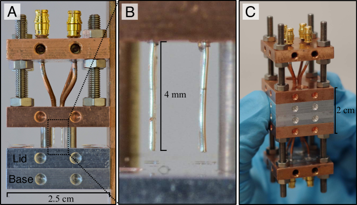
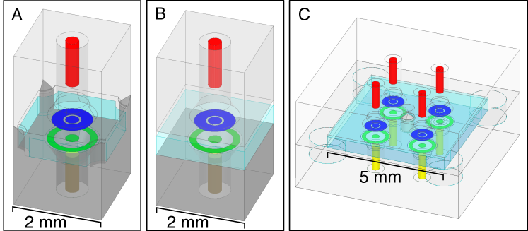
Fig. 1 shows optical images of the cavity enclosure and circuit.
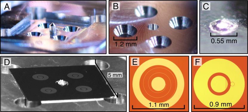
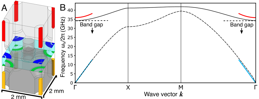
The enclosure base [Fig. 1(A)] features a single central ‘pillar’, and the lid [Fig. 1(B)] contains a matching cylindrical recess that is filled with a ball of indium [Fig. 1(C)]. The base and lid both contain four tapered through-holes that act as waveguides for qubit and resonator control signals. In Fig. 1(D), the circuit substrate is shown placed inside the enclosure base. An aperture has been machined in the center of the substrate allowing the pillar to pass through. The four coaxial transmon [27] qubits are visible, arranged in a lattice with spacing.
Fig. 2 shows a schematic of the out-of-plane wiring design, the inductive shunt design, and the circuit layout. Control signals are routed to qubits and resonators by UT47-type coaxial cables with characteristic impedance . As shown in Fig. 2(A), the inner conductor of each cable, radius , extends a distance into a through-hole in the circuit base/lid part, radius , forming a coaxial waveguide with characteristic impedance . In this device, and (at room temperature) such that when ideally aligned , a close match to the coaxial cable impedance . The PTFE in the coaxial cable is separated from the circuit substrate by approximately , reducing qubit/resonator electric field participation [28] in this lossy dielectric. The inner conductor of the coaxial cable terminates a distance from the qubit/resonator that it addresses. The coupling of control signals to qubits/resonators is dominantly mediated by an evanescent circular waveguide mode [29], with coupling strength , . For , . In this device, for each qubit (resonator) control line. Fig. 2(B) shows a schematic cross-section of the pillar in the enclosure base, passing through the aperture in the circuit substrate and galvanically connecting to the indium filled recess in the enclosure lid. The pillar acts as a ‘bulk via’ that inductively shunts the two halves of the enclosure, without requiring side wall metallization of the substrate aperture or a galvanic connection between the substrate and enclosure. Fig. 2(C) shows the circuit layout. The reverse side of the substrate rests directly on the enclosure base and contains four lumped LC ‘spiral’ resonators. Each resonator is coaxially aligned with and capacitively coupled to a qubit. The cavity enclosure provides the ground, and there are no ground planes on the substrate.
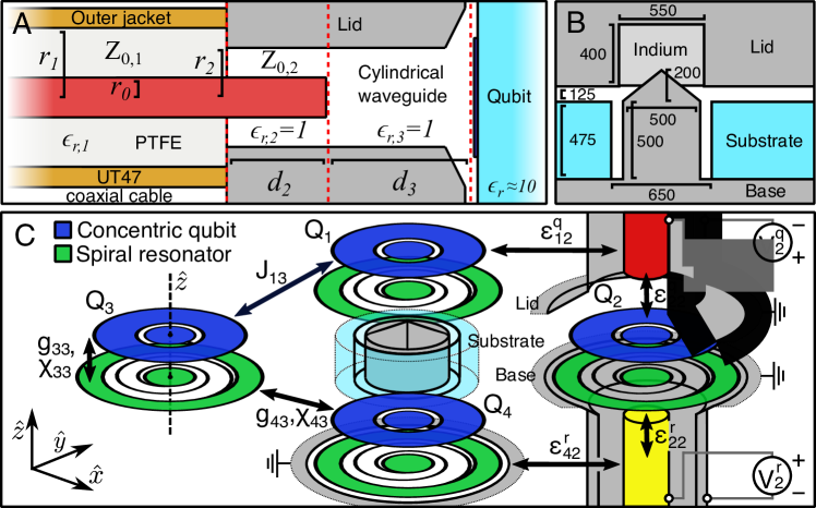
The qubit (resonator) electrodes are electrically floating and are designed to have a shortest distance to the surface of the cavity enclosure of approximately ().
| 3.981 | 7.968 | -199 | 69 | -165 | 124 | 118 | 110 | 13 | |
| 4.045 | 8.083 | -199 | 71 | -167 | 126 | 73 | 75 | 18 | |
| 4.130 | 8.183 | -198 | 74 | -169 | 128 | 749 | 515 | 13 | |
| 4.192 | 8.289 | -197 | 76 | -164 | 128 | 241 | 160 | 10 |
III Basic characterization
An effective dispersive Hamiltonian for the low energy spectrum of the device is given by
| (1) |
Here, () and () are the creation (annihilation) operators for qubit and resonator respectively; is the transition frequency of qubit given zero photons in resonator ; is the anharmonicity of qubit ; is the frequency of resonator given qubit is in its ground state; is the dispersive shift between qubit and resonator ; and () describe the coupling of qubit (resonator) to qubit (resonator) control line , which is driven with a voltage (). These voltages are applied close to the cylindrical waveguide transition and at a fixed distance from the circuit [see Fig. 2(C)]. contains undesired crosstalk terms that are discussed in the crosstalk characterization section.
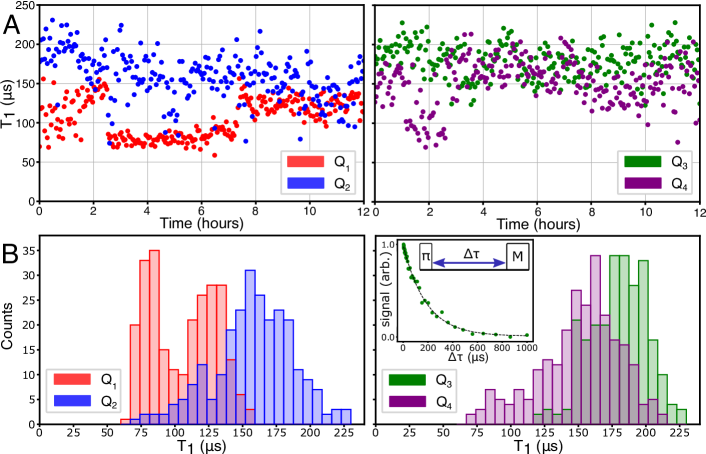
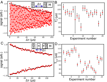
The quantities , , and were determined using standard spectroscopic measurements and Ramsey measurements, and are shown in Table 1. The relaxation times of the four qubits were simultaneously measured repeatedly over a period of 12 hours. The consecutive measured values and resulting histograms are shown in Fig. 3. The characteristic dephasing times and were measured using standard Ramsey and Hahn echo pulse sequences (see Appendices). The coherence times are summarized in Table 2.
| EPG sep | EPG sim | EPG coh lim | |||||
|---|---|---|---|---|---|---|---|
| 106(24) | 95(5) | 101(9) | 193(52) | 2.29(4) | 1.64(4) | 1.1(1) | |
| 159(30) | 104(9) | 116(6) | 183(25) | 1.46(6) | 2.15(8) | 0.94(5) | |
| 179(21) | 89(12) | 128(9) | 199(25) | 1.16(5) | 1.31(5) | 0.85(5) | |
| 151(30) | 99(8) | 113(4) | 181(24) | 2.23(4) | 2.16(4) | 0.97(5) | |
| Avg. | 149(38) | 97(10) | 115(12) | 189(34) | 1.8(5) | 1.8(4) | 1.0(1) |
IV Crosstalk characterization
The device is a proof-of-principle demonstration of the circuit architecture with no intentional couplings except between qubit-resonator pairs; as such, we identify all other couplings as undesired crosstalk. The crosstalk terms that were considered are defined in the following effective Hamiltonian:
| (2) |
Here, is a parasitic transverse coupling between qubits and , satisfying ; is a parasitic dispersive shift between qubit and resonator ; and () describes a parasitic coupling between qubit (resonator) and qubit (resonator) control line . Some examples of these different types of crosstalk are shown pictorially in Fig. 2(C). The following expression was used to relate the dispersive shift to a transverse coupling between transmon qubit and resonator [27]
| (3) |
where and is the charging energy of qubit .
The experimentally bounded maximum parasitic transverse couplings are summarized in Table 3, along with the predicted maximum values found by applying a simple impedance formula [31] to HFSS [32] driven terminal simulations (see Appendices).
IV.1 Qubit control line selectivity
| Crosstalk quantity | Experiment | Simulation |
|---|---|---|
| Qubit-qubit coupling | 10 | |
| Qubit-resonator coupling | 50 |
The qubit control line selectivity is here defined
| (4) |
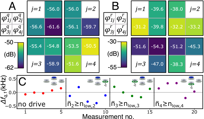
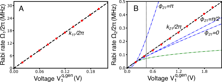
The selectivity was measured by driving qubit at frequency over a range of generator drive voltages and fitting the induced Rabi oscillation rate to the linear function . From the measured linear response in the strong drive regime , it is inferred that , where (see Appendices). In this case, the selectivity takes the simple form . The measured qubit control line selectivities are shown in Fig. 4(A), and the plots of vs. that were used to determine are shown in Fig. A4. Making use of the fact in this device results in the following experimental bound on the transverse coupling : .
IV.2 Resonator control line selectivity
The resonator control line selectivity is here defined
| (5) |
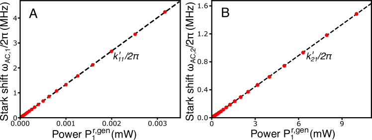
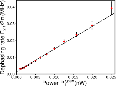
The selectivity was measured by continuously driving resonator at frequency , where ( is the total decay rate of resonator ), over a range of generator drive powers . The induced AC Stark-shift in qubit was then fit to the linear function . The selectivity is then given by (see Appendices). The measured resonator control line selectivities are shown in Fig. 4(B), and the plots of vs. that were used to determine are shown in Fig. A5.
IV.3 Parasitic qubit-resonator coupling
To measure the parasitic dispersive shift between qubit and resonator , resonator was continuously driven at frequency from its own control line to populate it with a steady-state photon number of at least , where is the critical photon number [33] of resonator (see Appendices).
Ramsey experiments were then performed on qubit () to measure the parasitic AC Stark-shift as shown in Fig. 4(C). No AC Stark-shift was detected for any combination of qubit and resonator , with a frequency resolution of approximately , resulting in the approximate bound using the dispersive relation [36].
V Single qubit gate errors
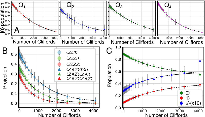
Single qubit randomized benchmarking (RB) [37, 35] was performed on all four qubits both separately and simultaneously, using a combination of duration ( Blackman envelope with buffer) physical gates with DRAG pulse shaping [38], and virtual gates [39]. Single-shot readout was performed for all the RB experiments (see Materials and Methods). Fig. 5(A) shows the fitted RB curves for the simultaneous RB experiment. The RB protocol was run at Clifford sequence lengths and for different sequences of Clifford gates.
Each of the experiments were repeated times to build statistics. The resulting error-per-physical-gates (EPG) are presented in Table 2.
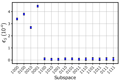
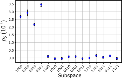
Correlated RB (CorrRB) [34] was performed using the simultaneous RB experiment data. Fig. 5(B) shows a selection of the Pauli- correlators vs. Clifford sequence length . These were fit to standard RB curves , where as defined in Ref. [34]. From the fitted depolarizing parameters , the depolarizing fixed-weight parameters and the crosstalk metric were calculated [34]. The parameters can be interpreted as the probability of a depolarizing error occurring in subspace per Clifford gate, and is a scalar quantity that expresses the distance of the measured four-qubit error channel from the nearest product of single-qubit error channels [34]. The calculated values are shown in Fig. 6 and we find (see Appendices).
Leakage RB (LRB) [40] was performed separately on , which had the highest readout fidelity (see Materials and Methods). The resultant LRB curve is shown in Fig. 5(C), with a leakage-per-physical-gate (LPG) of ; and an EPG of found using a four fit parameter model, and found using a more robust three fit parameter model that assumes [40].
VI Band structure simulations
Fig. 7(A) shows an HFSS model of a unit cell that has dimensions exactly matching the ideal dimensions of the central region of the device measured in this work. Fig. 7(B) shows the simulated lowest-band dispersion of the infinite structure formed by tiling the plane with this unit cell, for both cases that inductively shunting pillar and associated substrate aperture are included and not included in the unit cell. In the case that the pillar is excluded, the band spans from to and undesired frequency collisions between qubits and this band are guaranteed. In contrast, when the pillar is present the band has a cut-off frequency of , with a band gap below extending to . The simulated curvature around the cutoff frequency, defined where , is . A plasma metamaterial model [41, 42] can be applied to the infinite structure [23, 24] to predict a cutoff frequency at and a band curvature of , where these predictions neglect dissipation. This same metamaterial model can be used to predict that the spatial dependence for cavity mediated transverse coupling between equal frequency qubits takes the form [23]:
| (6) |
Here, is a spatially independent term, is the modified Bessel function of the second kind, is the spatial separation between qubits and , and is the plasma skin depth. Using the simulated value results in a predicted plasma skin depth of for the unit cell considered here, assuming . The spatial dependence tends to for . This equates to decreasing by approximately for each increase in qubit separation. Cavity mediated qubit (resonator)-control line couplings and qubit-resonator transverse couplings () are likewise predicted to have the same spatial dependence.
The band structure was mapped out using HFSS, with details on the simulation model as well as the analytical cutoff frequency, band curvature, and plasma skin depth predictions provided in the Appendices.
VII Discussion
The architecture presented in this paper uses an inductively shunted cavity enclosure that tightly surrounds the circuit, combined with 3D integrated out-of-plane control wiring and ‘reverse-side’ readout resonators. The results demonstrate that this design is compatible with transmon relaxation times at least in the range of to . The observed variation in is consistent with measured variation in transmon qubits on hour-long time scales and is suggestive of coupling to two-level system (TLS) defects [43] as the dominant relaxation mechanism [44, 45, 46]. The marked residual excited state population of the qubits suggests quasi-particle induced relaxation may also be significant [47, 48], indicating a potential need for improved infra-red filtering of signals to the device [49, 50]. The radiatively limited time of qubits in this device is predicted to be using HFSS simulations [51, 52] (see Appendices). The architecture is also demonstrated to be compatible with pure echoed dephasing times of at least . The average measured values bound the residual photon number and temperature of the four readout resonators to and [53]. A possible topic for further work is to clarify the effect of mechanical vibrations in the out-of-plane wiring on qubit dephasing.
The results further establish that the architecture exhibits low crosstalk and can transmit short control pulses that execute single-qubit gates of high fidelity . The average gate fidelity was the same within error for the separate and simultaneous RB, implying that crosstalk errors were inconsequential at the measured fidelity. The small value of the crosstalk metric , and the small values of for weight show that depolarizing errors with weight were highly suppressed. The average error per gate was approximately coherence limited, and the leakage per gate as characterized on was found to be less than of the error per gate. These values might be improved in future by more detailed pulse shaping and phase error correction [39].
A shortcoming of the presented device is that it exhibited small external resonator decay rates and dispersive shifts that were non-optimal for qubit readout [54, 55]. The small values may be attributed to slight movement of the control line inner conductors due to material contraction during cooling to cryogenic temperatures. The small values were due to the large qubit-resonator detunings and the choice of qubit and resonator electrode dimensions. We anticipate that future devices can achieve improved readout parameters.
VIII Conclusions
In this work, average trasmon qubit coherence times of and simultaneous single-qubit gate fidelities of have been measured in a four-qubit demonstration of a 3D integrated superconducting circuit architecture. It has been shown that, prior to the inclusion of qubit coupling circuitry, residual crosstalk is highly suppressed. It is anticipated that a unit cell inside the device can be tiled to form larger devices that feature lattices of qubits. Band structure simulations predict that such devices will possess a cutoff frequency to cavity modes that is well above qubit frequencies, in agreement with a metamaterial model that further predicts cavity mediated crosstalk between qubits in these lattices will decay exponentially with spatial separation. A potential near-term application for this architecture is the study of correlated errors generated by high energy radiation [56, 57], where correlations could be probed in lattices of qubits with high coherence and exponentially suppressed crosstalk.
IX Materials and methods
The device enclosure was CNC machined from 6061 aluminum with machining tolerance on features. The out-of-plane wiring was made from silver plated copper (SPC) UT47 coaxial cable. The outer jackets and dielectrics were stripped back to expose the inner conductors (see Fig. A2). The circuit was fabricated on a double-side polished high-resistivity intrinsic silicon wafer using a double-sided waferscale process. Following a hydrofluoric acid dip, aluminum was deposited onto both sides of the wafer by evaporation. The qubit and resonator electrodes were defined by a wet etching process, and the qubit Josephson junctions were formed using the Dolan Bridge double-angle shadow evaporation technique [58]. After circuit fabrication, the wafer was diced into square dies with side lengths of using a Disco DAD3430 dicing saw, and a diameter aperture was then CNC drilled in the center of selected dies using a Loxham Precision micro-machining system. An approximately thick layer of S1805 photoresist was used as a protective layer during these CNC processes.
Qubit readout was performed using a standard heterodyne detection technique [59]. It was possible to perform simultaneous single-shot readout on the four qubits using measurement pulses, with assignment fidelities: , where [55].
To extract the frequency of Ramsey fringes in Ramsey experiments, an interpolation method was applied to improve the frequency resolution found from the Fourier transform of the time traces [60]. Details are provided in the Appendices.
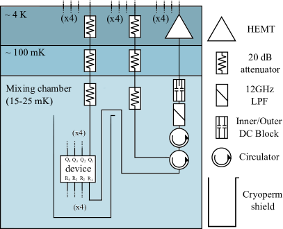
Experiments were all carried out during a single cooldown inside an Oxford Instruments Triton 500 dilution refrigerator, with a base stage temperature of . A diagram of the dilution refrigerator setup is included in the Appendices.
Acknowledgements.
This work has received funding from the United Kingdom Engineering and Physical Sciences Research Council under Grants No. EP/M013243/1, EP/N015118/1, EP/T001062/1, EP/M013294/1 and from Oxford Quantum Circuits Limited. T.T. acknowledges support from the Masason Foundation and the Nakajima Foundation. S.F. acknowledges support from the Swiss Study Foundation and the Bakala Foundation. B.V. acknowledges support from an EU Marie Sklodowska-Curie fellowship. We would like to thank Loxham Precision for their support with milling parameters and tooling.Appendix A Dilution refrigerator setup
Fig. A1 shows the experimental setup of the Oxford Instruments Triton 500 dilution refrigerator.
Appendix B Device enclosure and control wiring
Fig. A2 shows optical images of the device. In Fig. A2(A), the sealed base and lid parts are shown with the wiring piece for qubit control partially inserted such that the protruding inner conductors are visible. The wiring piece is made from oxygen-free copper to improve device thermalization. The coaxial cables that deliver control signals to qubits and resonators are non-magnetic silver-plated copper (SPC) UT47 coaxial cables with an outer diameter of . At the fridge-facing end, the coaxial cables are terminated with SMP connectors, which can be arranged into a lattice with a higher packing density than SMA connectors. At the circuit-facing end, the exposed inner conductors of these coaxial cables, having a diameter of , extend out a distance from the copper plate, where is defined in Fig. 2(A) of the main text. Each wiring piece is aligned to the lid and base parts by steel dowel pins. Fig. A2(B) shows an enlarged view of the extended inner conductors used for qubit control. The through holes in the lid that these inner conductors slot into are also visible, having a diameter of . A lateral misalignment of the inner conductors greater than will result in the inner conductors shorting to the device enclosure, causing the out-of-plane wiring to fail. Fig. A2(C) shows the fully assembled device, with the control wiring pieces for qubit control and resonator control both attached. The fasteners are made from titanium.
Appendix C Dephasing characterization measurements
Example Ramsey and Hahn echo experiments that were performed on are shown in Fig. A3. The pulse sequences for these experiments are shown in the insets. Ramsey experiments were repeated 21 times on each qubit taking approximately 2 hours per qubit. Hahn echo experiments were repeated 26 times on each qubit taking approximately 2 hours per qubit. Each Hahn echo experiment was repeated with an opposite phase on the final qubit control pulse, resulting in two exponential decay curves as shown in Fig. A3(C). These two curves were fit to and respectively, which improved the robustness of the extracted fit parameters A, B and .
Appendix D Qubit control line selectivity
Fig. A4 shows the measured Rabi oscillation rates in and when continuously driving these qubits on resonance through qubit control line 1 over a range of drive voltages . The fitted linear responses and are also shown.
The voltage at qubit control line satisfies where takes into account the attenuation between the room temperature generator and the device.
It is assumed that and are independent of the drive frequency over the range of qubit frequencies.
In the main text, it is stated that from the good fit of the Rabi rate to the function in the strong drive regime , it follows that , where . This is now discussed. An effective expression for the total drive Hamiltonian on qubit from qubit control line is given by
| (7) |
where in addition to the control line crosstalk , describes a coupling between qubit and qubit control line mediated through the transverse coupling between qubits and (and which is in general dependent on the state of qubit ). The phase accounts for any phase difference between and . A drive voltage at frequency will result in Rabi oscillations in qubit with a rate given by
| (8) |
In the low drive strength regime is approximately independent of , and for qubit in the ground state and is given by [61]
| (9) |
In the high drive strength regime , is dependent on the drive voltage , and can be numerically solved for using the semianalytical method introduced in Ref. [61]. The dashed green curve in Fig. A4(B) shows the predicted relationship between and using this semianalytical method to determine , assuming that (i.e. ) and that is in the ground state. The semianalytical model Hamiltonian is truncated to the first 10 levels, and is treated as a fit parameter, which is chosen such that the curve intersects the first data point. The obvious poor fit of this curve to the data is clear evidence that is not satisfied in the measured device. The blue curves show the predicted response for , for phase values . Again, is chosen such that the curves intersect the first data point. In this case, the non-linear contribution of still results in curves that differ significantly from the measured data. Since all of the measured Rabi rates show an excellent fit to the linear function , we infer that and hence that , consistent with the simulation predictions in Table 3. In this case, eq. 8 reduces to , resulting in the following expression for
| (10) |
which leads to the relation in the main text , where we restate for the reader that .
Appendix E Resonator control line selectivity
Fig. A5 shows the measured AC-Stark shifts in and when continuously driving resonators and through resonator control line 1 at frequency with , over a range of drive powers . The fitted linear responses and are also shown.
The voltage at resonator control line satisfies where takes into account the attenuation between the room temperature generator and the device, and where , with .
It is assumed that and are independent of the drive frequency over the range of resonator frequencies.
The average photon number in resonator due to a continuous drive through resonator control line at frequency is given by [36, 62, 33]
| (11) |
where is the effective frequency of resonator taking into account shifts due to (e.g.) the state of qubits. In the low photon number regime , where it is restated that , is to good approximation independent of the photon number . For a drive frequency , in eq. 11 becomes where . If qubit is in the first excited state, then . For , becomes effectively independent of the state of qubit . Note that is to an excellent approximation also independent of the state of other qubits, since for . In the case that additionally , eq. 11 takes the simple form
| (12) |
In the regime , the induced AC Stark-shift in qubit due to this population in resonator is given by [36]. Substituting eq. 12 and into this formula leads to the following expression for
| (13) |
which leads to the relation in the main text , where we restate for the reader that .
Appendix F Qubit-resonator crosstalk
In the experiment to bound the parasitic dispersive shift , resonator was populated with photons using a drive applied on resonance with its ground state frequency . The generator power required to populate resonator with photons using a continuous drive applied at frequency was calibrated in the following manner. Ramsey experiments were carried out on qubit while applying a continuous drive through resonator control line at frequency , over a range of drive powers .
The Ramsey decay rate was then fit to the formula as shown in Fig. A6. The photon number in resonator given qubit is in the ground state, , is (in the regime ) linearly related to the generator power through , where is given by
| (14) |
A derivation of eq. 14 is provided here. The generalized measurement induced dephasing rate of qubit under a drive at frequency is given by [36, 33]
| (15) |
where is the average photon number in resonator given that qubit is in the excited state. For a drive at frequency , the induced dephasing rate becomes
| (16) |
where has been used, which follows from eq. 11. We stress that this expression and eq. 16 are only valid for a drive applied at frequency . At times , the Ramsey dephasing rate of qubit under this dephasing drive is given by [36, 33], where is the dephasing rate due to all other mechanisms independent of the drive. Making the association and substituting this along with into eq. 16 then leads to eq. 14.
Assuming for the moment that the expression remains valid outside the regime , we calculate that the steady state photon numbers driven into each resonator in the qubit-resonator crosstalk experiment were: , where . However, the simple linear expression is generally only valid in the limit [36, 62, 33]. To determine a bound on parasitic dispersive shifts , we make the reasonable assumption that the linear relationship remained valid in this device for . Under this assumption, each resonator was driven with a photon number of at least (to within error) since the photon number is a monotonically increasing function with respect to the drive power. This leads to the bound in the main text.
Appendix G Correlated RB depolarizing parameters and crosstalk metric
The 15 parameters determined by correlated RB are shown in Table. AI. The error bars were found by a bootstrapping technique. First, a collection of resampled RB data sets were generated from the the measured RB data set, by resampling with replacement from the different Clifford sequences. Correlated RB analysis was then performed on each of these resampled data sets, resulting in values for each parameter, with the reported error being the standard deviation.
The 15 parameters were mapped directly onto 16 ( is now included) Pauli fixed-weight parameters using a transformation without fitting parameters [34]. The resulting values are shown in Fig. A7. These values should lie in the interval and satisfy [34]. The plotted error bars were estimated by mapping the collection of bootstrapped parameter sets onto a collection of bootstrapped parameter sets, and taking the standard deviation of each parameter. The crosstalk metric was then calculated using the formula [34]
| (17) |
where are Pauli fixed-weight parameters for an uncorrelated error channel such that for . These are treated as fitting parameters, and are chosen to minimize while being contrained to lie in the interval and satisfy . Since all the values should lie in the interval , the small negative values were set to zero when determining . A collection of values of were calculated from the bootstrapped parameter sets and the standard deviation was used to estimate the error. The result was . We expect that the error determined by this method is an underestimate as it neglects errors introduced by the negative values. In the main text, we therefore report that .
| Subspace | depolarizing parameter |
|---|---|
| 1000 | 0.99962(1) |
| 0100 | 0.99954(4) |
| 0010 | 0.99969(1) |
| 0001 | 0.99950(2) |
| 1100 | 0.99920(3) |
| 1010 | 0.99931(1) |
| 1001 | 0.99914(1) |
| 0110 | 0.99927(3) |
| 0101 | 0.99910(3) |
| 0011 | 0.99921(1) |
| 1110 | 0.99893(3) |
| 1101 | 0.99875(3) |
| 1011 | 0.99884(2) |
| 0111 | 0.99882(3) |
| 1111 | 0.99846(4) |
Appendix H Band structure simulations
Fig. A8(A)&(B) show the HFSS models used to simulate the band structure in Fig. 7 of the main text. The enclosure was modeled as a perfectly conducting material. The relative permittivity of the silicon substrate was taken to be [63], and the relative loss tangent was set to , neglecting internal losses. The qubit and resonator electrodes were included in the simulation and modeled as perfectly conducting 2D sheets using the ‘perfect E’ boundary condition. The qubit and resonator control line inner conductors were modeled as perfectly conducting material. The model dimensions are such that the infinite structure formed by tiling this model is identical to that formed by tiling the model shown in Fig. 7(A) of the main text. In the model shown in Fig. A8(A) the control ports were terminated with boundaries to simulate external losses out of the system. In the model shown in Fig. A8(B) the control ports were terminated using the ‘perfect E’ boundary condition to avoid convergence issues encountered with the Eigenmode solver.
Linked boundary condition (LBC) pairs were defined on the silicon and vacuum regions at the four faces of the models, using the so called ‘Master’ and ‘Slave’ boundary conditions. By changing the relative phase between Master and Slave pairs, the HFSS Eigenmode solver mapped out the band structure of the infinite structure formed by tiling the plane with the model.
The analytical predictions for the plasma frequency and band-curvature around the point , as well as the plasma skin depth, are discussed here. As a function of the radius and spacing of the pillar lattice, the plasma frequency was approximated using the following analytical formula [64, 65]
| (18) |
where and is a constant numerical factor approximately equal to . The predicted dispersion around the point in the presence of the pillar lattice was found using the following expansion [23]
| (19) |
where . This results in , where we restate for the reader that is defined by the relation . In the absence of the pillar lattice, the predicted dispersion around the point is given by , i.e. the dispersion of a plane wave propagating in the plane inside a medium with relative permittivity . The relative permittivity for the enclosure was modified by the presence of the vacuum region above the silicon substrate. The thickness of the silicon substrate is and the thickness of the vacuum region between the substrate and the enclosure lid is . Taking the cryogenic relative permittivity of silicon to be , the effective relative permittivity was then calculated as [23]
| (20) |
Inserting this into eq. 18 with and results in the predictions and that appear in the main text. Further inserting this value of into and taking results in the prediction that also appears in the main text.
We make the following observation regarding the effect of the vacuum region on cavity mediated crosstalk. In the regime , the plasma skin depth is given by , using eq. 18. This expression is independent of . Thus, in the regime , further reducing by increasing the thickness of the vacuum region is predicted to be an ineffective strategy for reducing the skin depth of cavity mediated crosstalk in this architecture.
Appendix I Radiative loss and transverse coupling simulations
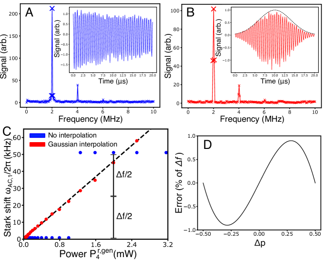
Fig. A8(C) shows the HFSS model used to simulate the parasitic transverse couplings and , and the radiatively limited relaxation time of qubits. The enclosure, silicon substrate, qubit and resonator electrodes, and control lines were all modeled identically to their counterparts in the band structure simulations. The control ports were terminated with boundaries to simulate external losses out of the system.
The Driven Terminal solver in HFSS was used to simulate the transverse couplings. In order to simulate between qubits and , all qubit electrode pairs were connected by lumped ports at the location of the Josephson junctions. The resonator electrode pairs were inductively disconnected to reduce simulation complexity. The transfer impedance between qubit ports and was simulated at a frequency of . The transfer impedances were then inserted into a simple impedance formula [31] to determine . To simulate between qubit and resonator , all resonator electrode pairs were directly connected by lumped ports (effects due to the spiral geometry of the resonator inductors were neglected), in addition to the lumped ports placed across qubit electrode pairs. The transfer impedance between qubit port and resonator port was then simulated at frequency values of and and the results were inserted into the same impedance formula to determine .
In order to simulate the radiatively limited lifetime of qubits, one qubit in the model was connected by a lumped port at the location of its Josephson junction, and the electrodes of the associated resonator were connected by a spiral inductor [as visible in Fig. A8(C)]. The remaining qubit and resonator electrode pairs were all inductively disconnected to reduce the simulation complexity. The impedance at the qubit port was then simulated over a range of frequencies using the fast frequency sweep functionality, and the radiatively limited lifetime was found using the method in Ref. [51]. The spiral inductor geometry was such that the simulated resonator frequency was , and the junction inductance was chosen such that .
Appendix J Ramsey interferometry frequency resolution improvement of fft using Gaussian interpolation
To find the resonator control line selectivities and to bound the parasitic dispersive shifts , it was necessary to determine the dominant frequency in Ramsey experiment time trace data. Fig. A9(A) shows the fast Fourier transform (fft) of a long Ramsey time trace measurement on . The principal peak of the fft, index , corresponds to the dominant oscillation frequency. The frequency separation of points in the fft, , is in this case . The dominant frequency can be estimated as , with a resolution of , which in this case is .
Following Ref. [60], the frequency resolution was greatly improved by applying a Gaussian window with standard deviation to the time trace data and then interpolating the ‘true’ dominant frequency value by using the fft signal amplitudes at the indices , denoted . The predicted frequency is given by where satisfies [60]
| (21) |
Assuming that the time trace data is a sinusoid with frequency , the frequency error of this Gaussian interpolation technique can also be found [60]. The predicted value of the frequency error as a function of for is plotted in Fig. A9(D). The maximum error is . This corresponds to a frequency resolution of approximately for as was used in the resonator control line selectivity experiments, and a maximum frequency resolution of approximately for as was used in the parasitic dispersive shift bound experiments. Note that these predicted resolutions are smaller (i.e. better) than the true resolutions as they neglect noise and exponential decay in the Ramsey time trace data.
The improvement in the frequency resolution afforded by this Gaussian windowing technique is shown in Fig. A9(B)&(C). Fig. A9(B) shows the fft of the same time trace data as that in Fig. A9(A), where now the time trace data has been windowed with a Gaussian function with . Notice the far larger signal amplitudes and in this fft. Fig. A9(C) shows the AC Stark shift while continuously driving through resonator control line 4 with generator power . Principal peak selection results in a frequency resolution of , whereas the Gaussian interpolation method achieves a frequency resolution of approximately . The linear fit to the interpolated frequencies provided the value of which was used to determine the resonator control line selectivity .
References
- Andersen et al. [2020] C. K. Andersen, A. Remm, S. Lazar, S. Krinner, N. Lacroix, G. J. Norris, M. Gabureac, C. Eichler, and A. Wallraff, Repeated quantum error detection in a surface code, Nature Physics 16, 875 (2020).
- Barends et al. [2014] R. Barends, J. Kelly, A. Megrant, A. Veitia, D. Sank, E. Jeffrey, T. C. White, J. Y. Mutus, A. G. Fowler, B. Campbell, et al., Superconducting quantum circuits at the surface code threshold for fault tolerance, Nature 508, 500 (2014).
- Fowler et al. [2012] A. G. Fowler, M. Mariantoni, J. M. Martinis, and A. N. Cleland, Surface codes: Towards practical large-scale quantum computation, Physical Review A 86, 032324 (2012).
- Bravyi and Kitaev [1998] S. B. Bravyi and A. Y. Kitaev, Quantum codes on a lattice with boundary, arXiv preprint quant-ph/9811052 (1998).
- Yanay et al. [2020] Y. Yanay, J. Braumüller, S. Gustavsson, W. D. Oliver, and C. Tahan, Two-dimensional hard-core bose–hubbard model with superconducting qubits, npj Quantum Information 6, 1 (2020).
- Gong et al. [2021] M. Gong, S. Wang, C. Zha, M.-C. Chen, H.-L. Huang, Y. Wu, Q. Zhu, Y. Zhao, S. Li, S. Guo, et al., Quantum walks on a programmable two-dimensional 62-qubit superconducting processor, Science (2021).
- Arute et al. [2019] F. Arute, K. Arya, R. Babbush, D. Bacon, J. C. Bardin, R. Barends, R. Biswas, S. Boixo, F. G. Brandao, D. A. Buell, et al., Quantum supremacy using a programmable superconducting processor, Nature 574, 505 (2019).
- Otterbach et al. [2017] J. Otterbach, R. Manenti, N. Alidoust, A. Bestwick, M. Block, B. Bloom, S. Caldwell, N. Didier, E. S. Fried, S. Hong, et al., Unsupervised machine learning on a hybrid quantum computer, arXiv preprint arXiv:1712.05771 (2017).
- Kjaergaard et al. [2020] M. Kjaergaard, M. E. Schwartz, J. Braumüller, P. Krantz, J. I.-J. Wang, S. Gustavsson, and W. D. Oliver, Superconducting qubits: Current state of play, Annual Review of Condensed Matter Physics 11, 369 (2020).
- Chen et al. [2014] Z. Chen, A. Megrant, J. Kelly, R. Barends, J. Bochmann, Y. Chen, B. Chiaro, A. Dunsworth, E. Jeffrey, J. Y. Mutus, et al., Fabrication and characterization of aluminum airbridges for superconducting microwave circuits, Applied Physics Letters 104, 052602 (2014).
- Huang et al. [2021] S. Huang, B. Lienhard, G. Calusine, A. Vepsäläinen, J. Braumüller, D. K. Kim, A. J. Melville, B. M. Niedzielski, J. L. Yoder, B. Kannan, et al., Microwave package design for superconducting quantum processors, PRX Quantum 2, 020306 (2021).
- Béjanin et al. [2016] J. Béjanin, T. McConkey, J. Rinehart, C. Earnest, C. McRae, D. Shiri, J. Bateman, Y. Rohanizadegan, B. Penava, P. Breul, et al., Three-dimensional wiring for extensible quantum computing: The quantum socket, Physical Review Applied 6, 044010 (2016).
- Bronn et al. [2018] N. T. Bronn, V. P. Adiga, S. B. Olivadese, X. Wu, J. M. Chow, and D. P. Pappas, High coherence plane breaking packaging for superconducting qubits, Quantum science and technology 3, 024007 (2018).
- Foxen et al. [2017] B. Foxen, J. Y. Mutus, E. Lucero, R. Graff, A. Megrant, Y. Chen, C. Quintana, B. Burkett, J. Kelly, E. Jeffrey, et al., Qubit compatible superconducting interconnects, Quantum Science and Technology 3, 014005 (2017).
- Yost et al. [2020] D. R. W. Yost, M. E. Schwartz, J. Mallek, D. Rosenberg, C. Stull, J. L. Yoder, G. Calusine, M. Cook, R. Das, A. L. Day, et al., Solid-state qubits integrated with superconducting through-silicon vias, npj Quantum Information 6, 1 (2020).
- Rosenberg et al. [2017] D. Rosenberg, D. Kim, R. Das, D. R. W. Yost, S. Gustavsson, D. Hover, P. Krantz, A. Melville, L. Racz, G. Samach, et al., 3d integrated superconducting qubits, npj quantum information 3, 1 (2017).
- Alfaro-Barrantes et al. [2020] J. Alfaro-Barrantes, M. Mastrangeli, D. Thoen, S. Visser, J. Bueno, J. Baselmans, and P. Sarro, Superconducting high-aspect ratio through-silicon vias with dc-sputtered al for quantum 3d integration, IEEE Electron Device Letters (2020).
- Vahidpour et al. [2017] M. Vahidpour, W. O’Brien, J. T. Whyland, J. Angeles, J. Marshall, D. Scarabelli, G. Crossman, K. Yadav, Y. Mohan, C. Bui, et al., Superconducting through-silicon vias for quantum integrated circuits, arXiv preprint arXiv:1708.02226 (2017).
- Lei et al. [2020] C. U. Lei, L. Krayzman, S. Ganjam, L. Frunzio, and R. J. Schoelkopf, High coherence superconducting microwave cavities with indium bump bonding, Applied Physics Letters 116, 154002 (2020).
- Brecht et al. [2017] T. Brecht, Y. Chu, C. Axline, W. Pfaff, J. Z. Blumoff, K. Chou, L. Krayzman, L. Frunzio, and R. J. Schoelkopf, Micromachined integrated quantum circuit containing a superconducting qubit, Physical Review Applied 7, 044018 (2017).
- Brecht et al. [2016] T. Brecht, W. Pfaff, C. Wang, Y. Chu, L. Frunzio, M. H. Devoret, and R. J. Schoelkopf, Multilayer microwave integrated quantum circuits for scalable quantum computing, npj Quantum Information 2, 1 (2016).
- Brecht et al. [2015] T. Brecht, M. Reagor, Y. Chu, W. Pfaff, C. Wang, L. Frunzio, M. H. Devoret, and R. J. Schoelkopf, Demonstration of superconducting micromachined cavities, Applied Physics Letters 107, 192603 (2015).
- Spring et al. [2020] P. A. Spring, T. Tsunoda, B. Vlastakis, and P. J. Leek, Modeling enclosures for large-scale superconducting quantum circuits, Physical Review Applied 14, 024061 (2020).
- Murray and Abraham [2016] C. E. Murray and D. W. Abraham, Predicting substrate resonance mode frequency shifts using conductive, through-substrate vias, Applied Physics Letters 108, 084101 (2016).
- Rahamim et al. [2017] J. Rahamim, T. Behrle, M. Peterer, A. D. Patterson, P. A. Spring, T. Tsunoda, R. Manenti, G. Tancredi, and P. J. Leek, Double-sided coaxial circuit qed with out-of-plane wiring, Applied Physics Letters 110, 222602 (2017).
- Patterson et al. [2019] A. D. Patterson, J. Rahamim, T. Tsunoda, P. A. Spring, S. Jebari, K. Ratter, M. Mergenthaler, G. Tancredi, B. Vlastakis, M. Esposito, et al., Calibration of a cross-resonance two-qubit gate between directly coupled transmons, Physical Review Applied 12, 064013 (2019).
- Koch et al. [2007] J. Koch, M. Y. Terri, J. M. Gambetta, A. A. Houck, D. I. Schuster, J. Majer, A. Blais, M. H. Devoret, S. M. Girvin, and R. J. Schoelkopf, Charge-insensitive qubit design derived from the cooper pair box, Physical Review A 76, 042319 (2007).
- Wang et al. [2015] C. Wang, C. Axline, Y. Y. Gao, T. Brecht, Y. Chu, L. Frunzio, M. H. Devoret, and R. J. Schoelkopf, Surface participation and dielectric loss in superconducting qubits, Applied Physics Letters 107, 162601 (2015).
- Reagor [2016] M. J. Reagor, Superconducting cavities for circuit quantum electrodynamics (Yale University, 2016).
- [30] IBM, Qiskit, open-source quantum computing software, https://qiskit.org/documentation/stubs/qiskit.ignis.verification.coherence_limit.html.
- Solgun et al. [2019] F. Solgun, D. P. DiVincenzo, and J. M. Gambetta, Simple impedance response formulas for the dispersive interaction rates in the effective hamiltonians of low anharmonicity superconducting qubits, IEEE transactions on microwave theory and techniques 67, 928 (2019).
- [32] Ansys, Ansys HFSS (High Frequency Structural Simulator), https://www.ansys.com.
- Blais et al. [2020] A. Blais, A. L. Grimsmo, and A. Wallraff, Circuit quantum electrodynamics, Reviews of modern Physics 93, 025005 (2020).
- McKay et al. [2020] D. C. McKay, A. W. Cross, C. J. Wood, and J. M. Gambetta, Correlated randomized benchmarking, arXiv preprint arXiv:2003.02354 (2020).
- Gambetta et al. [2012] J. M. Gambetta, A. D. Córcoles, S. T. Merkel, B. R. Johnson, J. A. Smolin, J. M. Chow, C. A. Ryan, C. Rigetti, S. Poletto, T. A. Ohki, et al., Characterization of addressability by simultaneous randomized benchmarking, Physical review letters 109, 240504 (2012).
- Gambetta et al. [2006] J. M. Gambetta, A. Blais, D. I. Schuster, A. Wallraff, L. Frunzio, J. Majer, M. H. Devoret, S. M. Girvin, and R. J. Schoelkopf, Qubit-photon interactions in a cavity: Measurement-induced dephasing and number splitting, Physical Review A 74, 042318 (2006).
- Chow et al. [2009] J. M. Chow, J. M. Gambetta, L. Tornberg, J. Koch, L. S. Bishop, A. A. Houck, B. R. Johnson, L. Frunzio, S. M. Girvin, and R. J. Schoelkopf, Randomized benchmarking and process tomography for gate errors in a solid-state qubit, Physical review letters 102, 090502 (2009).
- Motzoi et al. [2009] F. Motzoi, J. M. Gambetta, P. Rebentrost, and F. K. Wilhelm, Simple pulses for elimination of leakage in weakly nonlinear qubits, Physical review letters 103, 110501 (2009).
- McKay et al. [2017] D. C. McKay, C. J. Wood, S. Sheldon, J. M. Chow, and J. M. Gambetta, Efficient z gates for quantum computing, Physical Review A 96, 022330 (2017).
- Wood and Gambetta [2018] C. J. Wood and J. M. Gambetta, Quantification and characterization of leakage errors, Physical Review A 97, 032306 (2018).
- Pendry et al. [1996] J. B. Pendry, A. J. Holden, W. J. Stewart, and I. Youngs, Extremely low frequency plasmons in metallic mesostructures, Physical review letters 76, 4773 (1996).
- Pendry et al. [1998] J. B. Pendry, A. J. Holden, D. J. Robbins, and W. J. Stewart, Low frequency plasmons in thin-wire structures, Journal of Physics: Condensed Matter 10, 4785 (1998).
- Müller et al. [2019] C. Müller, J. H. Cole, and J. Lisenfeld, Towards understanding two-level-systems in amorphous solids: insights from quantum circuits, Reports on Progress in Physics 82, 124501 (2019).
- Burnett et al. [2019] J. J. Burnett, A. Bengtsson, M. Scigliuzzo, D. Niepce, M. Kudra, P. Delsing, and J. Bylander, Decoherence benchmarking of superconducting qubits, npj Quantum Information 5, 1 (2019).
- Klimov et al. [2018] P. V. Klimov, J. Kelly, Z. Chen, M. Neeley, A. Megrant, B. Burkett, R. Barends, K. Arya, B. Chiaro, Y. Chen, et al., Fluctuations of energy-relaxation times in superconducting qubits, Physical review letters 121, 090502 (2018).
- Müller et al. [2015] C. Müller, J. Lisenfeld, A. Shnirman, and S. Poletto, Interacting two-level defects as sources of fluctuating high-frequency noise in superconducting circuits, Physical Review B 92, 035442 (2015).
- Serniak et al. [2018] K. Serniak, M. Hays, G. de Lange, S. Diamond, S. Shankar, L. Burkhart, L. Frunzio, M. Houzet, and M. H. Devoret, Hot nonequilibrium quasiparticles in transmon qubits, Physical review letters 121, 157701 (2018).
- Catelani et al. [2011] G. Catelani, R. J. Schoelkopf, M. H. Devoret, and L. I. Glazman, Relaxation and frequency shifts induced by quasiparticles in superconducting qubits, Physical Review B 84, 064517 (2011).
- Serniak et al. [2019] K. Serniak, S. Diamond, M. Hays, V. Fatemi, S. Shankar, L. Frunzio, R. J. Schoelkopf, and M. H. Devoret, Direct dispersive monitoring of charge parity in offset-charge-sensitive transmons, Physical Review Applied 12, 014052 (2019).
- Barends et al. [2011] R. Barends, J. Wenner, M. Lenander, Y. Chen, R. C. Bialczak, J. Kelly, E. Lucero, P. O’Malley, M. Mariantoni, D. Sank, et al., Minimizing quasiparticle generation from stray infrared light in superconducting quantum circuits, Applied Physics Letters 99, 113507 (2011).
- Nigg et al. [2012] S. E. Nigg, H. Paik, B. Vlastakis, G. Kirchmair, S. Shankar, L. Frunzio, M. H. Devoret, R. J. Schoelkopf, and S. M. Girvin, Black-box superconducting circuit quantization, Physical Review Letters 108, 240502 (2012).
- Houck et al. [2008] A. A. Houck, J. A. Schreier, B. R. Johnson, J. M. Chow, J. Koch, J. M. Gambetta, D. I. Schuster, L. Frunzio, M. H. Devoret, S. M. Girvin, et al., Controlling the spontaneous emission of a superconducting transmon qubit, Physical review letters 101, 080502 (2008).
- Wang et al. [2019] Z. Wang, S. Shankar, Z. Minev, P. Campagne-Ibarcq, A. Narla, and M. H. Devoret, Cavity attenuators for superconducting qubits, Physical Review Applied 11, 014031 (2019).
- Heinsoo et al. [2018] J. Heinsoo, C. K. Andersen, A. Remm, S. Krinner, T. Walter, Y. Salathé, S. Gasparinetti, J.-C. Besse, A. Potočnik, A. Wallraff, et al., Rapid high-fidelity multiplexed readout of superconducting qubits, Physical Review Applied 10, 034040 (2018).
- Walter et al. [2017] T. Walter, P. Kurpiers, S. Gasparinetti, P. Magnard, A. Potočnik, Y. Salathé, M. Pechal, M. Mondal, M. Oppliger, C. Eichler, et al., Rapid high-fidelity single-shot dispersive readout of superconducting qubits, Physical Review Applied 7, 054020 (2017).
- Wilen et al. [2021] C. Wilen, S. Abdullah, N. Kurinsky, C. Stanford, L. Cardani, G. d’Imperio, C. Tomei, L. Faoro, L. Ioffe, C. Liu, et al., Correlated charge noise and relaxation errors in superconducting qubits, Nature 594, 369 (2021).
- Martinis [2021] J. M. Martinis, Saving superconducting quantum processors from decay and correlated errors generated by gamma and cosmic rays, npj Quantum Information 7, 1 (2021).
- Dolan and Dunsmuir [1988] G. J. Dolan and J. H. Dunsmuir, Very small ( nm) lithographic wires, dots, rings, and tunnel junctions, Physica B: Condensed Matter 152, 7 (1988).
- Wallraff et al. [2005] A. Wallraff, D. I. Schuster, A. Blais, L. Frunzio, J. Majer, M. H. Devoret, S. M. Girvin, and R. J. Schoelkopf, Approaching unit visibility for control of a superconducting qubit with dispersive readout, Physical review letters 95, 060501 (2005).
- Gasior and Gonzalez [2004] M. Gasior and J. L. Gonzalez, Improving FFT frequency measurement resolution by parabolic and gaussian interpolation, Tech. Rep. (2004).
- Tripathi et al. [2019] V. Tripathi, M. Khezri, and A. N. Korotkov, Operation and intrinsic error budget of a two-qubit cross-resonance gate, Physical Review A 100, 012301 (2019).
- Boissonneault et al. [2010] M. Boissonneault, J. M. Gambetta, and A. Blais, Improved superconducting qubit readout by qubit-induced nonlinearities, Physical review letters 105, 100504 (2010).
- Krupka et al. [2006] J. Krupka, J. Breeze, A. Centeno, N. Alford, T. Claussen, and L. Jensen, Measurements of permittivity, dielectric loss tangent, and resistivity of float-zone silicon at microwave frequencies, IEEE Transactions on microwave theory and techniques 54, 3995 (2006).
- Belov et al. [2002] P. A. Belov, S. A. Tretyakov, and A. J. Viitanen, Dispersion and reflection properties of artificial media formed by regular lattices of ideally conducting wires, Journal of electromagnetic waves and applications 16, 1153 (2002).
- Krynkin and McIver [2009] A. Krynkin and P. McIver, Approximations to wave propagation through a lattice of dirichlet scatterers, Waves in Random and Complex Media 19, 347 (2009).