Variability of electron and hole spin qubits due to interface roughness and charge traps
Abstract
Semiconductor spin qubits may show significant device-to-device variability in the presence of spin-orbit coupling mechanisms. Interface roughness, charge traps, layout or process inhomogeneities indeed shape the real space wave functions, hence the spin properties. It is, therefore, important to understand how reproducible the qubits can be, in order to assess strategies to cope with variability, and to set constraints on the quality of materials and fabrication. Here we model the variability of single qubit properties (Larmor and Rabi frequencies) due to disorder at the Si/SiO2 interface (roughness, charge traps) in metal-oxide-semiconductor devices. We consider both electron qubits (with synthetic spin-orbit coupling fields created by micro-magnets) and hole qubits (with intrinsic spin-orbit coupling). We show that charge traps are much more limiting than interface roughness, and can scatter Rabi frequencies over one order of magnitude. We discuss the implications for the design of spin qubits and for the choice of materials.
I Introduction
Spins in semiconductor quantum dots have emerged as a promising platform for quantum technologies.Loss and DiVincenzo (1998); Hanson et al. (2007) SiliconPla et al. (2012); Zwanenburg et al. (2013) and GermaniumScappucci et al. (2020) are particularly attractive host materials because their main isotopes are free of nuclear spins that may interfere with the electron spins. Record spin lifetimes have thus been measured in isotopically purified 28Si samples.Tyryshkin et al. (2012); Veldhorst et al. (2014) High fidelity single and two qubit gates have been reported in a variety of silicon/silicon oxide and silicon/germanium devices,Kawakami et al. (2014); Veldhorst et al. (2015a); Kawakami et al. (2016); Takeda et al. (2016); Yoneda et al. (2018); Watson et al. (2018); Zajac et al. (2018); Huang et al. (2019); Xue et al. (2019); Yang et al. (2020); Petit et al. (2020) and, more recently, a four qubit processor has been demonstrated in germanium (with hole spins).Hendrickx et al. (2021)
The spin carrier can indeed be either an electron or a hole.Hendrickx et al. (2021); Maurand et al. (2016); Crippa et al. (2018); Watzinger et al. (2018); Hendrickx et al. (2020a, b); Camenzind et al. (2021) Electrons in the conduction band of silicon and germanium undergo much weaker spin-orbit coupling (SOC) than holes in the valence band.Winkler (2003); Kloeffel et al. (2011, 2018) Therefore, electron spin qubits are better protected against electrical noise and undesirable interactions with, e.g., phonons. They tend to show, as a consequence, longer coherence and relaxation times than hole “spin-orbit” qubits.Li et al. (2020); Lawrie et al. (2020); Ciriano-Tejel et al. (2021) On the other hand, electron spin qubits can hardly be manipulatedCorna et al. (2018) electrically using Electric Dipole Spin Resonance (EDSR).Rashba and Efros (2003); Golovach et al. (2006); Rashba (2008) To enable EDSR, an artificial SOC can be synthesized with micro-magnets that generate a gradient of magnetic field.Tokura et al. (2006); Pioro-Ladrière et al. (2007, 2008); Kawakami et al. (2014, 2016); Takeda et al. (2016); Yoneda et al. (2018); Watson et al. (2018); Zajac et al. (2018); Xue et al. (2019); Yang et al. (2020) The real space motion of the electron in this gradient indeed translates into an effective time-dependent magnetic field in the frame of the carrier, acting on its spin. Electrically driven spin rotations with Rabi frequencies up to a few MHz can be achieved that way in electron spin qubits (while tens of MHz are typically reported for holes with intrinsic SOC). Anyhow, introducing artificial SOC enhances the interactions of the spin with noise and phonons and tends to decrease the lifetimes of the qubits. The strength of SOC can be controlled by confinement and strains in hole spin-orbit qubits,Michal et al. (2021) while it is set by the micromagnet design in electron spin qubits.
Another consequence of SOC for spin qubits is variability: the spin properties depend on the real space wave function, hence on inhomogeneities on a global scale (device-to-device variations in layout and characteristic sizes, wafer scale process fluctuations), and on a local scale (disorders such as interface roughness and charge traps). Such short range fluctuations are particularly annoying because they are random and cannot, therefore, be accounted for a priori in the design. As a consequence, each qubit must, in practice, be characterized individually before operating the quantum processor. While manageable for a few qubits, this may become a daunting bottleneck on the scale of hundreds of devices, especially if device-to-device variations are very large and cannot be at least partly compensated by bias adjustments or control software.
There is evidence in the literature that present spin qubits (with intrinsic or artificial SOC) show significant variability.Watson et al. (2018); Yang et al. (2020); Hendrickx et al. (2020b); Camenzind et al. (2021); Zwerver et al. (2021) While the design of these devices is often responsible for part of this variability (non equivalent gate layouts for each qubit for example), it is important to understand how reproducible the qubits can be in the presence of uncontrolled local disorder, in order to set constraints on the quality of materials and fabrication.
The variability of metal-oxide-semiconductor (MOS) transistors has been extensively investigated and modeled,Bernstein et al. (2006); Roy et al. (2006); Asenov et al. (2009); Mezzomo et al. (2011) yet systematic studies on semiconductor spin qubits are still scarce.Bourdet and Niquet (2018); Ibberson et al. (2018); Wu and Guo (2020); Simion et al. (2020) In this work, we specifically model two sources of disorder at the Si/SiO2 interface, interface roughness and charge traps (dangling bond defects), that are ubiquitous in MOS spin qubits. We focus on single qubit properties and discuss the distribution of the Zeeman splittings/Larmor frequencies and of the Rabi frequencies as a function of the strength of the disorder (height and lateral extent of the interface roughness fluctuations, density of traps). The speed of one qubit gates in a quantum processor will indeed be limited by the smallest Rabi frequencies, while the overall lifetimes can be limited by the largest ones (since faster qubits are better coupled to the electric field and may, therefore, be more sensitive to noise). Also, large deviations of the individual Larmor and Rabi frequencies will complicate the management of radio-frequency control signals on the chip. We consider spin qubits in one-dimensional silicon-on-insulator channels as prototypical devices but most conclusions are generic and apply to other device layouts. We compare hole spin qubits with intrinsic SOC and electron spin qubits with artificial SOC and highlight the similarities and differences between the two kinds of carriers and SOC. We show that charge disorder in the vicinity of the qubits is much more critical than interface roughness, and can scatter Rabi frequencies over more than one order of magnitude. We finally discuss the implications for qubit lifetimes and performances, for device design and materials, and some solutions to mitigate variability.
II Devices and methodology
In this section, we describe the devices and the methodology used in this study.
II.1 Devices
We have considered two classes of silicon devices: hole spin qubits with intrinsic SOC and electron spin qubits with a synthetic SOC created by micro-magnets.
II.1.1 Hole devices
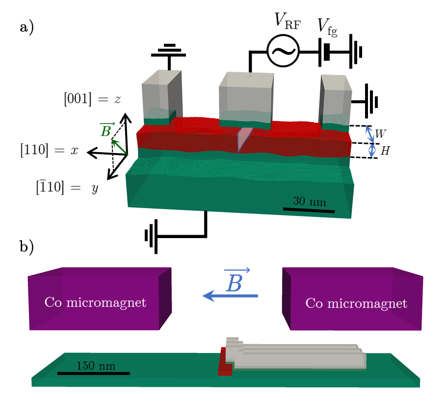
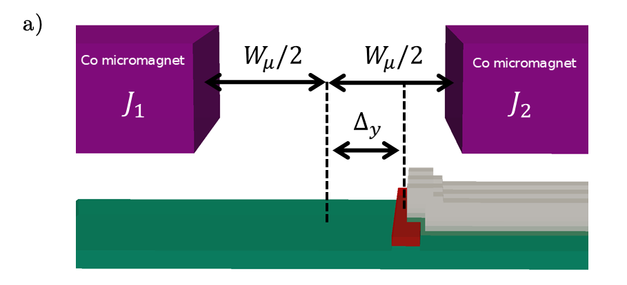
The hole spin qubits are similar to those of Refs. Maurand et al., 2016; Venitucci et al., 2018; Li et al., 2020 and are shown in Fig. 1a. The devices are made of a -oriented silicon nanowire channel with width nm [ facets] and height nm [ facets] on top of a 25 nm thick buried silicon oxide and a silicon substrate. A 30 nm long central gate overlapping half of the nanowire controls a quantum dot. It is insulated from the channel by 5 nm of SiO2. Two other gates on the left and right mimic neighboring qubits. The whole device is embedded in Si3N4. The silicon substrate can be used as a back gate, grounded throughout this study. The left and right gates are also grounded, and the depth of the dot potential is controlled by the central gate voltage .
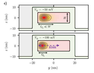
Poisson’s equation for the single-particle potential in the empty dots is solved with a finite volumes method (assuming dielectric constants , , and ). The ground-state Kramers pair is then computed with a finite-differences 6 bands modelVenitucci et al. (2018) (assuming Luttinger parameters , , , split-off energy meV, and Zeeman parameter ).111The valence band edge energy is set to eV in hole qubits; likewise, the conduction edge energy is set to eV in electron qubits. This Kramers pair splits at finite magnetic field and can be manipulated electrically with a radio-frequency (RF) signal on the central gate, resonant with the Zeeman splitting between the “” and “” (pseudo-)spin states. The single qubit can hence be characterized by the Larmor frequency , and by the Rabi frequency , which quantifies the speed of the pseudo-spin rotations under electrical driving. Both are computed numerically with the -matrix formalism of Ref. Venitucci et al., 2018. This device operates in the “-tensor magnetic resonance” (-TMR) mode,Kato et al. (2003) where the RF electric field from the central gate essentially modulates the lateral confinement (see Fig. 1c), hence the principal -factors of the dot owing to the strong, intrinsic spin-orbit coupling in the valence bands.Venitucci et al. (2018); Venitucci and Niquet (2019); Michal et al. (2021) We have verified that similar conclusions are achieved when the hole is driven as a whole along the channel by a RF signal on the left and right gates (“iso-Zeeman EDSR modeMichal et al. (2021)”, see Appendix E).
The Larmor and Rabi frequencies of hole qubits are strongly dependent on the orientation of the external magnetic field . They have been computed for along , which is near the optimal direction in the -TMR mode (see axes in Fig. 1).Venitucci et al. (2018); Venitucci and Niquet (2019); Michal et al. (2021) is proportional to the amplitude of the magnetic field, and to both and the amplitude of the driving signal on the central gate. Therefore, and are normalized to reference T and mV throughout this work.
II.1.2 Electron devices
Intrinsic spin-orbit coupling is inefficient in the conduction band of silicon owing, in part, to the indirect nature of the band gap.Corna et al. (2018) Therefore, a synthetic spin-orbit coupling must be introduced in order to allow for the electrical manipulation of electron spin qubits. This can be achieved by placing the qubits in a gradient of magnetic field provided by micro-magnets.Pioro-Ladrière et al. (2008); Kawakami et al. (2014); Takeda et al. (2016); Yoneda et al. (2018); Kawakami et al. (2016) The RF electric field from the gate shakes the electron in this gradient; this translates into a time-dependent magnetic field in the frame of the electron, which acts on its spin. We add, therefore, two semi-infinite Co micro-magnets nm above the channel. They are nm thick and are split apart by nm (Fig. 1b). We assume that the magnetic polarization T of the Co magnetsNeumann and Schreiber (2015) is saturated in a transverse, external magnetic field T along . The vector potential created by these micro-magnets is calculated with a technique similar to Refs. Yang et al., 1990 and Goldman et al., 2000 (see Appendix A); and its action on the real space and spin motions is described by an anisotropic effective mass model for the Z-valleys (with longitudinal mass and transverse mass , see Appendix B). We discard spin-valley and valley-orbit interactions in this study. The effects of interface roughness/steps and charge traps on the valley splitting have been discussed, for example, in Refs. Culcer et al., 2010; Jiang et al., 2012; Bourdet and Niquet, 2018; Ibberson et al., 2018; Abadillo-Uriel et al., 2018; Tariq and Hu, 2019; Hosseinkhani and Burkard, 2020 (see further discussion in Section V.1).
II.2 Disorders and methodology
In this work, we focus on two kinds of disorder at the Si/SiO2 interface: interface roughness and charge traps ( defects). We also briefly address disorder in the micro-magnets in Appendix D.
II.2.1 Interface roughness
Interface roughness is explicitly added in the solvers for Poisson’s equation and for the 6 bands or effective mass models. For that purpose, samples of roughness are randomly generated on each facet of the wire with a target Gaussian auto-correlation function:Goodnick et al. (1985)
| (1) |
where is the out-of-plane displacement of the interface, and are in-plane positions, and denotes an ensemble average. is the rms amplitude of the roughness, and is a correlation length that characterizes the lateral extent of the fluctuations. The samples are generated in Fourier space, then transformed to real space, along the lines of Ref. Niquet et al., 2014.
In micro-electronics grade devices, atomic scale TEM images and room-temperature mobility measurements suggest in the nm range and in the 1 to 4 nm range.Goodnick et al. (1985); Pirovano et al. (2000); Esseni et al. (2003); Nguyen et al. (2014); Bourdet et al. (2016); Zeng et al. (2017a) However, the interface roughness limited mobility is typically measured at high carrier density, and therefore probes short length scales fluctuations, whereas spin qubits operate at low carrier density, and are thus presumably more sensitive to longer length scale fluctuations (as revealed, for example, by atomic force microscopyPirovano et al. (2000)). We have, therefore, varied between 1 and 30 nm, in order to span the experimentally relevant range and allow for a systematic exploration of the trends.
II.2.2 Charge traps
The Si/SiO2 interface separates a crystalline and an amorphous material, and is therefore prone to be defective. The prototype of these defects is the dangling bond () at the interface.Poindexter et al. (1984); Gerardi et al. (1986); Poindexter (1989); Helms and Poindexter (1994); Thoan et al. (2011) defects are amphoteric: they trap electrons on shallow to deep acceptor levels in -type devices, and trap holes on donor levels in -type devices. For simplicity, we model the charged defects as negative () point charges at the interface in electron spin qubits, and as positive () point charges in hole spin qubits, with densities ranging from to cm-2. These densities are, again, typical of micro-electronics grade interfaces.Bauza (2002); Brunet et al. (2009); Pirro et al. (2016); Vermeer et al. (2021) Our point charges model neglects the finite extension of the bound charge density around the defects; however, this is little relevant as the majority carriers in the dots get repelled by a charged , and, therefore, do not probe much the Coulomb singularity.
II.2.3 Methodology
The Larmor and Rabi frequencies are collected on sets on random samples of disorder (either interface roughness or charge traps).222We model one device at a time, with a different seed for the random number generator used by the geometry builder. Then the average Larmor or Rabi frequency , and its standard deviation are estimated as:333The factor (instead of ) on the denominator of Eq. (2b) follows from the definition of the “unbiased” estimate of the variance. This so-called Bessel correction does not make significant differences given the large data sets considered here ().
| (2a) | ||||
| (2b) | ||||
where the are the sampled frequencies. We characterize the variability by the relative standard deviation (RSD):
| (3) |
and by the inter-quartile range:
| (4) |
where is the frequency such that a proportion of the devices have . Therefore, 50% of the qubits lie within the IQR. Confidence intervals on , and the IQR are estimated using a percentile bootstrap (resampling) method.Davison and Hinkley (1997)
III Interface roughness
III.1 Holes
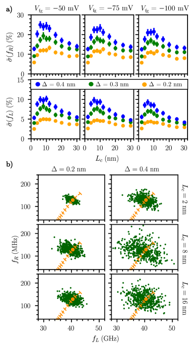
The RSD of the Rabi frequency and the RSD of the Larmor frequency of rough hole qubits are plotted as a function of for different and front gate voltages in Fig. 2a. They are normalized with respect to the average Rabi frequency and average Larmor frequency , which are very close to the Rabi frequency and Larmor frequency of the pristine device given in Table 1. The inter-quartile ranges are and , as expected for quasi-normal distributions.
| (mV) | (GHz) | (MHz) | (nm) |
|---|---|---|---|
| 40.46 | 128.47 | 3.28 | |
| 37.62 | 84.00 | 2.71 | |
| 36.06 | 56.19 | 2.38 |
The interface roughness primarily modulates the thickness of the channel. This alters the shape of the hole envelopes, hence the dipole or momentum matrix elements relevant for the Larmor and Rabi frequencies.Michal et al. (2021) This will be further analyzed in section III.3.
On the one hand, the variability increases, as expected, with the rms amplitude of the interface roughness fluctuations (almost linearly in this range). On the other hand, the variability shows a non-monotonic behavior with respect to the correlation length of the fluctuations, and peaks near nm. Indeed, fluctuations with length scales much shorter than the characteristic size of the dot tend to be averaged out and have little effect on the envelope functions of the holes. On the opposite, the interfaces become flat again on the scale of the dot when is much greater than the gate dimensions. Yet the variability does not tend to zero when : in fact, the thickness and width of the channel can still vary from device to device (with rms ) as top/down, left/right interface fluctuations are uncorrelated. The variability is maximal when the length scale of the fluctuations is comparable with the size of the dot (see section III.3).
As the front gate voltage is made further negative, the dot gets squeezed on the side of the channel by the lateral electric field (see Fig. 1c and Table 1).Venitucci et al. (2018); Venitucci and Niquet (2019) In this regime, the electric confinement length shall prevail over the characteristic scales of disorder on the top and bottom facets of the channel. The absolute standard deviations and , are, therefore, expected to decrease. However, also decreases continuously with increasingly negative because the strongly confined dot can hardly be shaken anymore by the RF electric field.Venitucci and Niquet (2019); Michal et al. (2021) As a consequence, the RSD shows a rather weak scaling with . The RSD exhibits an even weaker scaling even though the Larmor frequency remains finite at large negative . As discussed in III.3, this results from the increasing role of the disorder on the side facets.
For a rms nm, can be as large as , and as large as ( mV). The distribution of devices in the plane is plotted in Fig. 2b. There are no clear correlations between the deviations of Larmor and Rabi frequencies. The line of the pristine device is also reported on this figure. It outlines the average electrical tunability of the Larmor and Rabi frequencies. The deviations of Larmor frequencies must, in particular, be correctable if one wishes to address all qubits at a well defined RF frequency. The extent of bias corrections is, however, limited by the stability diagram of the device. Assuming a charging energy meV typical for these qubits, the range of gate voltage giving rise to chemical potential shifts in the dot is only meV. This limitation can nonetheless be overcome if inter-dot tunneling can be cut down sufficiently during single qubit operations. The deviations of Rabi frequencies may also be corrected by tuning the driving RF power for each qubit. This will be further discussed in section V.
III.2 Electrons
The data for electron qubits are shown in Fig. 3.
| (mV) | (GHz) | (MHz) | (nm) |
|---|---|---|---|
| 35.837 | 3.20 | 5.20 | |
| 35.845 | 2.22 | 4.69 | |
| 35.853 | 1.48 | 4.21 |
First of all, the Rabi frequencies of the pristine electron qubits (Table 2, in the MHz range) are much smaller than the Rabi frequencies of the pristine hole qubits (Table 1, in the tens of MHz range). These ranges are consistent with the Rabi frequencies measured in electron and hole spin qubits with different layouts.Kawakami et al. (2016); Watson et al. (2018); Yang et al. (2020); Maurand et al. (2016); Watzinger et al. (2018); Hendrickx et al. (2020b) Intrinsic spin-orbit coupling in the valence band is indeed, much more efficient than synthetic spin-orbit coupling in the conduction band. As a consequence, fast electrical driving calls for much larger real space motion (larger electric dipoles) in electron than in hole qubits, hence for larger/shallower dots. For the sake of consistency, we nonetheless compare electron and hole qubits with the same topology and structural dimensions here. Alternatively, the Rabi frequencies may be increased using stronger micro-magnets or bringing them closer to the qubits, when technologically feasible.
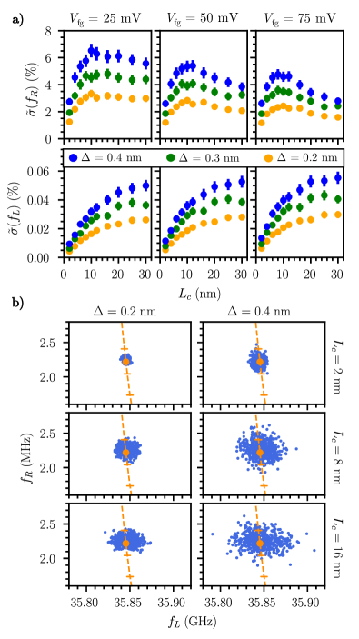
The variability of Larmor frequencies is as low as , but increases monotonously and saturates at large . It results from the vertical displacement of the dot as a whole in the gradient of magnetic field, induced by the interface roughness (see discussion in the next section).
The trends for the Rabi frequencies are the same as in hole qubits. The dependence of on gate voltage is slightly stronger for electrons than for holes; yet variability remains much smaller in electron qubits ( at nm and mV). We emphasize, though, that electron qubits are subject to additional sources of variability (e.g., alignment and homogeneity of the micro-magnetsYoneda et al. (2015); Simion et al. (2020)) that will be discussed in section V.1.
We analyse below the mechanisms responsible for variability and the differences between electron and hole qubits.
III.3 Mechanisms responsible for the variability
The electrons and holes are confined in the cross section of the channel by the vertical component and the lateral component of the electric field from the central gate. The strength of this electric field can, therefore, be characterized by the electric confinement lengths and , where is the vertical confinement mass along , and the in-plane mass.Michal et al. (2021) In the regimes explored in this work, while : the vertical confinement is dominated by the structure, while the in-plane confinement is dominated by the electric field (see Fig. 1c).
When , the interface roughness on the main top and bottom facets essentially modulates the thickness of the channel and the associated structural confinement energy . Therefore, in a single band model, long wavelength thickness fluctuations of translate into a potential
| (5) |
for the motion in the weakly confined plane.Sakaki et al. (1987); Uchida and Takagi (2003); Jin et al. (2007) In the opposite limit , would be dominated by the fluctuations of the position of the top interface in the vertical electric field. This regime is, however, more relevant for the iso-Zeeman driving mode of the holes (whose optimum is at strong field), and for the contribution of the side facets (whose role is discussed below).
The dot essentially oscillates along when the driving RF signal is applied to the central gate because the electric dipole is small along the strong confinement axis . The model for the electron qubits developed in Appendix B shows that the Rabi frequency of the electrons is then proportional to , where is the expectation value of the in-plane coordinate in the ground-state at zero magnetic field. The interface roughness shapes the envelope function of the electron in the plane hence the electrical response of the dot.
In the simplest models for the dot (hard-wall or harmonic confinement potential with homogeneous electric field along ),Venitucci and Niquet (2019); Michal et al. (2021) a dimensional analysis of the perturbation series for suggests that , where is the extension of the dot along : the stronger the confinement, the weaker the electrical response. Although the disordered potential considered here is rather complex, we can still expect correlations between the lateral size of the dot and the Rabi frequency.
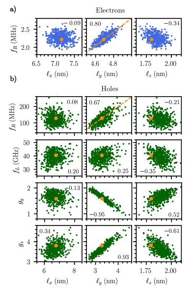
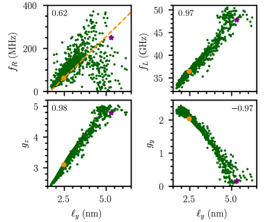
In order to highlight such correlations, we have plotted the Rabi frequency of the electron qubits as a function of the extensions , , and of the ground-state in Fig. 4a ( mV, nm, nm). The correlation coefficient between the abscissas ( or ) and the ordinates (), defined as:
| (6) |
is reported in each panel ( for uncorrelated and for linearly correlated and ). The correlations are much more significant between and than between and or , and follow approximately the relation expected from the dependence of (with , , and the extension of the ground-state in the pristine device). This supports the conclusion that the Rabi frequency is primarily modulated by the distortions of the dot along induced by the interface roughness. Note that the distribution of is skewed towards large , as the electron tends to localize in the thickest parts of the channel.444As a matter of fact, in a thin film with thickness . Since 95% of the thickness fluctuations lie within a range, and the electron/hole tends to localize in the thickest parts of the channel (), we expect nm, in agreement with Fig. 4
A simple analytical model for variability in a parabolic in-plane confinement potential, based on first-order perturbation theory, is discussed in Appendix C. This model explains most trends outlined above, even though confinement is highly anharmonic in the present devices. It confirms, in particular, that in rough films with thickness , as evidenced by Fig. 5. It also highlights that increases, in general, with the in-plane mass : the heavier the particles, the stronger they localize in the disorder. Finally, this model shows that the variability peaks when : fluctuations with wavelengths comparable to the size of the dot are expected to have the largest impact on its shape. The data of Fig. 3 peak at a slightly larger , owing, likely, to the anharmonicity of the in-plane confinement.
The analysis is more intricate for holes. The model of Ref. Michal et al., 2021 suggests that the Rabi frequency of the holes is inversely proportional to the gap between the heavy- and light-hole sub-bands, and proportional to , where can range from 1 () to 4 (). This behavior essentially results from the fact that instead of , where and the expectation value is computed for the ground-state heavy-hole envelope function. We may, therefore, expect correlations between and and/or . Figure 4b actually shows stronger correlations with () than with . The variability of the Rabi frequency is still, therefore, dominated by fluctuations of the in-plane size of the dot (at least for nm).
As for the Larmor frequency of electrons, depends on the position of the dot in the inhomogeneous field of the micro-magnets. The largest components of the gradient are (see Appendix A), but only the latter gives rise to first-order variations of the Larmor frequency in a static magnetic field along (while the former is responsible for the Rabi oscillations). As a consequence, the Larmor frequency correlates with instead of . The spread of is expected to grow monotonously with increasing ; when , the roughness profile becomes flat again on the scale of the dot so that
| (7) |
where and are the positions of the bottom and top interfaces. As (the interfaces being uncorrelated),
| (8) |
where is the total (external and micro-magnets) field along at the center of the channel. In the present layout, remains small because the inhomogeneous component of the magnetic field is much lower than the external magnetic field T.
For holes, the heavy-hole ground state gets mixed with a light-hole component by the electric field ,Venitucci et al. (2018) due to the competition between vertical (mostly structural) confinement along and lateral (electric) confinement along . As a consequence, the gyromagnetic factor decreases while increases with decreasing and increasing (see Figure 4b).Michal et al. (2021) Both and show in fact stronger correlations with than with because the system is more polarizable along than along . The Larmor frequency is, therefore, also expected to show dominant correlations with , even though the variations of and do partly cancel. The correlations between and are, actually, further blurred by the fact that and are not principal axes of the -tensor anymore in rough channels, as the coupling between in and out-of-plane motions introduces an extra off-diagonal factor in the above expression for .555In the pristine device, , and are very good approximations to the principal axes of the -matrix.Venitucci et al. (2018) In disordered devices, the channel axis remains, in general, a good principal axis; yet in the presence of interface roughness (but not charge traps), the two other principal axes can make an angle of up to degrees with and . This rotation results from the coupling between the in-plane and out-of-plane motions induced by the interface roughness. Although small, it has sizable effects on the distribution of Larmor frequencies. Finally, the balance between vertical and lateral confinement is also controlled by interface roughness on the lateral facets of the channel, which play an increasing role when decreasing ; this partly explains why (and to a lesser extent ) shows little dependence on at least in the investigated bias range.
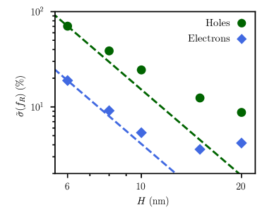
The variability due to interface roughness is significantly larger in hole than in electron qubits (also see Fig. 5). For the Larmor frequencies, this results from the dependence of the -factors of holes on the confinement discussed above. For the Rabi frequencies, this mostly results from the different electron and hole effective masses. Indeed, the in-plane mass of electrons and holes are similar (), but the confinement mass are different: for electrons and for heavy holes. According to Eq. (5), the interface roughness has, therefore, stronger impact on the hole than on the electron qubits when (vertical confinement dominated by the structure). This may not be the case, however, in thicker channels operating in the limit (vertical confinement dominated by the electric field).
IV Charge traps
IV.1 Holes
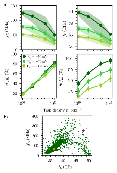
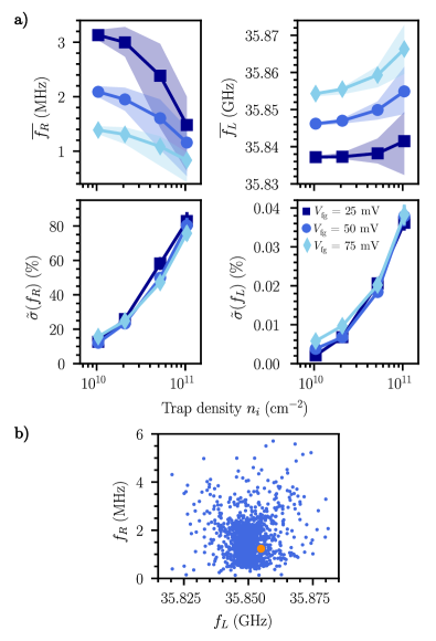
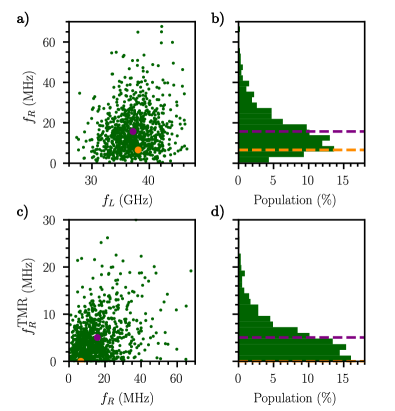
The average Rabi frequency , the average Larmor frequency , and the RSDs and of the hole qubits are plotted as a function of the density of charge traps in Fig. 6a. The distribution of the Larmor and Rabi frequencies of the qubits is plotted in Fig. 6b for cm-2 and mV. Each point represents a particular realization of 5 unit charges in the whole device of Fig. 1a. The reference data and for the pristine device have been recomputed with a homogeneous density of charges at the Si/SiO2 interface (in order to capture the average electrostatic effect of the defects), and do therefore differ from those for interface roughness.
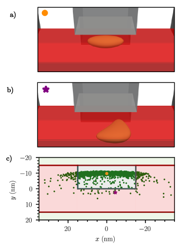
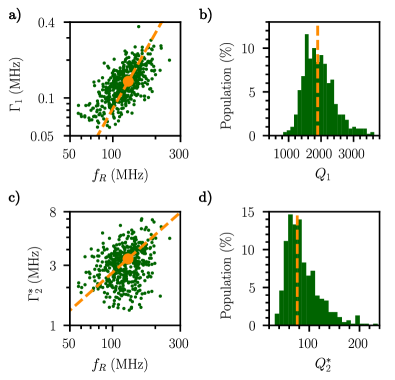
The data are much scattered, the Rabi frequency spanning, in particular, more than one order of magnitude. The distribution of Rabi frequencies is non-normal at large , so that we have added the first and third quartiles of this distribution on Fig. 6a as an extra measure of the variability (25% of the devices lie below, 25% above, and 50% within the shaded areas). There are also a few strong outliers with Rabi frequencies MHz that were removed from the statistics.666We have actually removed from the statistics strong outliers with Rabi frequencies greater than . They usually result from the resonance between two coupled dots and are extremely sensitive to the bias point. The envelope functions are, indeed, strongly shifted and distorted by the disorder, especially along the channel (the weakest confinement axis), as illustrated in Fig. 7c. These real-space distortions give rise to large fluctuations of and owing to the strong spin-orbit coupling in the valence band. The displacements of the dots along the channel will also complicate the management of the exchange interactions between neighboring dots.
Remarkably, and in contrast with interface roughness, the charge traps directly modulate the lateral (rather than vertical) confinement, because the hole gets excluded from the whole thickness of the film in the vicinity of a defect ( Å at cm-2 and meV, while Å on Fig. 4b). As a consequence, and remain good principal axes of the -tensor, so that shows significant correlations with despite partial cancellations between the variations of and (Fig. 8). The deviations of the Larmor and Rabi frequencies are, therefore, both primarily dependent on and are broadly correlated (Fig. 6). In general, the charge traps, which repel the holes, squeeze the dots and hinder their motion, so that the average Rabi frequency decreases with increasing . As a matter of fact, nm on Fig. 8, which is smaller than nm in the pristine, traps-free device (table 1), but larger than nm in the reference device with a homogeneous distribution of charges at the Si/SiO2 interface (orange point in Figs. 6–8). In the same way, the average MHz is larger than the Rabi frequency MHz in that reference device, which outlines the non-linear response of the spins to nearby traps (they are indeed expected equal in a first-order perturbation theory such as Appendix C). The highest Rabi frequencies typically result from the the formation of strongly coupled multiple dots below the gate, allowing for large charge oscillations under electrical driving.
decreases with decreasing , but remains significant down to cm-2 (only one charge trap in the whole device of Fig. 1a). Indeed, a single stray defect can have a sizable effect of the nearby qubit(s), as shown in Appendix E. As discussed in Appendix C, the scattering strength of the charged traps is expected to scale as within first-order perturbation theory; actually increases faster than , but slower than . This is presumably due to the facts that also decreases with increasing , and that is dominated by the defects very near or in the dot, to which the response is non linear. tends to saturate at large due to a complex interplay between the variations of the -factors and of the strongly distorted dots.
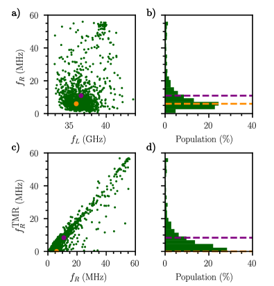
IV.2 Electrons
The data for electrons are shown in Fig. 9. We remind that defects are amphoteric, and therefore repel electrons in -type devices (as they do repel holes in -type devices) once charged. The variability of the Larmor frequency is much smaller for electrons than for holes for the same reasons as for interface roughness (weak dependence of on vertical confinement). The average Larmor frequency slightly increases with increasing as the electron tends to move upward in the channel (the charged defects being less screened by the gate on the bottom than on the top interface). The variability of the Rabi frequency is, nonetheless, as large as for holes, especially at the highest trap densities. The potential of the charge traps is, indeed, the same for electrons and holes, in contrast with the effective potential for interface roughness, which depends on the confinement mass of the carriers [Eq. (5)]. Also, this potential is expected to have similar effects on the in-plane motion of electrons and holes, since the in-plane mass of both carriers is comparable.777In fact, the charge traps have a stronger effect on the in-plane motion of holes (larger ) owing to the multi-bands character of the Hamiltonian. Yet the scaling of the Rabi frequency is softer for holes () than for electrons (). Therefore, the net impact of charged traps is about the same for electrons and holes. The Rabi frequency of electrons remains largely correlated to , except for some specific trap configurations where the dot is strongly displaced or squeezed, or, on the opposite, where coupled dots form under the gate as a result of the disorder.
The charge disorder variability of the Larmor and Rabi frequencies of both electron and hole qubits shows only a weak dependence on the channel thickness .
V Discussions
We now outline the implications of the above results and possible strategies to mitigate disorder. We discuss, in particular, the relations between the variability of the Rabi frequencies and of the qubit lifetimes (, ), and the consequences for multi-qubit systems.
V.1 Sensitivity to disorder
Spin-orbit qubits are sensitive to disorder. This is the price to pay for the possibility to manipulate the spins electrically. Unless material and device engineering can mitigate the disorder, each individual qubit needs to be characterized separately in order to account for its own “personality”. On the other hand, the same spin-electric coupling provides opportunities to tune the qubits and partly correct for device-to-device deviations. This, of course, requires that the spread of characteristics is manageable, and that the qubits remain functional and can be coupled together.
In this respect, charge traps are much more critical than interface roughness. This is reminiscent of the behavior of classical field effect transistors. Indeed, a spin qubit at a Si/SiO2 interface is in essence a field-effect transistor operating in the low electric field/low carrier density range; the carrier mobility is well known to be primarily limited by the (unscreened) Coulomb disorder in this regime.Esseni et al. (2003); Niquet et al. (2014); Nguyen et al. (2014) Disorder is an even stronger concern for qubits as the relevant energy scales are typically in the sub-meV range (as compared to the or source-drain voltage range for classical transport) while fluctuations are in the few meV range.
We would like to draw attention to the fact that electron spin qubits are subject to additional sources of variability not accounted for in this work. First, spin-valley-orbit coupling (SVOC) is neglected in the present effective mass approximation. Interface roughness is known to be responsible for a significant variability of the valley splitting and spin-valley mixing, as discussed for example in Refs. Culcer et al., 2010; Bourdet and Niquet, 2018. This is not expected to have a strong impact on the Rabi frequencies (the dipole matrix elements between valley states being small along the main direction of the EDSR motion), unless the valley and Zeeman splittings are close enough to allow for intrinsic SVOC-driven Rabi oscillations.Corna et al. (2018); Bourdet and Niquet (2018) However, SVOC may slightly lower the -factor of electrons (by up to a few hundredths);Veldhorst et al. (2015b); Ruskov et al. (2018); Ferdous Rifat et al. (2018); Tanttu et al. (2019) device to device fluctuations of the -factor would give rise to variations of the Larmor frequency MHz at a net field T. Such fluctuations are on the scale or even larger than those reported in Figs. 3 and 9. Achieving robust and controllable valley splitting is actually a key to the realization of well defined two-level systems for spin manipulation and readout. Also, the electron spin qubits may be sensitive to local inhomogeneities (roughness, variations of the magnetic polarization…) and global misalignment (misplacement/misorientation) of the micro-magnets.Yoneda et al. (2015); Simion et al. (2020) These disorders, which are specific of extrinsic spin-orbit coupling, are addressed in Appendix D.
As pointed out in section II, we may attempt to drive the hole devices with the two side gates on the left and right of the dot (the present micro-magnets layout is not suitable for that purpose in the electron qubits). The dot then essentially moves as a whole along the channel axis . As discussed in Ref. Michal et al., 2021, the Rabi frequency in this “iso-Zeeman” mode is proportional to . The situation is not, therefore, expected to be more favourable: the channel axis being typically the direction of weakest confinement, shows strong device-to-device variations (as evidenced in Figs. 4 and 7). This conclusion is supported by numerical simulations showing comparable or even larger Rabi frequency variability in this driving mode (see Appendix E). As a matter of fact, these simulations also show the emergence of a significant -TMR contribution on top of the original iso-Zeeman one, the disorder giving rise to sizable modulations of the gyromagnetic factors under driving.
Finally, we would like to emphasize that the present data were collected at fixed gate voltage. We may, alternatively, collect data at fixed chemical potential in the dot (fixed ground-state energy), with the prospect of reducing the variability (because shall also correlate with the extension of the ground-state wave function). This is moreover closer to the experimental situation when the dots remain connected to reservoirs of particles while being operated. The computational procedure is, however, more complex and time-consuming, as the bias must be corrected for each disordered device in order to achieve the target chemical potential. Yet our attempts for interface roughness and charge traps did not show any clear improvement of the variability. As a matter of fact, even in a separable 3D model, working at fixed chemical potential does not ensure that the , , motion energies are all preserved (only their sum is). As suggested above, the variability can indeed be partly compensated by bias adjustments, however aimed at correcting, e.g., the extension along or the position along , and not the total energy of the dot. Such bias corrections may nonetheless be limited by the stability diagram of the devices. To be more specific, the Larmor frequency of 46% of the rough hole qubits, and of 55% of the hole quits with charged traps can be matched to the pristine device with bias corrections mV ( mV; nm, nm; cm-2). This mV is however already about twice the typical charging energy and therefore calls for tight control over the barriers to prevent inter-dot tunneling. The situation is not much better for electrons despite the smaller variability of the Larmor frequency, as the Stark effect (electrical tunability of ) is much weaker than for holes.
V.2 Relations with qubit lifetimes
The disorder will also give rise to variability in the qubit relaxation time and dephasing time . This can have detrimental consequences on the performances of a multi-qubits processor.
First, we expect as a general trend that the devices with the largest Rabi frequencies also show the shortest relaxation times . Indeed, in the Fermi-Golden rule/Bloch-Redfield approximation, where the exponent depends on the relaxation mechanism ( for Johnson-Nyquist noise, to for phononsPaladino et al. (2014); Tahan and Joynt (2014); Huang and Hu (2014); Li et al. (2020)), and is the matrix element of an operator that describes some spin-electric coupling. can, therefore, be expected to scale with (which is also such a transverse spin-electric coupling matrix element).
The pure dephasing rate is, likewise, , where for some coupling operator , for regular noise (Bloch-Redfield approximation) and for quasi-static noise.Paladino et al. (2014) Although the relations between the longitudinal matrix elements involved in and the transverse matrix elements involved in and is far from obvious, we can still expect that devices with stronger spin-electric coupling show, on average, larger , , and , unless some sweet spot has been found. Some defects themselves may be a source of noise if their charge trapping/detrapping or structural rearrangement times are shorter than the duration of an experiment.de Sousa (2007) This problem goes, however, beyond the scope of the present work.
We illustrate these trends on the relaxation time and on the pure dephasing time of holes. The phonon-limited is calculated along the lines of Ref. Li et al., 2020. As for , we assume a quasi-static noise with finite bandwidth whose action on the qubit can be modeled as an effective fluctuation of the gate voltage with rms amplitude . Then,Dial et al. (2013)
| (9) |
where is the derivative of the total potential in the device with respect to the gate voltage . We set V as an illustration. Note that for such a noise the coherence decays as instead of .
The distribution of Rabi frequencies and relaxation rates is plotted in Fig. 10a for interface roughness disorder ( nm, nm). The corresponding data for are plotted in Fig. 10c. They were computed at T along ( scalesLi et al. (2020) as and as ). As hinted above, the larger the Rabi frequency, the larger (and, to a much lesser extent, ) tends to be. There is, nonetheless, a significant spread of the single qubit quality factors and (number of rotations that can be achieved within or ), as shown in Fig. 10b, d.
In an ensemble of qubits, the relevant figure of merit for relaxation is however . It is limited by the slowest and by the shortest-lived qubits, which are in principle different. Assuming , we can give an estimate for :
| (10) |
where is the quality factor of the pristine device. A similar expression can be obtained for , with a possibly different . This highlights how detrimental the variability can be for the operation of an ensemble of qubits. In the case of Fig. 10, on the 90% best qubits (450 best individual out of 500 devices), and , much lower than and . The operation of slow qubits can be sped up by increasing the driving RF power ( at same power-corrected Rabi frequencies), yet at the expense of a more complex RF management on the chip, and at the risk of heating up the qubits.
V.3 Mitigation of the disorder
The qubits may be made more resilient to variability through material and/or device engineering. In particular, the previous sections highlight how critical is the quality of materials and interfaces for the control and reproducibility of spin qubits. Improving the smoothness and passivation of the Si/SiO2 interface will definitely reduce variability; a RSD however calls for very clean and stable interfaces with charged defect densities cm-2 that are at the state-of-the-art.
The interface roughness variability can be largely alleviated by a proper optimization of the channel/film thickness and vertical electric field in order to reach the best balance between single qubit performances and sensitivity to disorder (see Fig. 5). This optimum is presumably dependent on the device layout and mechanisms used to drive the spin.
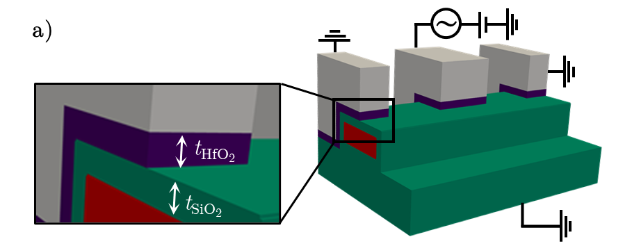
Nevertheless, one of the most reliable solutions to the variability problem is to switch from a crystalline/amorphous interface such as Si/SiO2 to an epitaxial interface such as Si/SiGe (electron qubits) or Ge/SiGe (hole qubits). Indeed, epitaxial interfaces show, in principle, low roughness and very small density of traps. Strains must be carefully addressed in order to avoid threading dislocations in the active areas, but this is now fluently managed in group IV materials. The four hole qubits device of Ref. Hendrickx et al., 2021 was actually realized in a Ge/SiGe quantum well controlled by accumulation gates.
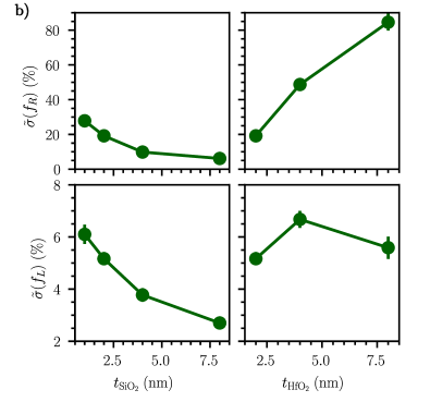
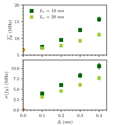
The charged defects are then deported at the surface of the heterostructures on which the metal gates are deposited. This surface is usually no more than 50 nm away from the well (in order to keep a tight enough electrostatic control on the qubits). We emphasize, though, that the impact of charge traps decreases significantly once they are taken away from the quantum dots. As an illustration, we have considered SOI hole devices with a SiO2/HfO2 gate stack (Fig. 11a). The channel is therefore now separated from the gate by a layer of SiO2 with thickness , and by a layer of HfO2 with thickness (). This HfO2 layer only extends below the gates and not under the spacers. We then introduce the charged defects at the SiO2/HfO2 instead of the Si/SiO2 interface, with density cm-2 only chosen888We emphasize that the SiO2/HfO2 interface is known to be a strong source of Coulomb scattering in classical CMOS devices,Zeng et al. (2017b) with apparent charge densities reaching cm-2. This test system is introduced to illustrate trends in a device similar to section IV, and is not meant to give a realistic account of disorder at the SiO2/HfO2 interfaces, which shall preferably be avoided in qubit devices. for illustrative purposes.Zeng et al. (2017b) The RSDs and of the Larmor and Rabi frequencies are plotted as a function of and in Fig. 11b. The variability decreases when the SiO2 is made thicker and the traps are moved away from the channel. Remarkably, the variability increases rapidly with the thickness of the HfO2 layer because the screening of the charge traps by the metal gate is softened.Zeng et al. (2017b) In general, surrounding the qubits by materials with higher dielectric constant (SiGe SiO2), and by a dense set of gates will reduce the impact of charged defects on variability (and possibly of charge noise on qubit lifetimes).999This “electrostatic” argument assumes that these materials are not themselves sources of additional static or dynamic noise. Working in the many electrons/holes regime may also enhance screening, but usually makes the dots larger and more responsive to disorder. The optimal number of particles in the dots (as far as variability is concerned) remains, therefore, an open question.Leon et al. (2020)
Finally, the model of Appendix C shows that the variability increases with the in-plane mass (at given dot sizes and ). Heavier particles indeed localize more efficiently in the disorder. It is, therefore, a priori advantageous to switch from silicon to lighter mass materials such as germanium for holes (for interface roughness, the variability is when so that Ge is advantageous over Si even in this regime). However, the dots are usually made larger in light mass materials (the dot sizes and scale as in a given parabolic potential for example, and as at given confinement energy), hence can be more polarizable and sensitive to disorder. Eq. (39) actually suggests that the variability may not necessarily improve when decreasing the mass at given confinement energy, especially in the presence of long-wavelength disorders such as charge traps.
VI Conclusions
We have investigated the variability of single qubit properties (Larmor and Rabi frequencies) due to disorder at the Si/SiO2 interface (roughness and charge traps) in MOS-like devices. We have, in particular, compared hole qubits subject to intrinsic spin-orbit coupling and electron qubits subject to a synthetic spin-orbit coupling created by micro-magnets. The Larmor frequencies of electrons are more robust to disorder than the Larmor frequencies of holes, which are rather sensitive to changes in the potential landscape. The Rabi frequencies show anyway much larger variability than the Larmor frequencies for both kinds of carriers. The deviations of the Rabi frequencies can be traced back to the modulations of the size of the dots by the disorder. In thin films, holes are more sensitive to interface roughness than electrons because the confinement mass of the heavy-holes is smaller than the confinement mass of the electrons in the Z-valleys (hence the effects of fluctuations of the film thickness are larger). The main source of variability is, however, charge traps at the Si/SiO2 interface, which can spread both electron and hole Rabi frequencies over one order of magnitude. The dots can be significantly distorted and displaced by charge disorder, which does not only scatter one qubit properties, but may also complicate the management of exchange interactions between the dots. The disorder also scatters the relaxation and dephasing times, which systematically degrades the figures of merit of an ensemble of qubits (as the lifetimes of such an ensemble are limited by the poorest qubits). Low variability calls for smooth and clean interfaces with charge traps densities cm-2. This is presumably more easily achieved with epitaxial heterostructures such as Si/SiGe or Ge/SiGe, where the residual (surface) charge traps can be deported tens of nanometers away from the active layer. The impact of charge traps indeed decreases very fast once they are moved away from the qubits, especially when the latter are embedded in materials with high dielectric constants and are controlled by dense sets of gates that screen the Coulomb disorder.
Acknowledgements
We thank Michele Filippone for fruitful comments and suggestions. This project was supported by the European Union’s Horizon 2020 research and innovation programme under grant agreement 951852 (project QLSI), and by the French national research agency (project MAQSi).
Appendix A Vector potential created by the micro-magnets
The magnetic field created by micro-magnets has been discussed, for example, in Refs. Neumann and Schreiber, 2015, Yang et al., 1990, Goldman et al., 2000 and Yoneda et al., 2015. Here we deal with the calculation of the corresponding vector potential, which is the natural input for quantum mechanics codes (see appendix B).
We consider a micro-magnet layout that can be viewed as an arrangement of homogeneous bar magnets. The total vector potential and magnetic field are hence the sum of those of each individual bar magnet. Let be a bar magnet with magnetic moment density and sides , and along three orthonormal axes , , and . The vector potential created at point by this magnet is:
| (11) |
Setting in the axis set with the origin at the center of the magnet, explicit integration yields:
| (12) |
where and is the magnetic polarization. The functions are:
| (13a) | ||||
| (13b) | ||||
| (13c) | ||||
with . The components of the magnetic field then read:
| (14) |
with:
| (15a) | ||||
| (15b) | ||||
| (15c) | ||||
The above expressions for the vector potential and magnetic field are valid outside the magnet.
In the present calculations, and we assume that the magnetic polarizationNeumann and Schreiber (2015) of Cobalt T is saturated in an external magnetic field T along . The total vector potential is the sum of the vector potentials and of the two micro-magnets, and of the vector potential of the external magnetic field.
Appendix B Rabi frequency in a gradient of magnetic field
We compute the Rabi frequencies of the electrons with an anisotropic effective mass model for the valleys. We make the substitution (with the wave vector) and add the spin Zeeman Hamiltonian:
| (16) |
where , is Bohr’s magneton and is the vector of Pauli matrices. We next compute the energies and the wave functions of the the ground-state and first excited state in the electrostatic potential of the gates with a finite-differences method. When a time-dependent modulation is applied to the front gate, resonant with the Zeeman splitting , the spin rotates at Rabi frequency:Bourdet and Niquet (2018); Venitucci et al. (2018)
| (17) |
where is the derivative of the electrostatic potential in the device with respect to the front gate voltage (the potential created by a unit potential on that gate while all others are grounded when the electrostatics is linear, as is the case here).
When the gradient of magnetic field is homogeneous enough, we can derive an alternative formulation for the Rabi frequency that emphasizes its dependence on the electric dipole of the dot. We hence assume that the magnetic field created by the micro-magnets can be approximated near the dot as:
| (18) |
where is some reference point and is the matrix of derivatives of the magnetic field components ():
| (19) |
Note that the ’s are not independent as they must fulfill Maxwell’s equations and outside the magnets, namely:
| (20a) | |||
| (20b) | |||
Neglecting the action of the vector potential on the orbital motion, the effective Hamiltonian of the spin can then be written:
| (21) |
Here, is the average position of the dot in the ground-state at zero magnetic field, is the average micro-magnet field seen by the dot, and is the time-dependent modulation of the gate voltage that drives the spin. When is resonant with the Zeemann splitting , the spin rotates at Rabi frequency:
| (22) |
where is the unit vector aligned with the total magnetic field . The derivation is similar to the -matrix formula for intrinsic spin-orbit coupling.Venitucci et al. (2018)
The response can be evaluated using either perturbation theoryPioro-Ladrière et al. (2008) or finite differences at two biases and :
| (23) |
Although the above estimation is not necessarily much faster than Eq. (17) for a single orientation of the magnetic field , it clearly highlights the relation between the Rabi frequency and the electrical response of the dot. In the present devices, and the matrix read at the average position of the pristine dot ( mV):
| (24a) | ||||
| (24b) | ||||
Therefore,
| (25) |
because the dot essentially moves along when driven by the central gate.
Appendix C Simple model for the variability of the Rabi frequency of electrons
According to Appendix B, the Rabi frequency of electrons is in the present setup. In this appendix, we derive a simple model for the variability of in a disordered dot using first-order perturbation theory.
We consider a quantum dot with energies and eigenstates at zero magnetic field (we discard, therefore, the spin index for simplicity). In the presence of a disorder potential , the first-order ground state reads:
| (26) |
so that:
| (27) |
We have assumed real wave functions (as always possible at zero magnetic field in the absence of spin-orbit coupling). Next,
| (28) |
where stands for . Moreover,
| (29a) | ||||
| (29b) | ||||
where, as before, is the derivative of the electrostatic potential in the device with respect to the front gate voltage .
This problem can be solved analytically in some paradigmatic cases. We assume that the motions along , , are separable in the pristine dot, and that the confinement along is harmonic, with characteristic energy . We also assume that the gate creates a homogeneous electric field along , that is with some characteristic device length. Then, using the relation
| (30) |
for the eigenstates of the harmonic oscillator, we get:
| (31) |
where:
| (32) |
and:
| (33) |
Here and are the wave functions with respectively one and two quanta of excitation along . Therefore, if , the average Rabi frequency is that of the pristine device, and:
| (34) |
where:
| (35) |
with the auto-correlation function of the disorder (assumed independent on ). We next introduce the Fourier transform of (the power spectrum of the disorder):
| (36) |
and reach:
| (37) |
We now apply this expression to interface roughness disorder in a thin film with thickness . When , the disorder potential is given by Eq. (5), and the auto-correlation function is twice Eq. (1) (because there are two independent top and bottom interfaces). Since depends only on , we just need to specify the wave function in that plane, and to integrate Eq. (37) over [. Therefore, we also assume parabolic confinement along , with a possibly different characteristic energy , so that:
| (38) |
where and are the characteristic sizes of the pristine dot. Substituting the Fourier transforms of Eqs. (1) and (38) into Eq. (37), we finally reach:
| (39) |
This expression highlights several key points discussed in this work:
- •
-
•
The variability has a non-monotonous behavior with , and shows a peak at:
(40a) (40b) (40c) As discussed in section III, fluctuations with wave lengths are averaged out, while the interface becomes flat again on the scale of the dot when . The fluctuations with wave lengths comparable to the size of the dot are actually the most detrimental to the variability.
-
•
At given dot sizes and , the variability is proportional to the in-plane mass : the heavier the particles, the stronger they localize in the disorder. We emphasize nonetheless that and also depend on for a given confinement potential.
-
•
When increasing the dot size or , the dot becomes more polarizable and responsive to the disorder. Yet fluctuations along the driving axis are expected to have much more impact on the motion of the dot than fluctuations along the transverse axis . Actually, even decreases monotonously with increasing , because the fluctuations get better averaged out on the scale of the dot. However, increases monotonously with increasing ; it scales as when , and as when . The relative variability decays slower than the absolute variability when because also tends to 0 as .
We point out that the expression of as a function of , and is distinctive of the confinement potential (e.g., parabolic triangular), of the operators coupling the spin and electric fields (e.g., for electrons and for holes), and on the power spectrum of the disorder. In the devices investigated in this work, the dots are confined in an anharmonic potential along , and show weaker scalings with (see Fig. 2) than expected from Eq. (39), especially for holes.
Finally, we briefly discuss the dependence of the variability of on the density of defects at the Si/SiO2 interface. As a prototypical example, we consider an ensemble of defects at random positions on a planar interface with area located at . We assume that the vertical confinement at this interface is strong enough that we can introduce an effective 2D potential for a point charge at position (the defect potential averaged over the ground-state envelope function along ). We also assume that the interface is homogeneous, so that only depends on .101010We emphasize that decays typically faster than due to the presence of metal gates in the device. Then, the total disorder potential reads:
| (41) |
If the are uncorrelated, we reach when :Niquet et al. (2014)
| (42a) | ||||
| (42b) | ||||
where:
| (43) |
and:
| (44) |
is the spatial auto-correlation function of the potential of a single charge. is the potential created by a homogeneous density of traps at the interface that simply shifts the dot energies, while only gives rise to variability. Therefore, is expected to scale as according to Eq. (37). Indeed, two defects would scatter Rabi frequencies twice as much as a single defect only if they were systematically at the same positions.
The data of Figs. 6 and 9 scale faster than but slower than . We attribute this discrepancy to the breakdown of the above assumptions. In particular, the average Rabi frequency decreases with increasing in the non-parabolic confinement potential of the 1D channel, which strengthen the scaling of . Also, the variability is dominated by the defects that are close to or within the dot, and whose effects go beyond first-order perturbation theory. At small densities, the likelihood to have a defect within the dot directly scales as .
Appendix D Effects of micro-magnet imperfections
In this Appendix, we briefly discuss the effects of disorder in the micro-magnets on the variability of electron spin qubits. The relevant parameters of the micro-magnets are displayed in Fig. 12a.
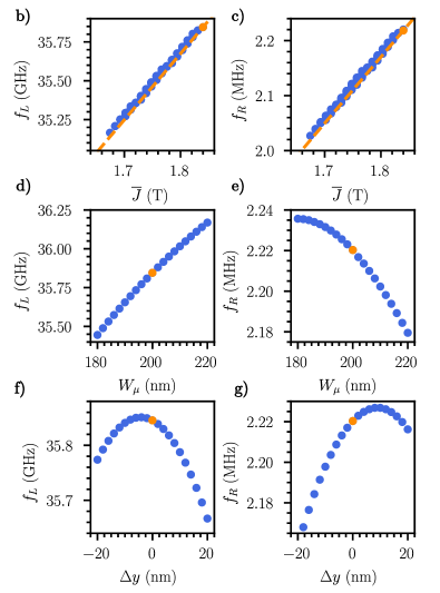
The qubits may be sensitive to local inhomogeneities of the magnets (roughness, variations of the magnetic polarization ), and to “global” (but more systematic) deficiencies such as misalignment (misplacement and misorientation).Yoneda et al. (2015); Simion et al. (2020) The roughness of the magnets tends to be softened in the far field and is likely not a strong concern, unless particularly large or long-ranged. The variations of the magnetic polarization due to material inhomogeneity or incomplete saturation can be readily addressed when they take place over length scales much longer than the distance to the qubits (that is, in the hundreds of nm range). The magnetic polarization can then be considered as locally homogeneous, but device dependent. The Larmor and Rabi frequencies of the pristine qubit are thus plotted in Figs. 12b,c as a function of the average magnetic polarisation of the two magnets (they are almost independent on in this range). The Rabi frequency being directly proportional to the gradient of the micro-magnets field, any relative variation of results in a similar relative variation of (dotted lined in Fig. 12c). The Larmor frequency shows a weaker, yet significant linear dependence on as the micro-magnets field is only of the the total magnetic field (dotted lined in Fig. 12b). As a matter of fact, a variation of results in a 100 MHz drift of the Larmor frequency, which is sizable with respect to the distributions shown in Figs. 3 and 9. The homogeneity of the magnets can, therefore, be critical for the control of the Larmor frequencies.
We have also plotted in Figs. 12d,e the Larmor and Rabi frequencies as a function of the width of the trench between the magnets (nominally nm). increases and decreases when widening the trench because increases (the qubit looks better aligned with the magnets) but decreases. Making a bevel trench is actually a solution to detune the qubits on purpose in order to address them individually at different Larmor frequencies ( MHz/nm).Yoneda et al. (2015) Finally, the Larmor and Rabi frequencies are plotted in Figs. 12f,g as a function of the misaligment between the channel and the micro-magnets trench. The variations are small and mostly second-order in the nm range because symmetric positions on both sides of the mirror plane of the magnets are roughly (but not strictly) equivalent (the major component is the same but the minor component changes sign). If the micro-magnets are misoriented by with respect to the channel axis, neighboring qubits (that are 60 nm apart in the design of Fig. 1) are shifted by nm.
Appendix E Additional figures
In this Appendix, we provide additional data on the effects of charge traps on the Larmor and Rabi frequencies of electron and hole qubits, and discuss some results on hole qubits driven in the iso-Zeeman EDSR mode.
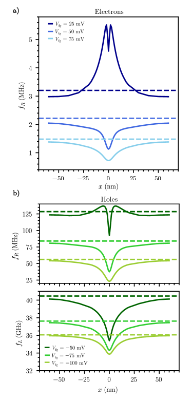
E.1 Effects of a single charge on electron and hole qubits
The Larmor and Rabi frequency of electron and hole qubits is plotted in Fig. 13 as a function of the position of a single charge along the channel. This charge is positive for hole qubits, negative for electron qubits, and is located on the top facet. The deviations from the pristine qubit are sizable when the charge is within nm from the qubit. Note the “overshoot” of the Rabi frequency at small bias when the charge goes through the gate and tends to split the dot in two strongly coupled pieces.
E.2 Hole qubits driven in the iso-Zeeman EDSR mode
We now consider a hole qubit driven by a RF field on the left gate and on the right gate. This field shakes the dot as a whole in the quasi-harmonic confinement potential along the channel axis; the principal -factors are therefore little dependent on the position of the hole (no -TMR in the pristine device). The dot however experiences Rashba-type spin-orbit interactions that rotate the spin.Kloeffel et al. (2011, 2018); Michal et al. (2021) The magnetic field is oriented along , which is closer to the optimum in this configuration.
At variance with the -TMR mode, the Rabi frequency of the pristine device increases with increasingly negative because the Rashba spin-orbit coupling gets enhanced by the lateral and vertical electric fields. It reaches MHz at mV (where it is almost saturated).111111The static bias on the left and right gates is set to meV in order not to impede the motion of the dot by a stiff confinement along . It is much smaller than the -TMR Rabi frequency because -tensor modulation is more efficient than Rashba spin-orbit interactions over a wide range of bias voltages in such heavy-hole devices.Michal et al. (2021) Moreover, the left and right gates are pretty far from the qubit in the present layout (and are partly screened by the front gate), which can be however compensated by a larger drive amplitude.
The distribution of Larmor and Rabi frequencies for interface roughness ( nm, nm) and charge traps ( cm-2) are plotted in Figs. 14 and 15. The RSD for interface roughness and for charge traps are much larger than in the -TMR mode (respectively and ). Strikingly, the average Rabi frequency systematically increases in the presence of disorder. This results from the emergence of a strong -TMR contribution on top of the original iso-Zeeman mechanism in the disordered qubits (the gyromagnetic factors now depending significantly on the position of the dot along ). To support this conclusion, we have plotted the distribution of this -TMR contribution, calculated from the sole dependence of the principal -factors on the driving RF field, in Figs. 14 and 15. It is indeed zero in the pristine qubit, but can reach up to a few tens of MHz in the disordered devices. -TMR even becomes the prevalent mechanism in a significant fraction of the qubits in the presence of charge traps (as the wave function can be substantially distorted by the RF drive). The weak confinement along , necessary for efficient driving (the iso-Zeeman Rabi frequency scales as ),Michal et al. (2021) as well as the mixing with a strong, disorder-induced -TMR contribution explain the huge variability of the Rabi frequencies. The average Rabi frequency , and the absolute standard deviation are also plotted as a function of the rms interface roughness in Fig. 16. As expected, increases almost linearly with strengthening , while increases quadratically (since this increase is second order in the disorder when the latter averages to zero, as suggested by Appendix C). These trends were confirmed with atomistic tight-bindingBourdet and Niquet (2018) calculations on selected devices.
References
- Loss and DiVincenzo (1998) D. Loss and D. P. DiVincenzo, Physical Review A 57, 120 (1998).
- Hanson et al. (2007) R. Hanson, L. P. Kouwenhoven, J. R. Petta, S. Tarucha, and L. M. K. Vandersypen, Review of Modern Physics 79, 1217 (2007).
- Pla et al. (2012) J. J. Pla, K. Y. Tan, J. P. Dehollain, W. H. Lim, J. J. L. Morton, D. N. Jamieson, A. S. Dzurak, and A. Morello, Nature 489, 541 (2012).
- Zwanenburg et al. (2013) F. A. Zwanenburg, A. S. Dzurak, A. Morello, M. Y. Simmons, L. C. L. Hollenberg, G. Klimeck, S. Rogge, S. N. Coppersmith, and M. A. Eriksson, Review of Modern Physics 85, 961 (2013).
- Scappucci et al. (2020) G. Scappucci, C. Kloeffel, F. A. Zwanenburg, D. Loss, M. Myronov, J.-J. Zhang, S. De Franceschi, G. Katsaros, and M. Veldhorst, Nature Reviews Materials (2020), 10.1038/s41578-020-00262-z.
- Tyryshkin et al. (2012) A. M. Tyryshkin, S. Tojo, J. J. L. Morton, H. Riemann, N. V. Abrosimov, P. Becker, P. H. J., T. Schenkel, M. L. W. Thewalt, K. M. Itoh, and S. A. Lyon, Nature Materials 11, 143 (2012).
- Veldhorst et al. (2014) M. Veldhorst, J. C. C. Hwang, C. H. Yang, A. W. Leenstra, B. de Ronde, J. P. Dehollain, J. T. Muhonen, F. E. Hudson, K. M. Itoh, A. Morello, and A. S. Dzurak, Nature Nanotechnology 9, 981 (2014).
- Kawakami et al. (2014) E. Kawakami, P. Scarlino, D. R. Ward, F. R. Braakman, D. E. Savage, M. G. Lagally, M. Friesen, S. N. Coppersmith, M. A. Eriksson, and L. M. K. Vandersypen, Nature Nanotechnology 9, 666 (2014).
- Veldhorst et al. (2015a) M. Veldhorst, C. H. Yang, J. C. C. Hwang, W. Huang, J. P. Dehollain, J. T. Muhonen, S. Simmons, A. Laucht, F. E. Hudson, K. M. Itoh, A. Morello, and A. S. Dzurak, Nature 526, 410 (2015a).
- Kawakami et al. (2016) E. Kawakami, T. Jullien, P. Scarlino, D. R. Ward, D. E. Savage, M. G. Lagally, V. V. Dobrovitski, M. Friesen, S. N. Coppersmith, M. A. Eriksson, and L. M. K. Vandersypen, Proceedings of the National Academy of Sciences 113, 11738 (2016).
- Takeda et al. (2016) K. Takeda, J. Kamioka, T. Otsuka, J. Yoneda, T. Nakajima, M. R. Delbecq, S. Amaha, G. Allison, T. Kodera, S. Oda, and S. Tarucha, Science Advances 2, e1600694 (2016).
- Yoneda et al. (2018) J. Yoneda, K. Takeda, T. Otsuka, T. Nakajima, M. R. Delbecq, G. Allison, T. Honda, T. Kodera, S. Oda, Y. Hoshi, N. Usami, K. M. Itoh, and S. Tarucha, Nature Nanotechnology 13, 102 (2018).
- Watson et al. (2018) T. F. Watson, S. G. J. Philips, E. Kawakami, D. R. Ward, P. Scarlino, M. Veldhorst, D. E. Savage, M. G. Lagally, M. Friesen, S. N. Coppersmith, M. A. Eriksson, and L. M. K. Vandersypen, Nature 555, 633 (2018).
- Zajac et al. (2018) D. M. Zajac, A. J. Sigillito, M. Russ, F. Borjans, J. M. Taylor, G. Burkard, and J. R. Petta, Science 359, 439 (2018).
- Huang et al. (2019) W. Huang, C. H. Yang, K. W. Chan, T. Tanttu, B. Hensen, R. C. C. Leon, M. A. Fogarty, J. C. C. Hwang, F. E. Hudson, K. M. Itoh, A. Morello, A. Laucht, and A. S. Dzurak, Nature 569, 532 (2019).
- Xue et al. (2019) X. Xue, T. F. Watson, J. Helsen, D. R. Ward, D. E. Savage, M. G. Lagally, S. N. Coppersmith, M. A. Eriksson, S. Wehner, and L. M. K. Vandersypen, Physical Review X 9, 021011 (2019).
- Yang et al. (2020) C. H. Yang, R. C. C. Leon, J. C. C. Hwang, A. Saraiva, T. Tanttu, W. Huang, J. Camirand Lemyre, K. W. Chan, K. Y. Tan, F. E. Hudson, K. M. Itoh, A. Morello, M. Pioro-Ladrière, A. Laucht, and A. S. Dzurak, Nature 580, 350 (2020).
- Petit et al. (2020) L. Petit, H. G. J. Eenink, M. Russ, W. I. L. Lawrie, N. W. Hendrickx, S. G. J. Philips, J. S. Clarke, L. M. K. Vandersypen, and M. Veldhorst, Nature 580, 355 (2020).
- Hendrickx et al. (2021) N. W. Hendrickx, I. L. Lawrie William, M. Russ, F. van Riggelen, S. L. de Snoo, R. N. Schouten, A. Sammak, G. Scappucci, and M. Veldhorst, Nature 591, 580 (2021).
- Maurand et al. (2016) R. Maurand, X. Jehl, D. Kotekar-Patil, A. Corna, H. Bohuslavskyi, R. Laviéville, L. Hutin, S. Barraud, M. Vinet, M. Sanquer, and S. de Franceschi, Nature Communications 7, 13575 (2016).
- Crippa et al. (2018) A. Crippa, R. Maurand, L. Bourdet, D. Kotekar-Patil, A. Amisse, X. Jehl, M. Sanquer, R. Laviéville, H. Bohuslavskyi, L. Hutin, S. Barraud, M. Vinet, Y.-M. Niquet, and S. De Franceschi, Physical Review Letters 120, 137702 (2018).
- Watzinger et al. (2018) H. Watzinger, J. Kukučka, L. Vukušić, F. Gao, T. Wang, F. Schäffler, J.-J. Zhang, and G. Katsaros, Nature Communications 9, 3902 (2018).
- Hendrickx et al. (2020a) N. W. Hendrickx, D. P. Franke, A. Sammak, G. Scappucci, and M. Veldhorst, Nature 577, 487 (2020a).
- Hendrickx et al. (2020b) N. W. Hendrickx, W. I. L. Lawrie, L. Petit, A. Sammak, G. Scappucci, and M. Veldhorst, Nature Communications 11, 3478 (2020b).
- Camenzind et al. (2021) L. C. Camenzind, S. Geyer, A. Fuhrer, R. J. Warburton, D. M. Zumbühl, and A. V. Kuhlmann, “A spin qubit in a fin field-effect transistor,” (2021), arXiv:2103.07369 [cond-mat.mes-hall] .
- Winkler (2003) R. Winkler, Spin-orbit coupling in two-dimensional electron and hole systems (Springer, Berlin, 2003).
- Kloeffel et al. (2011) C. Kloeffel, M. Trif, and D. Loss, Physical Review B 84, 195314 (2011).
- Kloeffel et al. (2018) C. Kloeffel, M. J. Rančić, and D. Loss, Physical Review B 97, 235422 (2018).
- Li et al. (2020) J. Li, B. Venitucci, and Y.-M. Niquet, Physical Review B 102, 075415 (2020).
- Lawrie et al. (2020) W. I. L. Lawrie, N. W. Hendrickx, F. van Riggelen, M. Russ, L. Petit, A. Sammak, G. Scappucci, and M. Veldhorst, Nano Letters 20, 7237 (2020).
- Ciriano-Tejel et al. (2021) V. N. Ciriano-Tejel, M. A. Fogarty, S. Schaal, L. Hutin, B. Bertrand, L. Ibberson, M. F. Gonzalez-Zalba, J. Li, Y.-M. Niquet, M. Vinet, and J. J. L. Morton, PRX Quantum 2, 010353 (2021).
- Corna et al. (2018) A. Corna, L. Bourdet, R. Maurand, A. Crippa, D. Kotekar-Patil, H. Bohuslavskyi, R. Laviéville, L. Hutin, S. Barraud, X. Jehl, M. Vinet, S. De Franceschi, Y.-M. Niquet, and M. Sanquer, npj Quantum Information 4, 6 (2018).
- Rashba and Efros (2003) E. I. Rashba and A. L. Efros, Physical Review Letters 91, 126405 (2003).
- Golovach et al. (2006) V. N. Golovach, M. Borhani, and D. Loss, Physical Review B 74, 165319 (2006).
- Rashba (2008) E. I. Rashba, Physical Review B 78, 195302 (2008).
- Tokura et al. (2006) Y. Tokura, W. G. van der Wiel, T. Obata, and S. Tarucha, Physical Review Letters 96, 047202 (2006).
- Pioro-Ladrière et al. (2007) M. Pioro-Ladrière, Y. Tokura, T. Obata, T. Kubo, and S. Tarucha, Applied Physics Letters 90, 024105 (2007).
- Pioro-Ladrière et al. (2008) M. Pioro-Ladrière, T. Obata, Y. Tokura, Y.-S. Shin, T. Kubo, K. Yoshida, T. Taniyama, and S. Tarucha, Nature Physics 4, 776 (2008).
- Michal et al. (2021) V. P. Michal, B. Venitucci, and Y.-M. Niquet, Physical Review B 103, 045305 (2021).
- Zwerver et al. (2021) A. M. J. Zwerver, T. Krähenmann, T. F. Watson, L. Lampert, H. C. George, R. Pillarisetty, S. A. Bojarski, P. Amin, S. V. Amitonov, J. M. Boter, R. Caudillo, D. Corras-Serrano, J. P. Dehollain, G. Droulers, E. M. Henry, R. Kotlyar, M. Lodari, F. Luthi, D. J. Michalak, B. K. Mueller, S. Neyens, J. Roberts, N. Samkharadze, G. Zheng, O. K. Zietz, G. Scappucci, M. Veldhorst, L. M. K. Vandersypen, and J. S. Clarke, “Qubits made by advanced semiconductor manufacturing,” (2021), arXiv:2101.12650 [cond-mat.mes-hall] .
- Bernstein et al. (2006) K. Bernstein, D. J. Frank, A. E. Gattiker, W. Haensch, B. L. Ji, S. R. Nassif, E. J. Nowak, D. J. Pearson, and N. J. Rohrer, IBM Journal of Research and Development 50, 433 (2006).
- Roy et al. (2006) G. Roy, A. R. Brown, F. Adamu-Lema, S. Roy, and A. Asenov, IEEE Transactions on Electron Devices 53, 3063 (2006).
- Asenov et al. (2009) A. Asenov, A. R. Brown, G. Roy, B. Cheng, C. Alexander, C. Riddet, U. Kovac, A. Martinez, N. Seoane, and S. Roy, Journal of Computational Electronics 8, 349 (2009).
- Mezzomo et al. (2011) C. M. Mezzomo, A. Bajolet, A. Cathignol, R. Di Frenza, and G. Ghibaudo, IEEE Transactions on Electron Devices 58, 2235 (2011).
- Bourdet and Niquet (2018) L. Bourdet and Y.-M. Niquet, Physical Review B 97, 155433 (2018).
- Ibberson et al. (2018) D. J. Ibberson, L. Bourdet, J. C. Abadillo-Uriel, I. Ahmed, S. Barraud, M. J. Calderón, Y.-M. Niquet, and M. F. Gonzalez-Zalba, Applied Physics Letters 113, 053104 (2018).
- Wu and Guo (2020) T. Wu and J. Guo, IEEE Electron Device Letters 41, 1078 (2020).
- Simion et al. (2020) G. Simion, F. A. Mohiyaddin, R. Li, M. Shehata, N. I. Dumoulin Stuyck, A. Elsayed, F. Ciubotaru, S. Kubicek, J. Jussot, B. Chan, T. Ivanov, C. Godfrin, A. Spessot, P. Matagne, B. Govoreanu, and I. P. Radu, in 2020 IEEE International Electron Devices Meeting (IEDM) (2020) p. 30.2.1.
- Venitucci et al. (2018) B. Venitucci, L. Bourdet, D. Pouzada, and Y.-M. Niquet, Physical Review B 98, 155319 (2018).
- Note (1) The valence band edge energy is set to eV in hole qubits; likewise, the conduction edge energy is set to eV in electron qubits.
- Kato et al. (2003) Y. Kato, R. C. Myers, D. C. Driscoll, A. C. Gossard, J. Levy, and D. D. Awschalom, Science 299, 1201 (2003).
- Venitucci and Niquet (2019) B. Venitucci and Y.-M. Niquet, Physical Review B 99, 115317 (2019).
- Neumann and Schreiber (2015) R. Neumann and L. R. Schreiber, Journal of Applied Physics 117, 193903 (2015).
- Yang et al. (1990) Z. J. Yang, T. H. Johansen, H. Bratsberg, G. Helgesen, and A. T. Skjeltorp, Superconductor Science and Technology 3, 591 (1990).
- Goldman et al. (2000) J. R. Goldman, T. D. Ladd, F. Yamaguchi, and Y. Yamamoto, Applied Physics A 71, 11 (2000).
- Culcer et al. (2010) D. Culcer, X. Hu, and S. Das Sarma, Physical Review B 82, 205315 (2010).
- Jiang et al. (2012) Z. Jiang, N. Kharche, T. Boykin, and G. Klimeck, Applied Physics Letters 100, 103502 (2012).
- Abadillo-Uriel et al. (2018) J. C. Abadillo-Uriel, B. Thorgrimsson, D. Kim, L. W. Smith, C. B. Simmons, D. R. Ward, R. H. Foote, J. Corrigan, D. E. Savage, M. G. Lagally, M. J. Calderón, S. N. Coppersmith, M. A. Eriksson, and M. Friesen, Physical Review B 98, 165438 (2018).
- Tariq and Hu (2019) B. Tariq and X. Hu, Physical Review B 100, 125309 (2019).
- Hosseinkhani and Burkard (2020) A. Hosseinkhani and G. Burkard, Physical Review Research 2, 043180 (2020).
- Goodnick et al. (1985) S. M. Goodnick, D. K. Ferry, C. W. Wilmsen, Z. Liliental, D. Fathy, and O. L. Krivanek, Physical Review B 32, 8171 (1985).
- Niquet et al. (2014) Y.-M. Niquet, V.-H. Nguyen, F. Triozon, I. Duchemin, O. Nier, and D. Rideau, Journal of Applied Physics 115, 054512 (2014).
- Pirovano et al. (2000) A. Pirovano, A. Lacaita, G. Ghidini, and G. Tallarida, IEEE Electron Device Letters 21, 34 (2000).
- Esseni et al. (2003) D. Esseni, A. Abramo, L. Selmi, and E. Sangiorgi, IEEE Transactions on Electron Devices 50, 2445 (2003).
- Nguyen et al. (2014) V.-H. Nguyen, Y.-M. Niquet, F. Triozon, I. Duchemin, O. Nier, and D. Rideau, IEEE Transactions on Electron Devices 61, 3096 (2014).
- Bourdet et al. (2016) L. Bourdet, J. Li, J. Pelloux-Prayer, F. Triozon, M. Cassé, S. Barraud, S. Martinie, D. Rideau, and Y.-M. Niquet, Journal of Applied Physics 119, 084503 (2016).
- Zeng et al. (2017a) Z. Zeng, F. Triozon, S. Barraud, and Y.-M. Niquet, IEEE Transactions on Electron Devices 64, 2485 (2017a).
- Poindexter et al. (1984) E. H. Poindexter, G. J. Gerardi, M. Rueckel, P. J. Caplan, N. M. Johnson, and D. K. Biegelsen, Journal of Applied Physics 56, 2844 (1984).
- Gerardi et al. (1986) G. J. Gerardi, E. H. Poindexter, P. J. Caplan, and N. M. Johnson, Applied Physics Letters 49, 348 (1986).
- Poindexter (1989) E. H. Poindexter, Semiconductor Science and Technology 4, 961 (1989).
- Helms and Poindexter (1994) C. R. Helms and E. H. Poindexter, Reports on Progress in Physics 57, 791 (1994).
- Thoan et al. (2011) N. H. Thoan, K. Keunen, V. V. Afanas’ev, and A. Stesmans, Journal of Applied Physics 109, 013710 (2011).
- Bauza (2002) D. Bauza, IEEE Electron Device Letters 23, 658 (2002).
- Brunet et al. (2009) L. Brunet, X. Garros, F. Andrieu, G. Reimbold, E. Vincent, A. Bravaix, and F. Boulanger, in 2009 IEEE International SOI Conference (2009) p. 1.
- Pirro et al. (2016) L. Pirro, I. Ionica, G. Ghibaudo, X. Mescot, L. Faraone, and S. Cristoloveanu, Journal of Applied Physics 119, 175702 (2016).
- Vermeer et al. (2021) M. L. Vermeer, R. J. E. Hueting, L. Pirro, J. Hoentschel, and J. Schmitz, IEEE Transactions on Electron Devices 68, 497 (2021).
- Note (2) We model one device at a time, with a different seed for the random number generator used by the geometry builder.
- Note (3) The factor (instead of ) on the denominator of Eq. (2b) follows from the definition of the “unbiased” estimate of the variance. This so-called Bessel correction does not make significant differences given the large data sets considered here ().
- Davison and Hinkley (1997) A. C. Davison and D. V. Hinkley, Bootstrap Methods and their Application, Cambridge Series in Statistical and Probabilistic Mathematics (Cambridge University Press, 1997).
- Yoneda et al. (2015) J. Yoneda, T. Otsuka, T. Takakura, M. Pioro-Ladrière, R. Brunner, H. Lu, T. Nakajima, T. Obata, A. Noiri, C. J. Palmstrom, A. C. Gossard, and S. Tarucha, Applied Physics Express 8, 084401 (2015).
- Sakaki et al. (1987) H. Sakaki, T. Noda, K. Hirakawa, M. Tanaka, and T. Matsusue, Applied Physics Letters 51, 1934 (1987).
- Uchida and Takagi (2003) K. Uchida and S. Takagi, Applied Physics Letters 82, 2916 (2003).
- Jin et al. (2007) S. Jin, M. V. Fischetti, and T.-W. Tang, IEEE Transactions on Electron Devices 54, 2191 (2007).
- Note (4) As a matter of fact, in a thin film with thickness . Since 95% of the thickness fluctuations lie within a range, and the electron/hole tends to localize in the thickest parts of the channel (), we expect nm, in agreement with Fig. 4.
- Note (5) In the pristine device, , and are very good approximations to the principal axes of the -matrix.Venitucci et al. (2018) In disordered devices, the channel axis remains, in general, a good principal axis; yet in the presence of interface roughness (but not charge traps), the two other principal axes can make an angle of up to degrees with and . This rotation results from the coupling between the in-plane and out-of-plane motions induced by the interface roughness. Although small, it has sizable effects on the distribution of Larmor frequencies.
- Note (6) We have actually removed from the statistics strong outliers with Rabi frequencies greater than . They usually result from the resonance between two coupled dots and are extremely sensitive to the bias point.
- Note (7) In fact, the charge traps have a stronger effect on the in-plane motion of holes (larger ) owing to the multi-bands character of the Hamiltonian. Yet the scaling of the Rabi frequency is softer for holes () than for electrons (). Therefore, the net impact of charged traps is about the same for electrons and holes.
- Veldhorst et al. (2015b) M. Veldhorst, R. Ruskov, C. H. Yang, J. C. C. Hwang, F. E. Hudson, M. E. Flatté, C. Tahan, K. M. Itoh, A. Morello, and A. S. Dzurak, Physical Review B 92, 201401 (2015b).
- Ruskov et al. (2018) R. Ruskov, M. Veldhorst, A. S. Dzurak, and C. Tahan, Physical Review B 98, 245424 (2018).
- Ferdous Rifat et al. (2018) Ferdous Rifat, Kawakami Erika, Scarlino Pasquale, Nowak Michał P., Ward D. R., Savage D. E., Lagally M. G., Coppersmith S. N., Friesen Mark, Eriksson Mark A., Vandersypen Lieven M. K., and Rahman Rajib, npj Quantum Information 4, 26 (2018).
- Tanttu et al. (2019) T. Tanttu, B. Hensen, K. W. Chan, C. H. Yang, W. W. Huang, M. Fogarty, F. Hudson, K. Itoh, D. Culcer, A. Laucht, A. Morello, and A. Dzurak, Physical Review X 9, 021028 (2019).
- Paladino et al. (2014) E. Paladino, Y. M. Galperin, G. Falci, and B. L. Altshuler, Review of Modern Physics 86, 361 (2014).
- Tahan and Joynt (2014) C. Tahan and R. Joynt, Physical Review B 89, 075302 (2014).
- Huang and Hu (2014) P. Huang and X. Hu, Physical Review B 90, 235315 (2014).
- de Sousa (2007) R. de Sousa, Physical Review B 76, 245306 (2007).
- Dial et al. (2013) O. E. Dial, M. D. Shulman, S. P. Harvey, H. Bluhm, V. Umansky, and A. Yacoby, Physical Review Letters 110, 146804 (2013).
- Note (8) We emphasize that the SiO2/HfO2 interface is known to be a strong source of Coulomb scattering in classical CMOS devices,Zeng et al. (2017b) with apparent charge densities reaching cm-2. This test system is introduced to illustrate trends in a device similar to section IV, and is not meant to give a realistic account of disorder at the SiO2/HfO2 interfaces, which shall preferably be avoided in qubit devices.
- Zeng et al. (2017b) Z. Zeng, F. Triozon, and Y.-M. Niquet, Journal of Applied Physics 121, 114503 (2017b).
- Note (9) This “electrostatic” argument assumes that these materials are not themselves sources of additional static or dynamic noise.
- Leon et al. (2020) R. C. C. Leon, C. H. Yang, J. C. C. Hwang, J. C. Lemyre, T. Tanttu, W. Huang, K. W. Chan, K. Y. Tan, F. E. Hudson, K. M. Itoh, A. Morello, A. Laucht, M. Pioro-Ladrière, A. Saraiva, and A. S. Dzurak, Nature Communications 11, 797 (2020).
- Note (10) We emphasize that decays typically faster than due to the presence of metal gates in the device.
- Note (11) The static bias on the left and right gates is set to meV in order not to impede the motion of the dot by a stiff confinement along .