Spin-orbit torque control of spin waves in a ferromagnetic waveguide
Abstract
Spin-orbit torque (SOT) created by a spin current injected into a ferromagnet by an adjacent heavy metal or topological insulator represents an efficient tool for the excitation and manipulation of spin waves. Here we report the micromagnetic simulations describing the influence of SOT on the propagation of spin waves in the nanostructure having voltage-controlled magnetic anisotropy (VCMA). The simulations show that two spin waves travelling in the opposite directions can be generated in the center of the waveguide via the modulation of VCMA induced by a microwave voltage locally applied to the nanolayer. The amplitudes of these waves exponentially decrease with the propagation distance with similar decay lengths of about 2.5 m. In the presence of a direct electric current injected into the film beneath the waveguide center, the decay lengths of two spin waves change in the opposite way owing to different directions of the electric currents flowing in the underlying halves of the layer. Remarkably, above a critical current density (about A m-2 at zero absolute temperature and A m-2 at room temperature), SOT provides the amplification of the spin wave propagating in one half of the waveguide and strongly accelerates the attenuation of the wave travelling in the other half. As a result, a long-distance spin-wave propagation takes place in a half of the waveguide only. Furthermore, by reversing the polarity of the dc voltage applied to the heavy-metal layer one can change the propagation region and switch the travel direction of the spin wave in the ferromagnetic waveguide. Thus, the nanostructure can be employed as an electrically controlled magnonic device converting the electrical input signal into a spin signal, which can be transmitted to one of two outputs of the device.
I Introduction
Generation and propagation of spin waves in magnetic nanostructures currently attract great attention because such waves can be employed for the development of energy-efficient nanodevices for information transmission and processing [1, 2, 3]. The traditional technique of spin-wave excitation uses a microwave magnetic field created by a microstrip antenna [4, 5, 6], but it suffers from relatively low conversion efficiency. During the last decade, novel excitation techniques have been proposed and developed, which utilize spin-polarized electric currents exerting spin-transfer torque on the magnetization [7, 8, 9], voltage-controlled magnetic anisotropy (VCMA) in ferromagnet-dielectric heterostructures [10], and spin-orbit torque (SOT) generated by a spin current injected into a ferromagnetic film by an adjacent heavy metal [11, 12]. The approaches based on SOT are especially promising, because they enable not only the excitation of spin waves but also a strong increase in their propagation length [13, 14, 15, 16, 17]. Such an increase results from partial compensation of magnetic damping by SOT, which is created at the ferromagnet boundary by an electric current flowing in the heavy metal or topological insulator with a strong spin-orbit interaction via the spin Hall effect [18].
The functioning of magnonic devices also requires efficient control and manipulation of propagating spin waves [19]. In a spin-wave (magnon) transistor, the flow of spin waves from source to drain is modulated by spin waves injected from the gate [20, 21]. A spin-wave multiplexer or demultiplexer operates by guiding spin waves into one arm of Y- or T-shaped structures with the aid of magnetic fields [22, 23, 24]. The dipolar interaction between the two laterally adjacent spin-wave waveguides makes it possible to develop a reconfigurable nanoscale spin-wave directional coupler, which can function as a multiplexer, tunable power splitter, or frequency separator [25]. Since SOT can strongly affect the damping of spin waves [26], it could be useful for their control and modulation as well.
In this work, we propose a spin-wave switch controlled by SOT created by a direct electric current flowing in a heavy-metal layer adjacent to a ferromagnetic waveguide. In such a device, two spin waves are excited at the center of the waveguide, which propagate in opposite directions and have similar decay lengths in the absence of SOT. In contrast, when sufficient non-uniform SOT is created by an electric current injected into the heavy-metal layer near the waveguide center, the propagation length of one of these waves strongly increases, whereas the other wave experiences a fast decay. We validate our proposal by micromagnetic simulations performed for the // heterostructure, where spin waves are generated electrically by an oscillating VCMA associated with the interface (Fig. 1). In particular, it is shown that, at zero absolute temperature, the critical current density providing complete compensation of magnetic damping for one of the generated spin waves amounts to A m-2 only. At this density, the current-induced SOT reduces the decay length of the spin wave propagating in the other half of the waveguide from 2.5 to 1.2 m. Moreover, the temporary spin-wave amplification by SOT could take place even at room temperature, but it requires the current density exceeding A m-2.
II MODELING OF ELECTRICAL EXCITATION
AND CONTROL OF SPIN WAVES
To determine the dynamics of the magnetization in the ferromagnetic layer modeled by an ensemble of nanoscale computational cells, we numerically solve the modified Landau-Lifshitz-Gilbert equation, which in the presence of SOT takes the form [27]
| (1) |
where is the unit vector parallel to the magnetization of the cell, is the saturation magnetization regarded as a constant quantity at a given temperature, is the effective field acting on the magnetization, is the unit vector parallel to the spins flowing from the heavy-metal layer into the ferromagnetic film, is the gyromagnetic ratio, is the magnetic permeability of free space, is the effective Gilbert damping parameter [28], and and stand for the coefficients of field-like and damping-like SOTs. The effective field in our case is defined by the relation , where is the external magnetic field, and are the contributions resulting from the exchange and dipolar interactions between spins in , accounts for the influence of the bulk-like cubic anisotropy of , while and are the effective fields caused by the perpendicular magnetic anisotropy (PMA) associated with the interface and the interfacial Dzyaloshinskii-Moriya interaction (DMI) at the contact, respectively. Since we consider ultrathin films that can be modeled using only one computational cell in the thickness direction , the interfacial contributions and are taken to be inversely proportional to the thickness . The field was evaluated via the summation of the exchange interactions of the considered inner cell with its four nearest neighbors in the film plane using the exchange constant introduced in the continuum approximation [29]. The dipolar field acting on each cell was found by summing the magnetic fields created by all other cells modeled by uniformly magnetized rectangular prisms [30]. The anisotropy field was determined via the differentiation of the fourth-order terms in the expansion of the energy of magnetocrystalline anisotropy because sixth-order terms are negligible in the case of [31]. As the PMA caused by the interface linearly depends on the electric field in the MgO layer [32], the field can be written as , where , and is the electric-field sensitivity of [33]. Finally, the DMI contribution to was evaluated using the discretized version of the relation [34, 35, 36, 37]
| (2) |
where denotes the strength of interfacial DMI, and are the unit vectors parallel to the coordinate axes , , and . For the computational cells adjacent to the waveguide lateral free surface , the fields and were calculated using the boundary conditions [36]
| (3) |
For example, when a cell lacks a neighboring cell in the direction , the magnetization of this imaginary cell was defined as , where is the cell size along the axis. Since the magnetization was assumed uniform in the thickness direction and the effective field contained contributions resulting from PMA and DMI, there was no need in boundary conditions at the and interfaces.
The field-like and damping-like SOTs involved in Eq. (1) were calculated via the relations , where is the reduced Planck constant, is the elementary positive charge, is the in-plane component of the electric current density in the layer, and and are the coefficients depending on various parameters, such as the spin Hall angle of , thickness of the layer, spin-mixing conductance of the interface, and temperature [38]. In our numerical calculations, we used the coefficients and experimentally measured for the bilayer with nm at room temperature [39]. However, the effect of nonzero field-like SOT was found to be negligible. We also assumed that the direct electric current flows entirely in the layer, which is justified by a much higher conductivity of ( S m-1 [40]) in comparison with that of ( S m-1 [41]). It should be noted that the electric current injected into the layer near its center (see Fig. 1) has a position-dependent direction and density. Since this feature complicates the simulations without influencing the spin-wave propagation along the waveguide, we took into account only the in-plane component of the current density in the layer and approximated its distribution as
| (4) |
where is the waveguide width, while is the injector width, which was assumed to be 400 nm. Below we will use the notation
The numerical integration of Eq. (1) was performed using the Runge-Kutta projective algorithm with time step fs, which was found to be small enough to obtain a stable solution for the magnetization dynamics. We considered the waveguide with the thickness nm, width nm, and length m and divided it into a two-dimensional grid of computational cells with the dimensions nm, nm, and nm. An in-plane external magnetic field with the strength Oe was introduced in the simulations, while additional Oersted fields created by the electric currents flowing in the heterostructure were neglected, because the calculations showed that they do not exceed 5% of even at the current density of A m-2. Note that since no transverse relaxation of spin accumulation occurs in . The following values of the involved material parameters were employed in the numerical calculations: A m-1 [42], pJ m-1 [43], J m-3 [44], mJ m-2 [31], fJ V-1 m-1 [32], pJ m-1 [45], and [31]. Since the magnetization precession in the layer leads to the spin pumping into the adjacent film, the damping parameter involved in Eq. (1) differs from the bulk Gilbert parameter by the correction term [28], where is the Landé factor, is the Bohr magneton, and is the complex reflection spin-mixing conductance per unit area of the interface. Using the experimentally determined value nm-2 [46], we obtained .
III RESULTS OF MICROMAGNETIC MODELING
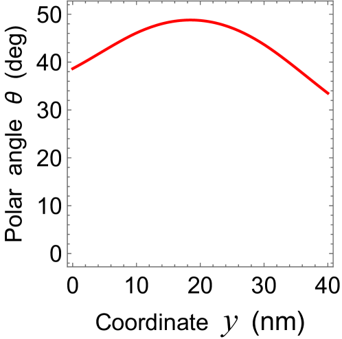
First, we employed the micromagnetic simulations for the determination of the initial magnetization orientation in the film. The study of the magnetization relaxation to an equilibrium direction showed that the magnetization is practically orthogonal to the surfaces in the absence of external magnetic fields. This is due to the influence of PMA, which is stronger than that of the demagnetizing field at the considered small thickness nm. Under the external field Oe, the magnetization rotates towards the film plane and becomes inhomogeneous across the waveguide (Fig. 2), having an elevation angle of at the center. The revealed significant inhomogeneity of the magnetic state is caused by the demagnetizing field , which is rather strong owing to the relatively small width nm of the waveguide. The calculations also show that the asymmetry of the magnetization distribution across the waveguide (Fig. 2) is due to the interfacial DMI.
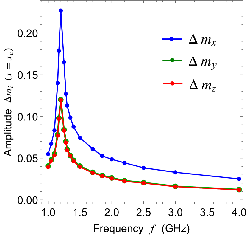
Next, we studied the electrically induced magnetic dynamics in the waveguide in the absence of a direct electric current in the layer. It was assumed that the top electrode with the dimensions nm2 deposited on the layer with the thickness nm is subjected to a microwave voltage . The voltage-induced modification of the PMA parameter associated with the interface beneath the electrode was taken into account for the corresponding computational cells. The calculations showed that the microwave voltage excites a steady-state magnetization precession () in the waveguide section under the top electrode. The quantities characterizing the precession amplitude averaged over the waveguide width maximize when the excitation frequency equals GHz (see Fig. 3). At frequencies the magnetization precession has an ellipticity , which is about 1.4 at the voltage amplitude V. It should be noted that the applied voltage creates a microwave tunnel current flowing through the barrier and the bilayer. Using the experimentally determined barrier conductance S m-2 [47], we find that this current has a density A m-2 in the 5-nm-thick layer at V. As confirmed by additional simulations, the SOT created by such an electric current does not significantly affect the magnetization dynamics in .
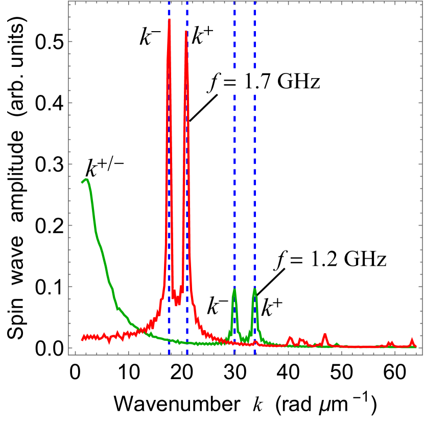
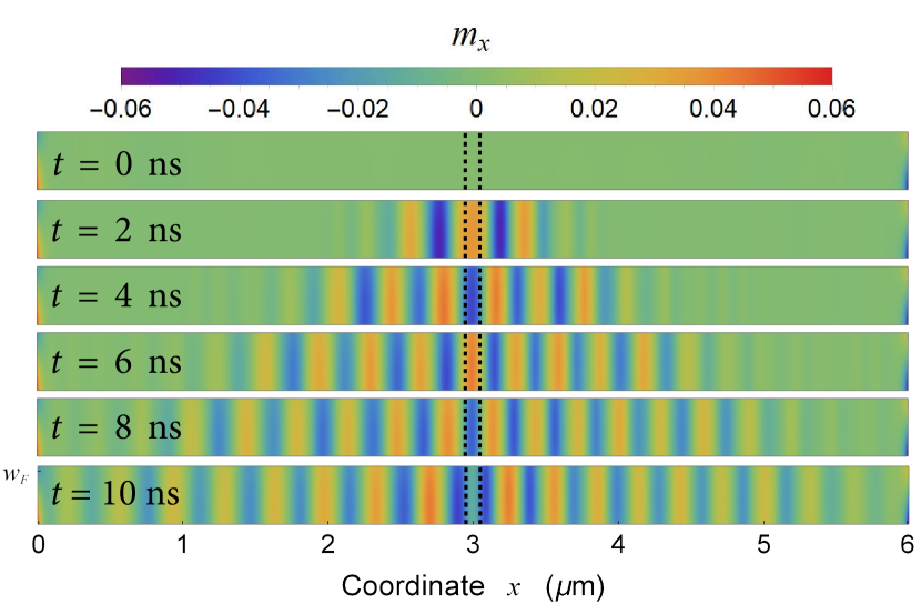
At the excitation frequencies below the resonance frequency , the electrically induced magnetization precession appears to be confined within the waveguide section under the top electrode. In contrast, the emission of spin waves from the excitation area was revealed at the frequencies . These waves travel in the opposite directions within two halves of the nanolayer. In the case of resonant excitation (), packets of spin-wave modes with various wave vectors propagate in the waveguide (see Fig. 4). However, well above the magnetization dynamics takes the form of a spin wave with a definite wavenumber or (Fig. 4). Therefore, further modeling was carried out at the excitation frequency GHz, at which the simulations yield rad m-1 and rad m-1. Figure 5 illustrates time evolutions of the two spin waves generated by the microwave voltage with such a frequency. Interestingly, despite significant difference between the wavenumbers and , the amplitudes of the two spin waves decrease very similarly with the distance from the waveguide center. The decay of the spin-wave amplitude, which is caused by the Gilbert damping, follows the exponential law with a high accuracy. The decay lengths and of spin waves with the wavenumbers and were found to be m. It should be noted that the revealed difference between and is due to the interfacial DMI. Such a difference was earlier predicted theoretically [48] and observed experimentally in the heterostructure [45].
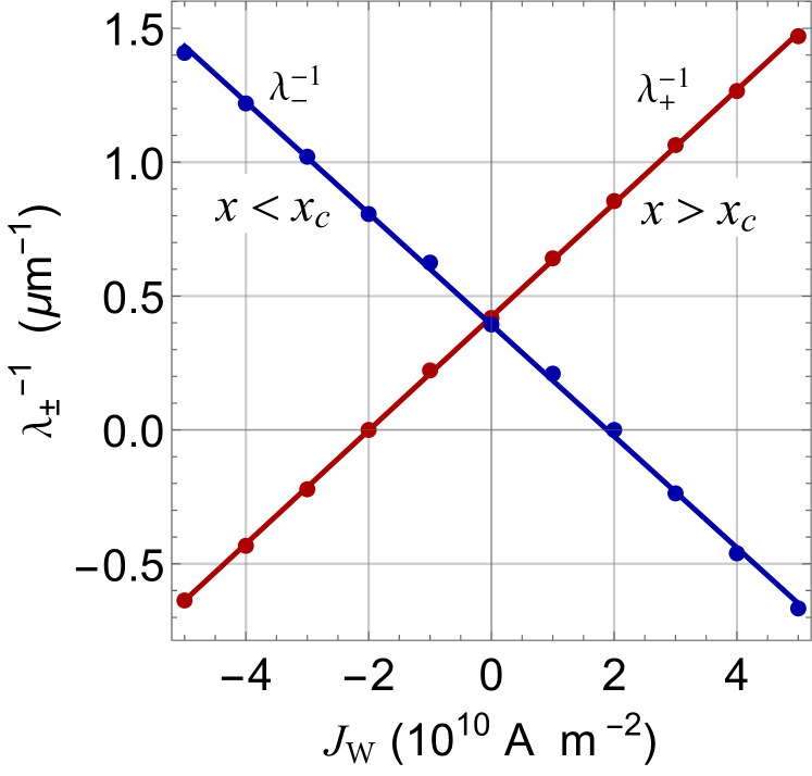
The most important results were obtained when studying the influence of the direct electric current flowing in the layer on the propagation of spin waves in the waveguide. For each predetermined density of this current, we modeled the excitation of spin waves by the microwave voltage locally modulating VCMA in the presence of SOT created by the spin current injected into the CoFeB nanolayer. In the simulations, the VCMA oscillating with the frequency GHz and time-independent SOT were simultaneously applied at the moment to the CoFeB nanolayer with the equilibrium magnetization distribution forming at and . The analysis of the electrically induced magnetization dynamics was limited by the time period ns, during which both spin waves reach the ends of the -m-long waveguide. It was found that SOT does not significantly change the wave numbers and of the generated spin waves. At small current densities , the amplitudes of these waves still decrease exponentially with the increasing distance from the waveguide center. However, their decay lengths and change under the action of SOT in the opposite way owing to different directions of the electric currents flowing in the underlying halves of the layer (Fig. 1), which affect the vector in Eq. (1). Namely, the spin wave decays faster when the quantity is positive and slower when it is negative. The simulation data show that the inverse decay lengths and vary linearly with the current density (see Fig. 6).
Remarkably, and go to zero at A m-2 and A m-2, respectively. Hence, the spin wave with the wave vector () travels with a constant amplitude at the critical current density () because the Gilbert damping is fully compensated by SOT. At overcritical current densities or , the amplitude of such a spin wave exponentially increases with the distance from the excitation area, which manifests itself in negative values of the decay lengths seen in Fig. 6.
Since SOT simultaneously reduces the positive decay length of another spin wave that travels in the opposite direction, by passing sufficient direct current through the layer it becomes possible to realize a long-distance spin-wave propagation in one half of the waveguide only. Moreover, by reversing the polarity of the dc voltage applied to the layer one can change the propagation region and switch the travel direction of the spin wave in the waveguide. To quantify the described effect, we determined the ratio of the precession amplitudes in the spin waves with the wavenumbers and at the same distance from the waveguide center. Variations of this ratio with the distance at different densities of the electric current are presented in Fig. 7.
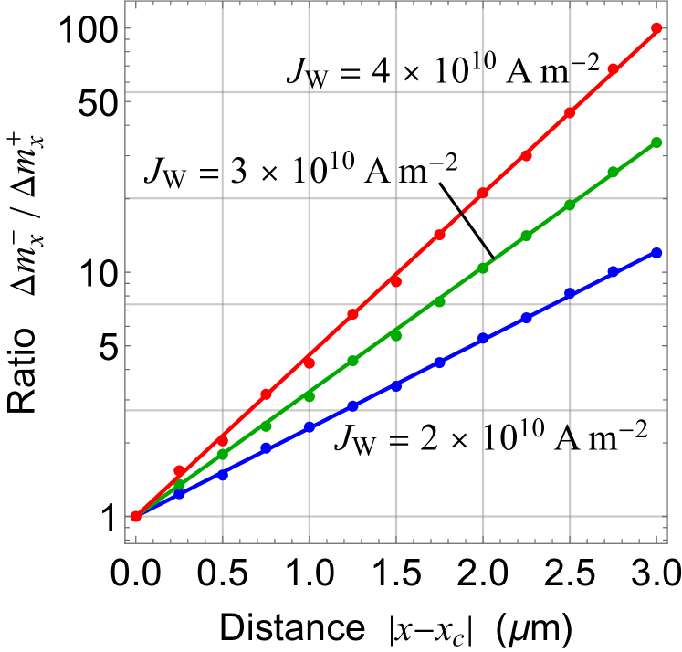
It is seen that the ratio exponentially increases with the distance from the source of spin waves, reaching 100 at m when A m-2. Since at GHz the propagation of monochromatic spin waves with definite wavenumbers takes place in the waveguide (see Fig. 4), the ratio of the amounts of power transmitted in the opposite directions at the distance simply equals the square of the corresponding number given in Fig. 7.
To clarify the optimal conditions for the SOT-induced amplification of spin waves in the waveguide, we studied the dependence of the critical current densities and on the strength of the external in-plane magnetic field.
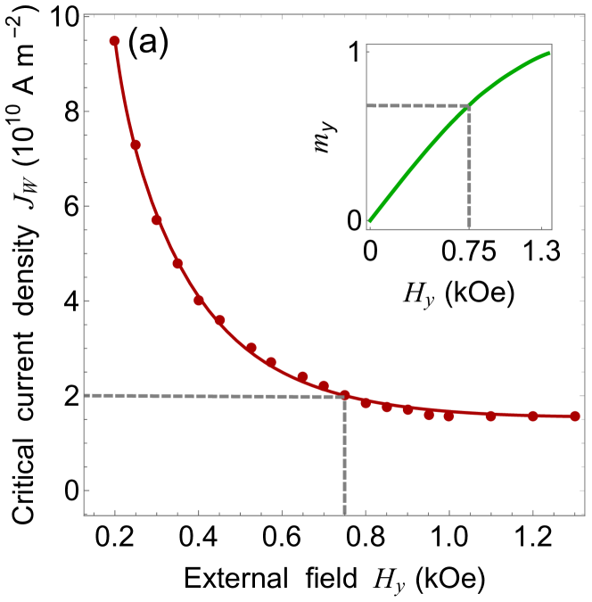
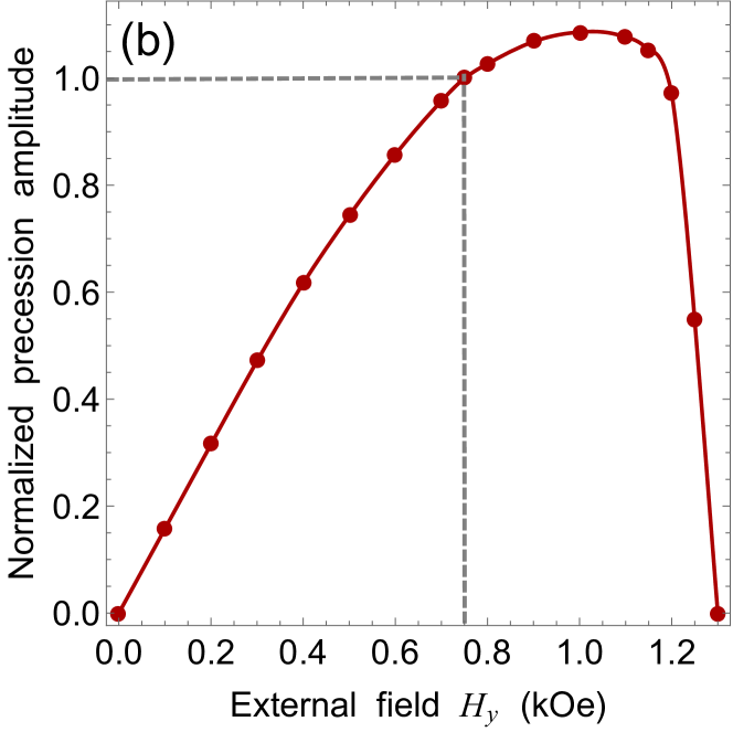
The simulations showed that the magnitude of critical densities monotonically decreases with increasing field strength [see Fig. 8 (a)]. However, this decrease is accompanied by a gradual rotation of the equilibrium magnetization direction in the layer towards the in-plane orientation [see inset in Fig. 8 (a)]. Owing to such a rotation, the amplitude of magnetization precession in the waveguide varies nonmonotonically with increasing . As demonstrated by Fig. 8 (b), the precession amplitude becomes maximal at kOe and decreases drastically when the field strength exceeds 1.2 kOe. Therefore, the applied magnetic field should not be higher than 1.2 kOe so that the lowest acceptable magnitude of the critical current densities amounts to about A m-2. This result shows that the chosen field strength Oe provides almost minimal critical current density in the W layer in addition to almost maximal precession amplitude in the waveguide.
Discussing our theoretical results in the light of available experimental data, we note that a strong effect of SOT on the propagation of spin waves was observed in the Yttrium Iron Garnet (YIG) waveguide [14]. It was found that the spin-wave decay length could be increased by nearly a factor of 10 by passing an electric current through the layer adjacent to the YIG film. Up to some threshold current, the inverse decay length decreases linearly with the current magnitude, but then begins to increase instead of tending to zero [14]. The absence of the expected compensation of the magnetic damping by SOT was attributed to the enhancement of magnetic fluctuations by SOT, which becomes important at large currents [17]. In the YIG system, however, the estimated current density providing the damping compensation is about 16 times larger than the critical density A m-2 that we predict for the current flowing in the layer of the heterostructure. Furthermore, the maximal amplitude of the magnetization precession in our simulations does not exceed 0.15, and the precession ellipticity is about 1.4 only. These values explain the SOT-induced amplification of spin waves, which was revealed in our simulations during a short time period ns in the absence of thermal fluctuations. Indeed, recent study of the magnetization dynamics in ferromagnetic disks demonstrated that the nonlinear damping could be suppressed by minimizing the precession ellipticity even at amplitudes exceeding 0.15 [49].
However, a longer modeling demonstrates the progressive development of magnetization auto-oscillations in the CoFeB layer at the current densities and . The amplitude of these oscillations strongly increases at the time ns after the application of SOT, which leads to the transfer of the spin-wave power to incoherent auto-oscillations with higher frequencies due to the magnon-magnon scattering. As a result, the spin-wave amplitude now decreases with the distance from the excitation area even at the highest current density A m-2 used in our simulations. Thus, the compensation of the pronounced nonlinear damping by SOT appears to be impossible [17], but the SOT-induced amplification of spin waves during several nanoseconds should be feasible in the W/CoFeB/MgO nanostructure. This prediction is corroborated by the recent experimental demonstration of the spin-wave amplification by short SOT pulses in the YIG/Pt waveguide [50].
To check whether the temporary amplification of spin waves in the W/CoFeB/MgO nanostructure is also possible in the presence of thermal fluctuations, we carried out additional simulations, in which the effective field involved in Eq. (1) was appended by the contribution of a thermal random field [51]. The simulations were performed using MuMax3 software [52] for the 30-m-long waveguide kept at the temperature K. To increase the stability of the out-of-plane magnetization state against deflections caused by thermal fluctuations, the CoFeB width was increased from 40 to 100 nm.
An applied magnetic field with the components Oe and Oe was introduced to ensure efficient nonparametric generation of spin waves by the modulation of VCMA at the frequencies above the resonance frequency, which amounts to 5.1 GHz at such a field. In addition, the periodic boundary conditions were employed to get rid of spin-wave reflections at the waveguide ends.
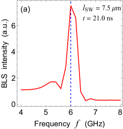
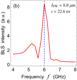
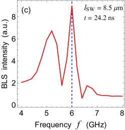
The simulations executed for a representative excitation frequency GHz and various densities A m-2 of the electric current in the W layer demonstrated the generation of both monochromatic spin waves and incoherent magnetization oscillations in the CoFeB layer. Since the CoFeB thickness is very small, the influence of thermal fluctuations on the magnetic dynamics appears to be strong at K. Therefore, the quantification of the spin-wave amplitude requires some averaging procedure. Since the propagation of spin waves in ferromagnets can be visualized with the aid of the micro-focus Brillouin light scattering (BLS) spectroscopy [53], we calculated the BLS intensity corresponding to the magnetization dynamics predicted by our simulations. Using the computational technique described in Ref. [54], we obtained frequency spectra of the BLS intensities at the fronts of two propagating spin waves at different times after their generation in the waveguide center. The representative spectra presented in Fig. 9 demonstrate the existence of two pronounced peaks, one of which is centered around the excitation frequency GHz, whereas the other is located at a frequency GHz close to the resonance frequency GHz of the CoFeB layer. Since the background BLS intensity independent of frequency and spatial location was subtracted from the spectra shown in Fig. 9, the height of the first peak quantifies the intensity of the spin wave at the position of its front. In contrast, the second peak characterizes the magnetization auto-oscillations developed during the time period of the spin-wave-propagation in the waveguide. The comparison of the three spectra presented in Fig. 9 shows that the intensity of such oscillations rapidly grows with time and approaches the spin-wave intensity after about 24 ns.
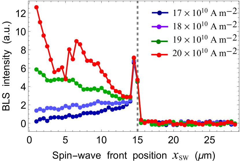
Representative dependences of the BLS intensity at the frequency GHz on the position of the spin-wave front in the waveguide are shown in Fig. 10. Remarkably, they demonstrate that, when the current density in the heavy-metal layer is high enough ( A m-2), the intensity of the spin wave propagating in the left half of the waveguide significantly increases with the distance from the excitation area. Thus, the temporal amplification of spin waves by SOT should be feasible in the W/CoFeB/MgO nanostructure even at room temperature.
IV Conclusion
In this work, we theoretically studied the electrical excitation and control of spin waves in a ferromagnetic waveguide. The study was carried out for the nanostructure having PMA and DMI associated with the and interfaces, respectively. Using micromagnetic simulations based on the numerical solution of the modified Landau-Lifshitz-Gilbert equation, we showed that the modulation of PMA by a microwave voltage locally applied to the layer renders it possible to generate two spin waves propagating in the opposite directions from the center of the waveguide. Although owing to DMI these waves have different wavenumbers (21.08 rad m-1 vs. 17.42 rad m-1 at GHz), they retain similar decay lengths of about 2.5 m. It should be noted that, in contrast to the previous theoretical works [10, 55], the VCMA-driven excitation of spin waves is not parametric in our simulations. Due to the inclined magnetization direction in the ferromagnetic layer (Fig. 1), the spin-wave generation takes place even at small amplitudes of the microwave voltage unlike the parametric excitation, which requires the voltage amplitude exceeding some threshold value [10, 55]. Furthermore, the simulations demonstrated that the propagation lengths of spin waves in the layer can be changed drastically by passing a direct electric current through the adjacent film. Depending on the direction of the electric current and that of the effective field , the propagation length either increases or decreases due to the SOT acting on the magnetization. Importantly, complete compensation of the magnetic damping by the SOT-induced antidamping temporarily occurs at the critical current density, which amounts to about A m-2 at K and A m-2 at K. This remarkable feature of the heterostructure opens the possibility of efficient electrical control of the spin-wave propagation in the layer. Hence, this nanostructure represents a promising waveguide, in which the amplification and long-range propagation of spin waves could be achieved in practice.
If the electric current is locally injected into the heavy-metal layer near the waveguide center, the charge flow has opposite directions in the two halves of this layer (Fig. 1). Therefore, the spin waves travelling in the adjacent halves of the waveguide experience the action of SOTs having opposite directions. Because of such SOT inhomogeneity, it becomes possible to strongly increase the propagation length of one of these waves, while simultaneously creating a fast decay of the other wave. The simulations show that at K the ratio of the amplitudes of magnetization precession at the two ends of the 6-m-long waveguide reaches 100 at the current density A m-2. Hence, significant spin-wave signal can be sent to one of the waveguide ends only. Moreover, the signal transmission can be switched to the other end by changing the polarity of the dc voltage applied to the heavy-metal layer. Thus, the studied nanostructure represents an electrically controlled magnonic device that converts the electrical input signal into a spin signal, which can be transmitted to one of two outputs. Since such a device does not employ oscillating magnetic fields, it may have relatively low power consumption, which should facilitate its applications in magnonics.
V ACKNOWLEDGMENT
We thank Dr. Vladislav E. Demidov for valuable comments on our micromagnetic simulations of the spin-wave amplification in the presence of spin-orbit torque.
References
- Neusser and Grundler [2009] S. Neusser and D. Grundler, Magnonics: Spin Waves on the Nanoscale, Advanced Materials 21, 2927 (2009).
- Chumak et al. [2015] A. Chumak, V. Vasyuchka, A. Serga, and B. Hillebrands, Magnon spintronics, Nat. Phys. 11, 453 (2015).
- Csaba et al. [2017] G. Csaba, Ádám Papp, and W. Porod, Perspectives of using spin waves for computing and signal processing, Phys. Lett. A 381, 1471 (2017).
- Demidov et al. [2011] V. E. Demidov, M. P. Kostylev, K. Rott, J. Münchenberger, G. Reiss, and S. O. Demokritov, Excitation of short-wavelength spin waves in magnonic waveguides, Appl. Phys. Lett. 99, 082507 (2011).
- Yu et al. [2016] H. Yu, O. d’ Allivy Kelly, V. Cros, R. Bernard, P. Bortolotti, A. Anane, F. Brandl, F. Heimbach, and D. Grundler, Approaching soft X-ray wavelengths in nanomagnet-based microwave technology, Nat. Commun. 7, 11255 (2016).
- Liu et al. [2018] C. Liu, J. Chen, T. Liu, F. Heimbach, H. Yu, Y. Xiao, J. Hu, M. Liu, H. Chang, T. Stueckler, S. Tu, Y. Zhang, Y. Zhang, P. Gao, Z. Liao, D. Yu, K. Xia, N. Lei, W. Zhao, and M. Wu, Long-distance propagation of short-wavelength spin waves, Nat. Commun. 9, 738 (2018).
- Demidov et al. [2010] V. Demidov, S. Urazhdin, and S. Demokritov, Direct observation and mapping of spin waves emitted by spin-torque nano-oscillators, Nature Mater. 9, 984 (2010).
- Madami et al. [2011] M. Madami, S. Bonetti, G. Consolo, S. Tacchi, G. Carlotti, G. Gubbiotti, F. B. Mancoff, M. A. Yar, and J. Åkerman, Direct observation of a propagating spin wave induced by spin-transfer torque, Nature Nanotech. 6, 635 (2011).
- Zhou et al. [2019] Z.-w. Zhou, X.-g. Wang, Y.-z. Nie, Q.-l. Xia, Z.-m. Zeng, and G.-h. Guo, Left-handed polarized spin waves in ferromagnets induced by spin-transfer torque, Phys. Rev. B 99, 014420 (2019).
- Verba et al. [2014] R. Verba, V. Tiberkevich, I. Krivorotov, and A. Slavin, Parametric Excitation of Spin Waves by Voltage-Controlled Magnetic Anisotropy, Phys. Rev. Applied 1, 044006 (2014).
- Divinskiy et al. [2018] B. Divinskiy, V. E. Demidov, S. Urazhdin, R. Freeman, A. B. Rinkevich, and S. O. Demokritov, Excitation and Amplification of Spin Waves by Spin–Orbit Torque, Advanced Materials 30, 1802837 (2018).
- Fulara et al. [2019] H. Fulara, M. Zahedinejad, R. Khymyn, A. Awad, S. Muralidhar, M. Dvornik, and J. Åkerman, Spin-orbit torque–driven propagating spin waves, Sci. Advances 5, 9 (2019).
- An et al. [2014] K. An, D. R. Birt, C.-F. Pai, K. Olsson, D. C. Ralph, R. A. Buhrman, and X. Li, Control of propagating spin waves via spin transfer torque in a metallic bilayer waveguide, Phys. Rev. B 89, 140405 (2014).
- Evelt et al. [2016] M. Evelt, V. E. Demidov, V. Bessonov, S. O. Demokritov, J. L. Prieto, M. Muñoz, J. B. Youssef, V. V. Naletov, G. de Loubens, O. Klein, M. Collet, K. Garcia-Hernandez, P. Bortolotti, V. Cros, and A. Anane, High-efficiency control of spin-wave propagation in ultra-thin yttrium iron garnet by the spin-orbit torque, Appl. Phys. Lett. 108, 172406 (2016).
- Wimmer et al. [2019] T. Wimmer, M. Althammer, L. Liensberger, N. Vlietstra, S. Geprägs, M. Weiler, R. Gross, and H. Huebl, Spin Transport in a Magnetic Insulator with Zero Effective Damping, Phys. Rev. Lett. 123, 257201 (2019).
- Navabi et al. [2019] A. Navabi, Y. Liu, P. Upadhyaya, K. Murata, F. Ebrahimi, G. Yu, B. Ma, Y. Rao, M. Yazdani, M. Montazeri, L. Pan, I. N. Krivorotov, I. Barsukov, Q. Yang, P. Khalili Amiri, Y. Tserkovnyak, and K. L. Wang, Control of Spin-Wave Damping in YIG Using Spin Currents from Topological Insulators, Phys. Rev. Applied 11, 034046 (2019).
- Demidov et al. [2020] V. E. Demidov, S. Urazhdin, A. Anane, V. Cros, and S. O. Demokritov, Spin–orbit-torque magnonics, Journal of Appl. Phys. 127, 170901 (2020).
- Manchon et al. [2019] A. Manchon, J. Železný, I. M. Miron, T. Jungwirth, J. Sinova, A. Thiaville, K. Garello, and P. Gambardella, Current-induced spin-orbit torques in ferromagnetic and antiferromagnetic systems, Rev. Mod. Phys. 91, 035004 (2019).
- Mahmoud et al. [2020] A. Mahmoud, F. Ciubotaru, F. Vanderveken, A. V. Chumak, S. Hamdioui, C. Adelmann, and S. Cotofana, Introduction to spin wave computing, Journal of Appl. Phys. 128, 161101 (2020).
- Chumak et al. [2014] A. V. Chumak, A. A. Serga, and B. Hillebrands, Magnon transistor for all-magnon data processing, Nat. Commun. 5 (2014).
- Balinskiy et al. [2018] M. Balinskiy, H. Chiang, and A. Khitun, Realization of spin wave switch for data processing, AIP Advances 8, 056628 (2018).
- Vogt et al. [2014] K. Vogt, F. Fradin, J. Pearson, T. Sebastian, S. Bader, B. Hillebrands, A. Hoffmann, and H. Schultheiss, Realization of a spin-wave multiplexer, Nat. Commun. 5, 3727 (2014).
- Sadovnikov et al. [2015] A. V. Sadovnikov, C. S. Davies, S. V. Grishin, V. V. Kruglyak, D. V. Romanenko, Y. P. Sharaevskii, and S. A. Nikitov, Magnonic beam splitter: The building block of parallel magnonic circuitry, Appl. Phys. Lett. 106, 192406 (2015).
- Davies et al. [2015] C. S. Davies, A. V. Sadovnikov, S. V. Grishin, Y. P. Sharaevsky, S. A. Nikitov, and V. V. Kruglyak, Field-controlled phase-rectified magnonic multiplexer, IEEE Trans. Magn. 51, 1 (2015).
- Wang et al. [2018] Q. Wang, P. Pirro, R. Verba, A. Slavin, B. Hillebrands, and A. V. Chumak, Reconfigurable nanoscale spin-wave directional coupler , Sci. Adv. 4, e1701517 (2018).
- Hamadeh et al. [2014] A. Hamadeh, O. d’Allivy Kelly, C. Hahn, H. Meley, R. Bernard, A. H. Molpeceres, V. V. Naletov, M. Viret, A. Anane, V. Cros, S. O. Demokritov, J. L. Prieto, M. Muñoz, G. de Loubens, and O. Klein, Full Control of the Spin-Wave Damping in a Magnetic Insulator Using Spin-Orbit Torque, Phys. Rev. Lett. 113, 197203 (2014).
- Sklenar et al. [2016] J. Sklenar, W. Zhang, M. B. Jungfleisch, W. Jiang, H. Saglam, J. E. Pearson, J. B. Ketterson, and A. Hoffmann, Perspective: Interface generation of spin-orbit torques, Journal of Appl. Phys. 120, 180901 (2016).
- Tserkovnyak et al. [2002] Y. Tserkovnyak, A. Brataas, and G. E. W. Bauer, Enhanced gilbert damping in thin ferromagnetic films, Phys. Rev. Lett. 88, 117601 (2002).
- Kittel [1949] C. Kittel, Physical theory of ferromagnetic domains, Rev. Mod. Phys. 21, 541 (1949).
- Azovtsev and Pertsev [2016] A. V. Azovtsev and N. A. Pertsev, Magnetization dynamics and spin pumping induced by standing elastic waves, Phys. Rev. B 94, 184401 (2016).
- Ikeda et al. [2010] S. Ikeda, K. Miura, H. Yamamoto, K. Mizunuma, H. D. Gan, M. Endo, S. Kanai, J. Hayakawa, F. Matsukura, and H. Ohno, A perpendicular-anisotropy magnetic tunnel junction, Nat. Mater 9, 721 (2010).
- Alzate et al. [2014] J. G. Alzate, P. Khalili Amiri, G. Yu, P. Upadhyaya, J. A. Katine, J. Langer, B. Ocker, I. N. Krivorotov, and K. L. Wang, Temperature dependence of the voltage-controlled perpendicular anisotropy in nanoscale magnetic tunnel junctions, Appl. Phys. Lett. 104, 112410 (2014).
- Pertsev [2013] N. A. Pertsev, Origin of easy magnetization switching in magnetic tunnel junctions with voltage-controlled interfacial anisotropy, Sci. Rep. 3, 2757 (2013).
- Cortés-Ortuño et al. [2018] D. Cortés-Ortuño, M. Beg, V. Nehruji, L. Breth, R. Pepper, T. Kluyver, G. Downing, T. Hesjedal, P. Hatton, T. Lancaster, R. Hertel, O. Hovorka, and H. Fangohr, Proposal for a micromagnetic standard problem for materials with dzyaloshinskii–moriya interaction, New Journal of Physics 20, 113015 (2018).
- Perez et al. [2014] N. Perez, L. Torres, and E. Martinez-Vecino, Micromagnetic modeling of dzyaloshinskii–moriya interaction in spin hall effect switching, IEEE Transactions on Magnetics 50, 1 (2014).
- Rohart and Thiaville [2013] S. Rohart and A. Thiaville, Skyrmion confinement in ultrathin film nanostructures in the presence of dzyaloshinskii-moriya interaction, Phys. Rev. B 88, 184422 (2013).
- Vandermeulen et al. [2016] J. Vandermeulen, S. A. Nasseri, B. V. de Wiele, G. Durin, B. V. Waeyenberge, and L. Dupré, The effect of dzyaloshinskii–moriya interaction on field-driven domain wall dynamics analysed by a semi-analytical approach, Journal of Physics D: Applied Physics 49, 465003 (2016).
- Haney et al. [2013] P. M. Haney, H.-W. Lee, K.-J. Lee, A. Manchon, and M. D. Stiles, Current induced torques and interfacial spin-orbit coupling: Semiclassical modeling, Phys. Rev. B 87, 174411 (2013).
- Kim et al. [2020] C. Kim, B. S. Chun, J. Yoon, D. Kim, Y. J. Kim, I. H. Cha, G. W. Kim, D. H. Kim, K.-W. Moon, Y. K. Kim, and C. Hwang, Spin-orbit torque driven magnetization switching and precession by manipulating thickness of heterostructures, Advanced Electronic Materials 6, 1901004 (2020).
- Giancoli [1995] D. Giancoli, Physics: Principles with Applications, Prentice-Hall International editions (Prentice Hall, 1995).
- Fan et al. [2014] X. Fan, H. Celik, J. Wu, C. Ni, K.-J. Lee, V. O. Lorenz, and J. Q. Xiao, Quantifying interface and bulk contributions to spin–orbit torque in magnetic bilayers, Nat. Commun. 5, 3042 (2014).
- Lee et al. [2011] K. Lee, J. J. Sapan, S. H. Kang, and E. E. Fullerton, Perpendicular magnetization of on single-crystal , Journal of Appl. Phys. 109, 123910 (2011).
- Sato et al. [2012] H. Sato, M. Yamanouchi, K. Miura, S. Ikeda, R. Koizumi, F. Matsukura, and H. Ohno, Cofeb thickness dependence of thermal stability factor in perpendicular magnetic tunnel junctions, IEEE Magnetics Letters 3, 3000204 (2012).
- Hall [1960] R. C. Hall, Magnetic anisotropy and magnetostriction of ordered and disordered cobalt-iron alloys, Journal of Appl. Phys. 31, S157 (1960).
- Chaurasiya et al. [2016] A. K. Chaurasiya, C. Banerjee, S. Pan, S. Sahoo, S. Choudhury, J. Sinha, and A. Barman, Direct observation of interfacial dzyaloshinskii-moriya interaction from asymmetric spin-wave propagation in heterostructures down to sub-nanometer cofeb thickness, Sci. Rep. 6, 32592 (2016).
- Jhajhria et al. [2019] D. Jhajhria, N. Behera, D. K. Pandya, and S. Chaudhary, Dependence of spin pumping in heterostructures on the structural phase of tungsten, Phys. Rev. B 99, 014430 (2019).
- Yang et al. [2010] J. Yang, R. J. Macedo, M. G. Debs, R. Ferreira, S. Cardoso, P. J. P. Freitas, J. M. Teixeira, and J. O. Ventura, Spin transfer on low resistance-area -based magnetic tunnel junctions prepared by ion beam deposition, IEEE Transactions on Magnetics 46, 2002 (2010).
- Moon et al. [2013] J.-H. Moon, S.-M. Seo, K.-J. Lee, K.-W. Kim, J. Ryu, H.-W. Lee, R. D. McMichael, and M. D. Stiles, Spin-wave propagation in the presence of interfacial dzyaloshinskii-moriya interaction, Phys. Rev. B 88, 184404 (2013).
- Divinskiy et al. [2019] B. Divinskiy, S. Urazhdin, S. O. Demokritov, and V. E. Demidov, Controlled nonlinear magnetic damping in spin-Hall nano-devices, Nat. Commun. 10 (2019).
- Merbouche et al. [2023] H. Merbouche, B. Divinskiy, D. Gouéré, R. Lebrun, A. El-Kanj, V. Cros, P. Bortolotti, A. Anane, S. O. Demokritov, and V. E. Demidov, True amplification of spin waves in magnonic nano-waveguides (2023), arXiv:2303.04695 [cond-mat.mes-hall] .
- Ito et al. [2006] K. Ito, T. Devolder, C. Chappert, M. J. Carey, and J. A. Katine, Probabilistic behavior in subnanosecond spin transfer torque switching, Journal of Applied Physics 99, 08G519 (2006).
- Vansteenkiste et al. [2014] A. Vansteenkiste, J. Leliaert, M. Dvornik, M. Helsen, F. Garcia-Sanchez, and B. Van Waeyenberge, The design and verification of MuMax3, AIP Advances 4, 107133 (2014).
- Demidov and Demokritov [2015] V. E. Demidov and S. O. Demokritov, Magnonic waveguides studied by microfocus brillouin light scattering, IEEE Transactions on Magnetics 51, 1 (2015).
- Wojewoda et al. [2023] O. Wojewoda, F. Ligmajer, M. Hrtoň, J. Klíma, M. Dhankhar, K. Davídková, M. Staňo, J. Holobrádek, J. Krčma, J. Zlámal, T. Šikola, and M. Urbánek, Observing high-k magnons with mie-resonance-enhanced brillouin light scattering, Commun Phys 6, 94 (2023).
- Verba et al. [2017] R. Verba, M. Carpentieri, G. Finocchio, V. Tiberkevich, and A. Slavin, Excitation of Spin Waves in an In-Plane-Magnetized Ferromagnetic Nanowire Using Voltage-Controlled Magnetic Anisotropy, Phys. Rev. Applied 7, 064023 (2017).