Frequency to power conversion by an electron turnstile
Direct frequency to power conversion (FPC), to be presented here, links both quantities through a known energy, like single-electron transport relates an operation frequency to the emitted current through the electron charge as Geerligs1990; Kouwenhoven1991; Pekola2007; Pekola2013; Kaestner2015; Giblin2020. FPC is a natural candidate for a power standard resorting to the most basic definition of the watt– energy, which is traceable to Planck’s constant , emitted per unit of time. This time is in turn traceable to the unperturbed ground state hyperfine transition frequency of the caesium 133 atom ; hence, FPC comprises a simple and elegant way to realize the watt SI. In this spirit, single-photon emission and detection at known rates have been proposed and experimented as radiometric standard Zwinkels2010; Chunnilall2014; Vaigu2017; Rodiek2017; Lemieux2019; Saha2020; Zhu2020; Tomm2021. However, nowadays power standards are only traceable to electrical units, i.e., volt and ohm Palafox2007; Waltrip2009; SI; Waltrip2021. In this letter, we demonstrate the feasibility of an alternative proposal based on solid-state direct FPC using a SINIS (S = superconductor, N = normal metal, I = insulator) single-electron transistor (SET) accurately injecting (integer) quasiparticles (qps) per cycle to both leads with discrete energies close to their superconducting gap , even at zero drain-source voltage. Furthermore, the bias voltage plays an important role in the distribution of the power among the two leads, allowing for an almost equal injection to the two. We estimate that under appropriate conditions errors can be well below .
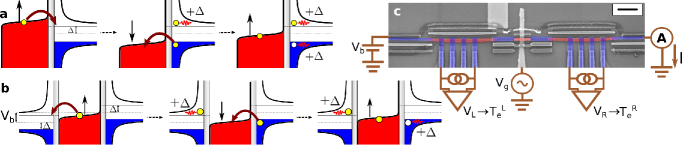
The FPC relation can be understood based on a simplified picture of a driven NIS junction (Fig. 1a) by looking at the qp injection dynamics. The key property here is the singularity of the superconducting density of states at energies as counted from the Fermi level. During the driving period where the chemical potential of N is periodically shifted, an electron tunnels into the superconductor with energy due to this diverging density of states. Later on, the driving provides enough energy for an electron to tunnel into the island breaking a Cooper pair and leaving an excitation in the superconductor, again close to the gap-edge. Thus, two tunnelling events per cycle occur; for larger driving amplitudes a higher even number of tunnelling events is allowed. Within this picture, if a second superconducting lead is tunnel coupled to the island, the tunnelling events at bias voltage occur stochastically through either junction with probabilities proportional to each junction transparency. This whole operation results in total energy injection of nearly in each cycle in the absence of net current. The case for a biased () SINIS SET is depicted in Figure 1b in which the qp injection events happen analogously to panel a. The only difference is that the bias defines a preferred direction for the charge transfer and therefore there will be tunnelling events per junction, i.e., the junction transparency does not play a key role anymore. The total energy injected is distributed almost equally to both leads but remains (nearly) unchanged. Time-averaged, the total injected energy current would be given by
| (1) |
and would exhibit a structure of plateaus similar to the charge current pumped through SINIS turnstiles Pekola2007, but now even at zero bias voltage. Accuracy of Eq. (1) can be tested in the FPC device depicted in Fig. 1c (see Supplementary Section S1 for its characterization).
This device constitutes a turnstile for single electrons (see Supplementary Figure S1) when the island (light red short structure in Figure 1c) is periodically driven at frequency with a radio-frequency (rf) signal applied to a capacitively coupled, via the capacitance , gate electrode. At proper source-drain biases and driving amplitudes, an average charge current is obtained. This current is transported by qps injected per second to both tunnel-contacted leads (light blue short structure in Fig. 1c), respectively. The qps transport energy approximately without losses across the narrow leads Peltonen2010; Knowles2012 to directly interfaced normal-metal traps (light red long structures). These structures act as bolometers for measuring quantitatively the heat generated by the qp injection, accounting completely for the power Ullom2000. This heat can be determined within the conventional normal-metal electron-phonon interaction model Giazotto2006 as . Here is the electron-phonon coupling constant of the material, the trap volume, its electron temperature and the phonon bath temperature which usually can be taken as the cryostat temperature Dorozhkin1986. The bolometer factor is calibrated in-situ with an uncertainty . See Supplementary Section S2 for details on the calibration of this detector. is in turn obtained by current-biasing the superconducting tunnel probes (vertical blue structures in Fig. 1c) contacted to the trap and measuring the corresponding voltage drop (see Supplementary Section S3 for the temperature calibration of these thermometers). The measured power can be compared to the expected FPC outcome.
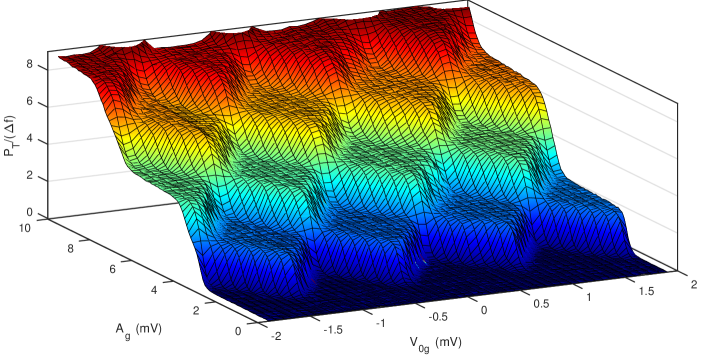
The main result of this work is shown in Fig. 2 where the total injected power (to the left plus to the right lead ) measured with the bolometers is shown. This was measured with a gate signal at and , hence no net charge (particle) current flows through the SET. Here, the DC gate voltage is swept over various gate periods revealing the -periodic nature of the injected energy. Simultaneously, the signal amplitude is varied so that the gate-induced charge spans several charge stability regions in the Coulomb diamonds of the SET. The measured injected power exhibits plateaus of (approximately) constant value against and , following closely Eq. (1) confirming the dynamics described in Figs. 1a and 1b. Therefore, we can assert that excitations are being injected close to the superconductor gap edge. The similarity of the plateaux pattern with that of Figure 2a in Ref. Pekola2007 is evident and shows parallelism between the frequency to current conversion of single-electron transport and our proposal of frequency to power conversion, the latter being possible at wider bias ranges including .
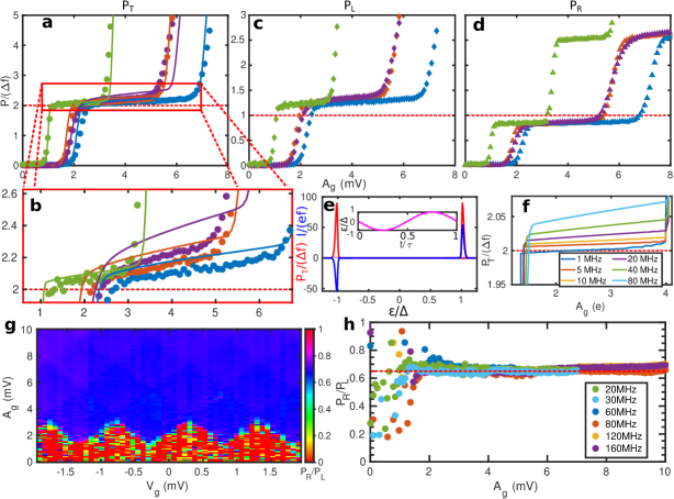
Further measurements of the power production at zero bias are shown in Fig. 3. Panel 3a shows the total injected power with at gate open position for a wide range of driving frequencies and confirms the results of Fig. 2 at different injected powers. The transmission of the rf gate voltage depends on frequency giving different dependences of the otherwise similar power (and current) curves for different frequencies. Panel b shows that the total generated energy is close to ideal FPC. Indeed, the conversion errors range from to at low frequency and from to at higher frequency . Calculations (solid lines) of the generated power resulting from a Markovian model (used also for DC characterization, See Supplementary Section S4) can reproduce the gate amplitude and frequency dependencies. Panels c and d exhibit the individual contributions to the power in the left and right lead, respectively. Notice that the two are not equal as explained above.
More insight into the dynamics of the zero bias operation is gained by simulating the instantaneous behaviour of the device. Figure 3e shows the calculated time dependent total injected power (Eq. (5), red curve) and current through one junction (Eq. (4), blue curve) plotted against the instantaneous energy change of an electron tunnelling into the island . Here is the system charging energy and is the normalized island excess charge induced by the gate voltage. A driving signal with offset equivalent to , as used for most of the measurements at , and period induces the evolution in shown in the inset of Figure 3e for a driving amplitude at the start of the first plateau. It is clear that only electrons within a narrow energy band around tunnel in and out of the island through the same junction, cancelling current and injecting an energy per event as postulated. Naturally, the tunnelling events can happen through any junction. How often a given junction is involved depends on the relative transparencies to be explained below.
Although the measured total injected powers shown in Figs. 2 and 3a are not exactly in the first plateau, we show in Fig. 3f that a system with proper , total normal-state junction resistance and Dynes parameter Dynes1978 can inject a power closer to this value. In this panel the total injected power for a device with , and was calculated solving the same Markovian model used so far with low but achievable temperatures (, for left and right lead and island, respectively). From there it is possible to see that when the driving is slow enough () the accuracy of the injected power is within and in the first plateau and between and for . Therefore it is possible, in principle, to achieve a power injection of with small deviations given that is sufficiently small and temperatures are low. Under these conditions the ultimate limitation of accuracy would then be determined by the capability of measuring small powers bolometrically: at the power is which exceeds the noise level in a standard setup by two orders of magnitude Ronzani2018. The bolometer noise is dominant over the shot noise of the generated energy flux caused by the stochastic nature of electron tunnelling, see Supplementary Section S5. Yet at these operation frequencies the Dynes parameter starts to play an important role making the power to be lower than Eq. (1). Additionally, we have verified that injection errors scale as , thus higher power emission with smaller inaccuracy is possible for more transparent junctions. Yet in this argument we ignore the influence of Andreev tunnelling power injection Rajauria2008.
How the power is distributed to the two leads can be easily understood within the Markovian model (see details in Supplementary Section S6). The absence of a preferred direction of flow (i.e., the bias voltage) together with assuming the same qp temperature for both leads yield
| (2) |
Where is the normal-state left (right) junction resistance. For the present device, we determined by the DC characterization . The ratios shown in Figs. 3g (calculated from data of Fig. 2) and 3h (from data in Figs. 3c and 3d) match this value, validating Eq. (2). Thus, the power is distributed according to the ratio of junction transparencies. Notice the insensitivity of this quantity to gate parameters or temperature.
Next, we turn to the case . Figure 4 shows two paradigmatic cases in panels a and b (see Supplementary Section S7 for additional data). In the former, the driving is slow enough to enable fully synchronized tunnelling in the direction of bias, avoiding back-tunnelling (i.e., tunnelling against the bias). In the latter, the driving frequency is fast such that forward tunnelling is compromised and back-tunnelling may take place instead. As a result, the pumped current drops toward the end of the plateau.
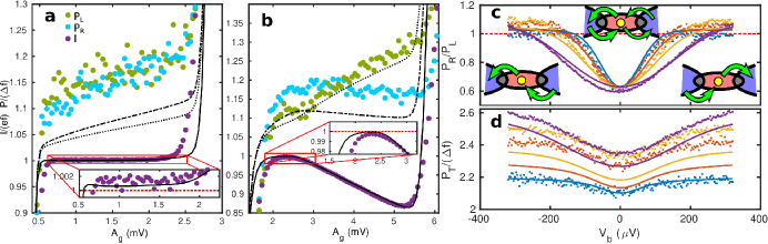
In Fig. 4a driving at and was applied, avoiding the back-tunnelling. An accurate single-electron current (purple dots) is emitted whose behaviour is well described by our simulations (solid black line, see inset). Similarly to the zero bias case, Eq. (1) is closely followed (see green and cyan dots for left and right leads, respectively), however now the main difference lies in how the injected energy is distributed between the leads. The bias, and consequently a preferred direction of tunnelling enable an almost equal share in the power injection to both leads, following the dynamics described in Fig. 1b. Both experiment and simulations show that now the distribution of the power has been inverted with respect to the zero bias case, i.e. . This can be explained by arguing that more energy needs to be provided for tunnelling through the more resistive junction, which is bound to happen under the present conditions before a back-tunnelling event can occur through the more transparent junction. In terms of Fig. 3e the power peaks move to .
On the other hand, data in Fig. 4b were measured with and . Towards high gate amplitudes a small current opposed to the bias flows; this behaviour is also well caught by our simulations. The ratio inverts with respect to the zero bias case for gate amplitudes close to the current onset (see the inset); this behaviour is as in panel a. When higher gate amplitudes provide enough energy to activate tunnelling opposed to the biased direction, this ratio inverts again and now the situation is analogous to the zero bias case although a preferred direction with non-vanishing net current is present in this regime. The dynamics of Fig. 1b do not hold anymore and two tunnelling events can occur through the same junction within one cycle. Naturally, this process is bound to happen more likely through the more transparent junction, therefore exceeds as is clear from the figure. It is also evident that, as the current approaches zero due to back-tunnelling processes the power ratio decreases. Still, , as shown in from Figure 4c, where ratios for powers measured at different frequencies at the plateau are presented as function of the applied bias. The ratio collapses to a single value for all frequencies at , as expected. Cartoons in Fig. 4c exemplify the processes in the two presented regimes: when the voltage bias tends to zero the two tunnelling events are uncorrelated as to in which junction they occur. Conversely, at high biases these tunnelling events occur unidirectionally, one per junction. This is also shown in Supplementary Figure S8. For (blue dots), i.e., a driving slow enough to avoid back-tunnelling, relatively low biases give already , as expected. For higher frequencies, higher biases are needed to drive the ratio closer to (compare Supplementary Figs. S5–S7) since changes at a rate comparable to the tunnelling rates giving rise to back-tunnelling. This fast change of compared to the tunnelling rates enables electrons with a wider distribution of energies to tunnel, resulting in broader peaks than those shown in Figure 3e, see Supplementary Figure S9. This gives as a result the pattern of Figure 4d: for higher frequencies excitations with energies progressively higher than are injected into the leads. In general, lower frequencies will give a more bias insensitive power injection. This behaviour is accurately captured by a Markovian model as seen from the solid lines in Figs. 4c and 4d.
As to further realizations and applications, FPC could also be realized by replacing the superconducting leads with quantum dots having a -like singular density of states around tunable energy levels Prance2009. This tunability gives the possibility to modify at will the injected energy and might allow for increasing the conversion yield. Furthermore, the narrow highly peaked density of states around the energy level enhances the selectivity of the tunnelling events increasing the accuracy of the injected power. Importantly, the precision of the injection rate is ensured by the dot detuning from the Fermi level and the island finite charging energy. In addition to the present demonstration, FPC might find applications in nanoscale thermodynamics as a heat pump with no net particle flow Rey2007; Arrachea2007; Kafanov2009; Hussein2016 as well as enabling a careful study of the dynamics of superconducting excitations because of the high injection control in our realization, unlike in recent injection demonstrations Alegria2021.
In summary, we have shown that a periodically driven NIS junction can be used as a synchronized power injector even in the absence of current. This is due to the singularity of the density of states in the superconducting lead which enables a high electron energy selectivity. This energy is then measured by a normal metal bolometer trapping the excitations. This, added to the possibility of injecting qps at a precisely known rate determined by the driving frequency, allows us to assert that a total power of is generated. The highly controlled injection allows one to measure a power as a known energy released at a given repetition rate providing a natural realization of the unit of power. This rationale is completely in line with the ampere mise en practique based on single-electron transport SI. Our implementation has the advantage of being a real “on-demand” precise energy source, unlike single-photon sources where emission efficiencies do not exceed Tomm2021. Because of the implemented SINIS geometry, the superconducting gap can be accurately measured in situ by standard tunnel spectroscopy (as done here) or by determining the critical temperature. Notice that this is not possible in the system depicted in Fig. 1a. This necessity to measure independently is the main difference between the proposed FPC and frequency to current conversion. While the electron charge is defined without uncertainty according to the 2019 redefinition of the SI base units, we estimate the uncertainty of our gap measurement to be (see inset in Fig. S1a and discussion). This defines the uncertainty of FPC because the one in frequency is negligible. Further steps of optimization, for instance in driving waveforms, are needed to achieve higher accuracy in power transfer. Although lower injection rates allow for more accurate conversion the detection method sets a low bound for the power generation. Most importantly, suitable device parameters and environmental conditions set lower errors in power emission. Furthermore, we demonstrated that the injection of qps follows a stochastic Markovian model favouring injection through the more transparent junction when the device is unbiased. When properly biased, the same amount of power is distributed evenly to the two leads.
METHODS
Fabrication
The samples were fabricated on 4-inch silicon substrates covered by thermal silicon oxide. Masks were defined using electron beam lithography (EBL, Vistec EBPG500+ operating at ) and metallic layers deposited using multi-angle shadow evaporation in an electron-beam evaporator. Directly on top of the substrate, ground planes and gate electrodes were formed by deposition of a titanium adhesion layer, gold, and a further Ti protection layer over a mask defined in a single layer positive resist (Allresist AR-P 6200). This initial deposition is covered, after lift-off, by a insulating layer grown by atomic layer deposition(ALD). On top of this layer, a second EBL and metal evaporation process ( Ti followed by AuPd) is carried out to shape bonding pads and coarse electrodes connecting to the transistor leads and two tunnel probes, the rest of the bonding pads and electrodes are patterned in the third and final step. After a second lift-off process, NIS transistor and probe junctions, clean NS contacts and remaining bonding pads and electrodes are formed by EBL patterning on a Ge-based hard mask process Pekola2013. The mask is composed of a P(MMA-MMA) copolymer layer, covered by Ge also deposited by e-gun evaporation and a thin (approximately ) layer of PMMA on top. After cleaving the wafer into smaller chips (typically ), the pattern defined on the PMMA resist is transferred to the Ge layer by reactive ion etching (RIE) with . Next, an undercut profile is created in the copolymer layer by oxygen plasma in the same RIE. Creation of tunnel junctions is done first by evaporating a layer of Al at a substrate tilt angle of , resulting in a film that defines the finger-like superconducting probes. Right after deposition, this layer is oxidized in-situ in the evaporator (static oxidation with typically for minutes). A subsequent deposition of Cu at approximately tilt forms the normal-metal bolometers. Next, a second layer of Al is evaporated at a tilt angle of defining the transistor leads and the NS clean contacts. After a second oxidation (nominally for one minute), a final Cu film was deposited at normal incidence forming the N island of the SINIS transistor. After a final conventional lift-off step, a chip with an array of devices is cleaved to fit a custom-made chip carrier and electrically connected to it by Al wire bonds for measurements.
Measurements
A custom-made plastic dilution refrigerator with base temperature of about was used to carry out measurements. DC signals were applied through conventional cryogenic signal lines (resistive twisted pairs between room temperature and the flange, followed by at least Thermocoax cable as a microwave filter to the base temperature) connecting the bonded chip to a room temperature breakout box. Driving signals were transported to the gate by rf lines consisting of stainless steel coaxial cable down to , a attenuator in the liquid helium bath, followed by a feedthrough into the inner vacuum can of the cryostat. Inside the cryostat, the rf signal is carried by a continuous superconducting NbTi coaxial cable from the stage down to the sample carrier. At room temperature, an additional attenuation is applied to the signal. Signals were realized by programmable voltage sources and function generators. Voltage and current amplification was achieved by room temperature low-noise amplifier (FEMTO Messtechnik GmbH, model DLPVA-100-F-D) and transimpedance amplifier (FEMTO Messtechnik GmbH, model DDPCA-300), respectively. The bath temperature is controlled by applying voltage to a heating resistor attached to the sample holder. The curves of the pumped current were typically repeated at least 10 times and averaged accordingly, neglecting those repetitions during which a random offset charge jump had occurred. Current amplifier offset was subtracted by comparing the pumping curves with their counterparts measured under source-drain bias of opposite polarity. The voltage drop curves across both bolometers were also repeated 15 times and averaged the same way as the current. After calibrating the bolometers’ response against a previously calibrated ruthenium oxide thermometer (Scientific Instruments, Inc., model RO-600) attached to the cryostat sample carrier holder, the electronic temperature of the normal-metal trap is obtained by a linear fit to the response (see Supplementary Figure S3). Voltage amplifier offset is adjusted by comparing the response of the bolometer at equilibrium with its calibration curve and subtracting the difference.
System modelling
The theoretical curves were obtained by calculating the current and power arising from the solution of a Markovian classical master equation on the island excess charge
| (3) |
Here is the probability of the island to have excess charges at time and is the total transition rate from the state to which is directly related to the tunnelling rates through a NIS interface. The equation is solved in the steady state () for the DC regime and with periodic conditions (, with ) for the turnstile operation. The current through the left junction (L) is related to the occupation probabilities through
| (4) |
where denotes the single-electron elemental process rates and second order Andreev process rates. The current can be averaged along one cycle as .
The power injected to the transistor leads by stationary elementary events gives the average injected power during one driving cycle as
| (5) |
In contrast to the current, the individual elementary tunnelling events contribute always additively to the power. For the DC case and for calculating the instantaneous power the integral is omitted. For obtaining accurate results comparable to experiments and because of the stiffness of the time periodic problem, an alternative numerical solution to Eq. (3) based on propagation of the probability was carried out (see Supplementary Section S4). For further understanding of the instantaneous behavior of the quantities, Eq. (3) was also solved at discrete cycle intervals using a variable order method.
ACKNOWLEDGEMENTS
We acknowledge O. Maillet and E. T. Mannila for useful discussions. This research made use of Otaniemi Research Infrastructure for Micro and Nanotechnologies (OtaNano) and its Low Temperature Laboratory. This work is funded through Academy of Finland grant 312057, European Union’s Horizon 2020 research and innovation programme under the European Research Council (ERC) programme (grant agreement 742559) and Russian Science Foundation (grant No. 20-62-46026).
AUTHOR CONTRIBUTIONS
M.M.-S. made part of the fabrication, carried out the measurements, performed simulations and analysed the data with important input of J. P. P. and D. S. G. J.T.P. fabricated most part of the devices and prepared the measurement instruments. D. S. G. estimated the heat losses along the system. The primal idea was conceived by M.M.-S. and J.P.P. The manuscript was prepared by M.M-S. with important input from J.P.P, J.T.P and D.S.G.
COMPETING INTERESTS
The authors declare no competing interests.
I DATA AVAILABILITY
Data supporting the manuscript and supplementary Figures as well as further findings are available at https://doi.org/10.5281/zenodo.5526576.
II CODE AVAILABILITY
The codes for generating the measured manuscript and supplementary Figures are available at https://doi.org/10.5281/zenodo.5526576. Algorithms for generating calculated curves are available from the corresponding author upon reasonable request.