The Bitlet Model
A Parameterized Analytical Model to Compare PIM and CPU Systems
Abstract.
Nowadays, data-intensive applications are gaining popularity and, together with this trend, processing-in-memory (PIM)-based systems are being given more attention and have become more relevant. This paper describes an analytical modeling tool called Bitlet that can be used, in a parameterized fashion, to estimate the performance and the power/energy of a PIM-based system and thereby assess the affinity of workloads for PIM as opposed to traditional computing. The tool uncovers interesting tradeoffs between, mainly, the PIM computation complexity (cycles required to perform a computation through PIM), the amount of memory used for PIM, the system memory bandwidth, and the data transfer size. Despite its simplicity, the model reveals new insights when applied to real-life examples. The model is demonstrated for several synthetic examples and then applied to explore the influence of different parameters on two systems - IMAGING and FloatPIM. Based on the demonstrations, insights about PIM and its combination with CPU are concluded.
1. Introduction
Processing vast amounts of data on traditional von Neumann architectures involves many data transfers between the central processing unit (CPU) and the memory. These transfers degrade performance and consume energy (Ranganathan, 2011; Seshadri et al., 2014, 2017; Fujiki et al., 2018; Eckert et al., 2018; Patterson et al., 1997). Enabled by emerging memory technologies, recent memristive processing-in-memory (PIM)111We refer to memristive stateful logic (Reuben et al., 2017) as PIM, but the concepts and model may apply to other technologies as well. solutions show great potential in reducing costly data transfers by performing computations using individual memory cells (Raoux et al., 2008; Borghetti et al., 2010; Wong et al., 2012; Linn et al., 2012; Kvatinsky et al., 2014a). Research in this area has led to better circuits and micro-architectures (Kvatinsky et al., 2014a, b; Bhattacharjee et al., 2017), as well as applications using this paradigm (Imani et al., 2017; Haj-Ali et al., 2018).
PIM solutions have recently been integrated into application-specific (Deng et al., 2020) and general-purpose (Hur and Kvatinsky, 2016) architectures. General-purpose PIM-based architectures usually rely on memristive logic gates which are functionally complete sets to enable the execution of arbitrary logic functions within the memory. Different memristive logic techniques have been designed and implemented, including MAGIC (Kvatinsky et al., 2014a), IMPLY (Borghetti et al., 2010), resistive majority (Testa et al., 2016), Fast Boolean Logic Circuit (FBLC, (Xie et al., 2015)), and Liquid Silicon ((Zha et al., 2019)).
Despite the recent resurgence of PIM, it is still very challenging to analyze and quantify the advantages or disadvantages of PIM solutions over other computing paradigms. We believe that a useful analytical modeling tool for PIM can play a crucial role in addressing this challenge. An analytical tool in this context has many potential uses, such as in (i) evaluation of applications mapped to PIM, (ii) comparison of PIM versus traditional architectures, and (iii) analysis of the implications of new memory technology trends on PIM.
Our Bitlet model (following (Korgaonkar et al., 2019)) is an analytical modeling tool that facilitates comparisons of PIM versus traditional CPU222The Bitlet model concept can support systems other than CPU, e.g., GPU. See Comparing PIM to systems other than CPU in Section 6.5. computing. The name Bitlet reflects PIM’s unique bit-by-bit data element processing approach. The model is inspired by past successful analytical models for computing (Gustafson, 1988; Hill and Marty, 2008; Williams et al., 2009; Esmaeilzadeh et al., 2012; Hill and Janapa Reddi, 2019) and provides a simple operational view of PIM computations.
The main contributions of this work are:
-
•
Presentation of use cases where using PIM has the potential to improve system performance by reducing data transfer in the system, and quantification of the potential gain and the PIM computation cost of these use cases.
-
•
Presentation of the Bitlet model, an analytical modeling tool that abstracts algorithmic, technological, as well as architectural machine parameters for PIM.
-
•
Application of the Bitlet model on various workloads to illustrate how it can serve as a litmus test for workloads to assess their affinity on PIM as compared to the CPU.
-
•
Delineation of the strengths and weaknesses of the new PIM paradigm as observed in a sensitivity study evaluating PIM performance and efficiency over various Bitlet model parameters.
It should be emphasized that the Bitlet model is an exploration tool. Bitlet is intended to be used as an analysis tool for performing limit studies, conducting first-order comparisons of PIM and CPU systems, and researching the interplay among various parameters. Bitlet is not a simulator for a specific system.
The rest of the paper is organized as follows: Section 2 provides background on PIM. In Section 3, we describe the PIM potential use cases. In Section 4, we assess the performance of a PIM, CPU, and a PIM-CPU hybrid system. Section 5 discusses and compares the power and energy aspects of these systems. Note that Sections 3-5 combine tutorial and research. These sections go deep into explaining step by step, using examples, both the terminology and the math behind PIM related use cases, performance, and power. In Section 6, we present the Bitlet model and its ability to evaluate the potential of PIM and its applications. We conclude the paper in Section 7.
2. Background
This section establishes the context of the Bitlet research. It provides information about current PIM developments, focusing on stateful logic-based PIM systems and outlining different methods that use stateful logic for logic execution within a memristive crossbar array.
2.1. Processing-In-Memory (PIM)
The majority of modern computer systems use the von Neumann architecture, in which there is a complete separation between processing units and data storage units. Nowadays, both units have reached a scaling barrier, and the data processing performance is now limited mostly by the data transfer between them. The energy and delay associated with this data transfer are estimated to be several orders of magnitude higher than the cost of the computation itself (Pedram et al., 2017; Patterson et al., 1997), and are even higher in data-intensive applications, which have become popular, e.g., neural networks (Shafiee et al., 2016) and DNA sequencing (Kim et al., 2018). This data transfer bottleneck is known as the memory wall.
The memory wall has raised the need to bridge the gap between where data resides and where it is processed. First, an approach called processing-near-memory was suggested, in which, computing units are placed close to or in the memory chip. Many architectures were designed using this method, e.g., intelligent RAM (IRAM) (Patterson et al., 1997), active pages (Oskin et al., 1998), and 3D-stacked dynamic random access memory (DRAM) architectures (Ahn et al., 2015). However, this technique still requires data transfer between the memory cells and the computing units. Then, another approach, called PIM was suggested, in which, the memory cells also function as computation units. Various new and emerging memory technologies, e.g., resistive random access memory (RRAM) (Angel Lastras-Montaño and Cheng, 2018), often referred to as memristors, have recently been explored. Memristors are new electrical components that can store two resistance values: and , and therefore can function as memory elements. In addition, by applying voltage or passing current through memristors, they can change their resistance and therefore can also function as computation elements. These two characteristics make the memristor an attractive candidate for PIM.
2.2. Memristive Memory Architecture
Like other memory technologies, memristive memory is usually organized in a hierarchical structure. Each RRAM chip is divided into banks. Each bank is comprised of subarrays, which are divided into two-dimensional memristive crossbars (a.k.a. XBs). The XB consists of rows (wordlines) and columns (bitlines), with a memristive cell residing at each junction and logic performed within the XB. Overall, the RRAM chip consists of many XBs, which can either share the same controller and perform similar calculations on different data, or have separate controllers for different groups of XBs and act independently.
2.3. Stateful Logic
Different logic families, which use memristive memory cells as building blocks to construct logic gates within the memory array, have been proposed in the literature. These families have been classified into various categories according to their characteristics: statefulness, proximity of computation, and flexibility (Reuben et al., 2017). In this paper, we focus on ‘stateful logic’ families, so we use the term PIM to refer specifically to stateful logic-based PIM, and we use the term PIM technologies to refer to different stateful logic families. A logic family is said to be stateful if the inputs and outputs of the logic gates in the family are represented by memristor resistance.
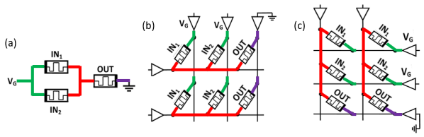
Several PIM technologies have been designed, including IMPLY (Borghetti et al., 2010) and MAGIC (Kvatinsky et al., 2014a) gates. MAGIC gates have become a commonly used PIM technology. Figure 1(a) shows the MAGIC NOR logic gate structure, where the two input memristors are connected to an operating voltage, , and the output memristor is grounded. Since MAGIC is a stateful logic family, the gate inputs and output are represented as memristor resistance. The input memristors are set with the input values of the logic gate and the output memristor is initialized at . The resistance of the output memristor changes during the execution according to the voltage divider rule, and switches when the voltage across it is higher than . The same gate structure can be used to implement an OR logic gate, with minor modifications (the output memristor is initialized at and a negative operating voltage is applied) (Hoffer et al., 2020). As depicted in Figures 1(b) and 1(c), a single MAGIC NOR gate can be mapped to a memristive crossbar array row (horizontal operation) or column (vertical operation). Multiple MAGIC NOR gates can operate on different rows or columns concurrently, thus enabling massive parallelism. Overall, logic is performed using the exact same devices that store the data.
2.4. Logic Execution within a Memristive Crossbar Array
A functionally complete memristive logic gate, e.g., a MAGIC NOR gate, enables in-memory execution of any logic function. The in-memory execution is performed by a sequence of operations performed over several clock cycles. In each clock cycle, one operation can be performed on a single row or column, or on multiple rows or columns concurrently, if the data is row-aligned or column-aligned. The execution of an arbitrary logic function with stateful logic has been widely explored in the literature (Tenace et al., 2019; Ben Hur et al., 2017; Ben-Hur et al., 2020; Yadav et al., 2019). Many execution and mapping techniques first use a synthesis tool, which synthesizes the logic function and creates a netlist of logic gates. Then, each logic gate in the netlist is mapped to several cells in the memristive crossbar and operated in a specific clock cycle. Each technique maps the logic function according to its algorithm, based on different considerations, e.g., latency, area, or throughput optimization.
Many techniques use several rows or columns in the memristive crossbar array for the mapping (Ben Hur et al., 2017; Tenace et al., 2019; Bhattacharjee et al., 2020) to reduce the number of clock cycles per a single function or to allow mapping of functions that are longer than the array row size by spreading them over several rows. The unique characteristic of the crossbar array, which enables parallel execution of several logic gates in different rows or columns, combined with an efficient cell reuse feature that enables condensing long functions into short crossbar rows, renders single instruction multiple data (SIMD) operations attractive. In SIMD operations, the same function is executed simultaneously on multiple rows or columns. Executing logic in SIMD mode increases the computation throughput; therefore, by limiting the entire function mapping to a single row or column, the throughput can be substantially improved. This is applied in the SIMPLER (Ben-Hur et al., 2020) mapper. Specifically, efficient cell reuse is implemented in SIMPLER by overwriting a cell when its old value is no longer needed. With cell reuse, SIMPLER can squeeze functions that require a long sequence of gates into short memory rows, e.g., a 128-bit addition that takes about 1800 memory cells without cell reuse is compacted into less than 400 memory cells with cell reuse. In this paper, we assume, without loss of generality, that a logic function is mapped into a single row in the memristive crossbar and cloned to different rows for different data.
2.5. The memristive Memory Processor Unit (mMPU) Architecture
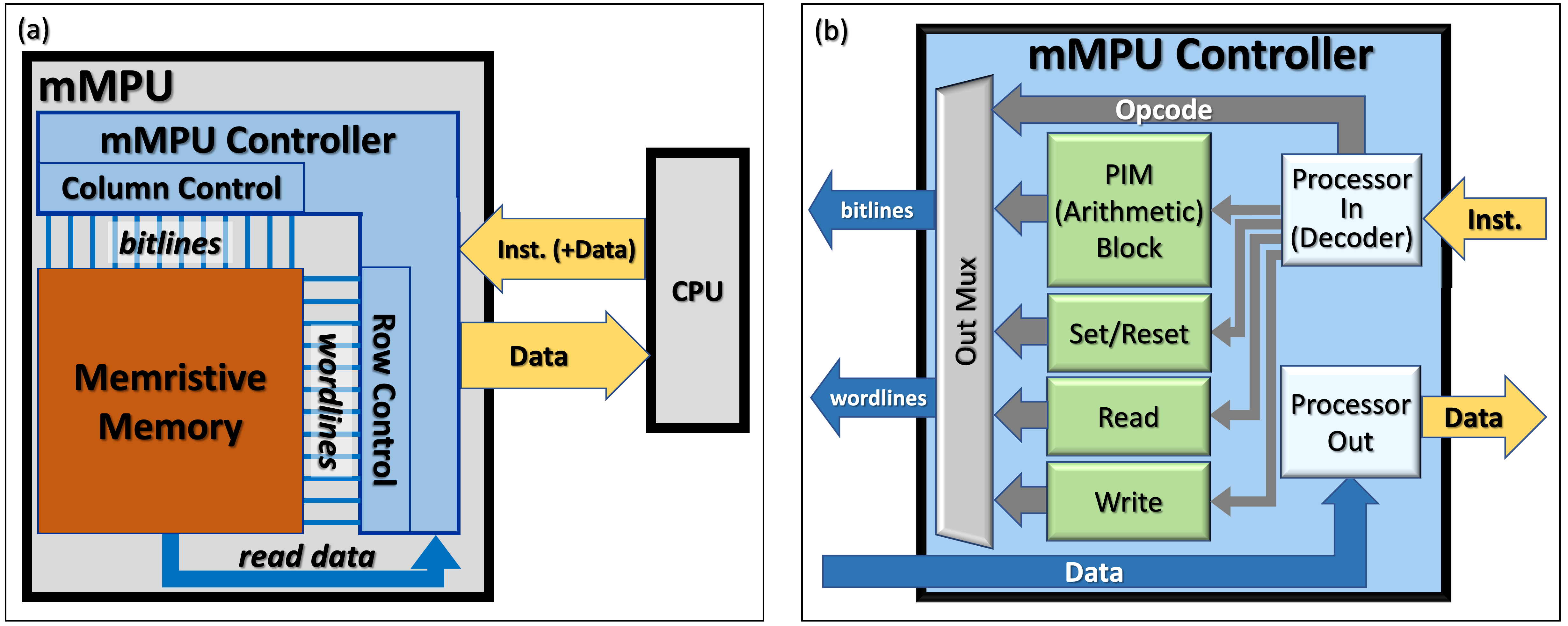
A PIM system requires a controller to manage its operation. In (Ben Hur and Kvatinsky, 2016), a design of a memristive memory processing unit (mMPU) controller is presented. Figure 2 depicts the mMPU architecture, as detailed in (Ben Hur and Kvatinsky, 2016). Figure 2(a) describes the interfaces between the mMPU controller, the memory, and the CPU. The CPU sends instructions to the mMPU controller, optionally including data to be written to memory. The mMPU processes each instruction and converts it into one or more memory commands. For each command, the mMPU determines the voltages applied on the wordlines and bitlines of the memristive memory arrays so that the command will be executed. Figure 2(b) depicts the internal structure of the mMPU controller. The instruction is interpreted by the decoder and then further processed by one of the green processing blocks according to the instruction type. The set of mMPU instruction types consists of the traditional memory instruction types: Load, Store, Set/Reset, and a new family of instructions: PIM instructions. Load and store instructions are processed in the read and write blocks, respectively. Initialization instructions are processed in the Set/Reset block. PIM instructions are processed in the PIM (”arithmetic”) block. The PIM block breaks each PIM instruction into a sequence of micro-instructions, and executes this sequence in consecutive clock cycles, as described in abstractPIM (Eliahu et al., 2020). The micro-instructions supported by the target mMPU controller can be easily adapted and modified according to the PIM technology in use, e.g., MAGIC NOR and IMPLY. Load instructions return data to the CPU through the controller via the data lines.
For PIM-relevant workloads, the overhead of the mMPU controller on the latency, power, and energy of the system is rather low. This is due to the fact that each PIM instruction operates on many data elements in parallel. Thus, the controller/instruction overhead is negligible relative to the latency, power, and energy cost of the data being processed within the memristive memory and the data transfer between memory and CPU (Talati et al., 2019).
3. PIM Use Cases and Computation Principles
After presenting the motivation for PIM in the previous section, in this section, we describe potential use cases of PIM. We start with a high-level estimate of the potential benefits of reduced data transfer. Later, we define some computation principles, and using them, we assess the performance cost of PIM computing.
3.1. PIM Use Cases and Data Transfer Reduction
As stated in Section 2, the benefit of PIM comes mainly from the reduction in the amount of the data transferred between the memory and the CPU. If the saved time and energy due to the data transfer reduction is higher than the added cost of PIM processing, then PIM is beneficial. In this sub-section, we list PIM use cases that reduce data transfer and quantify this reduction.
For illustration, assume our data reflect a structured database in the memory that consists of records, where each record is mapped into a single row in the memory. Each record consists of fields of varying data types. A certain compute task reads certain fields of each record, with an overall size of bits, and writes back (potentially zero) bits as the output. Define as the total number of accessed bits per record. Traditional CPU-based computation consists of transferring bits from memory to the CPU, performing the needed computations, and writing back bits to the memory. In total, these computations require the transfer of bits between the memory and the CPU. By performing all or part of the computations in memory, the total amount of data transfer can be reduced. This reduction is achieved by either reducing (or eliminating) the bits transferred per record (), and/or by reducing the number of transferred records ().
Several potential use cases follow, all of which differ in the way a task is split between PIM and CPU. In all cases, we assume that all records are appropriately aligned in the memory, so that PIM can perform the basic computations on all records concurrently (handling unaligned data is discussed later in Section 3.2). Figure 3 illustrates these use cases.

-
•
CPU Pure. This is the baseline use case. No PIM is performed. All input and output data are transferred to the CPU and back. The amount of data transferred is bits.
-
•
PIM Pure. In this extreme case, the entire computation is done in memory and no data is transferred. This kind of computation is done, for example, as a pre-processing stage in anticipation of future queries. See relevant examples under PIM Compact and PIM filter below.
-
•
PIM Compact. Each record is pre-processed in memory in order to reduce the number of bits to be transferred to the CPU from each record. For example, each product record in a warehouse database contains 12 monthly shipment quantity fields. The application only needs the yearly quantity. Summing (”Compacting”) these 12 elements into one reduces the amount of data transferred by 11 elements per record. Another example is an application that does not require the explicit shipping weight values recorded in the database, but just a short class tag (light, medium, heavy) instead. If the per-record amount of data is reduced from to bits, then the overall reduction is bits.
Table 1. PIM Use Cases Data Transfer Reduction Use Case Records Size Data Transferred Data Transfer Reduction -
–
/: overall/selected number of records; /: original/final size of records.
-
–
: bit-vector/list of indices; : all records/per XB
-
–
-
•
PIM Filter. Each record is processed in memory to reduce the number of records transferred to the CPU. This is a classical database query case. For example, an application looks for all shipments over $1M. Instead of passing all records to the CPU and checking the condition in the CPU, the check is done in memory and only the records that pass the check (”Filtering”) are transferred. If only out of records of size are selected, then the overall data transfer is reduced by bits. Looking deeper, we need to take two more factors into account:
(1) When the PIM does the filtering, the location of the selected records should also be transferred to the CPU, and the cost of transferring this information should be accounted for. Transferring the location can be done by either () passing a bit vector ( bits) or by () passing a list of indices of the selected records ( bits). The amount of the total data to be transferred is therefore . For simplicity, in this paper, we assume passing a bit vector (). The overall cost of transferring both the data and the bit vector is . The amount of saved data transfer relative to CPU Pure is bits.
(2) When filtering is done on the CPU only, data may be transferred twice. First, only a subset of the fields (the size of which is ) that are needed for the selection process are transferred, and only then, the selected records or a different subset of the records. In this CPU Pure case, the amount of transferred data is .
-
•
PIM Hybrid. This use case is a simple combination of applying both PIM Compact and PIM filter. The amount of data transferred depends on the method we use to pass the list of selected records, denoted above as or . For example, when using , the transferred data consists of records of size and a bit-vector of size bits. That is .
-
•
PIM Reduction. The reduction operator ”reduces the elements of a vector into a single result”333https://en.wikipedia.org/wiki/Reduction_Operator, e.g., computes the sum, or the minimum, or the maximum of a certain field in all records in the database. The size of the result may be equal to or larger than the original element size (e.g., summing a million of 8-bits arbitrary numbers requires 28 bits). ”Textbook” reduction, referred to later as , replaces elements of size with a single element of size (), thus eliminating data transfer almost completely. A practical implementation, referred to later as , performs the reduction on each memory array (XB) separately and passes all interim reduction results to the CPU for final reduction. In this case, the amount of transferred data is the product of the number of memory arrays used by the element size, i.e., , where is the number of records (rows) in a single XB.
Table 1 summarizes all use cases along with the amount of transferred and saved data. In this table, and reflect the overall and selected number of the transferred records. and reflect the original and final size of the transferred records.
3.2. PIM Computation Principles
Stateful logic-based PIM (or just throughout this paper) computation provides very high parallelism. Assuming the structured database example above (Section 3.1), where each record is mapped into a single memory row, PIM can generate only a single bit result per record per memory cycle (e.g., a single NOR, IMPLY, AND, based on the PIM technology). Thus, the sequence needed to carry out a certain computation may be rather long. Nevertheless, PIM can process many properly aligned records in parallel, computing one full column or full row per XB per cycle444The maximum size of a memory column or row may be limited in a specific PIM technology due to e.g., wire delays and write driver limitations.. Proper alignment means that all the input cells and the output cell of all records occupy the same column in all participating memory rows (records), or, inversely, the input cells and the output cell occupy the same rows in all participating columns.
PIM can perform the same operation on many independent rows, and many XBs, simultaneously. However, performing operations involving computations between rows (e.g., shift or reduction) or in-row copy of an element with a different alignment in each row, has limited parallelism. Such copies can be done in parallel among XBs, but within a XB, are performed mostly serially. When the data in a XB are aligned, operations can be done in parallel (as demonstrated in Figures 1(b) and 1(c) for row-aligned and column-aligned operations, respectively). However, operations on unaligned data cannot be done concurrently, as further elaborated in Section 3.2.
To quantify PIM performance, we first separate the computation task into two steps: Operation and Placement and Alignment. Below, we assess the complexity of each of these steps. For simplicity, we assume computations done on rows and memory arrays, i.e., .
Operation Complexity (). As described in Section 2.3, PIM computations are carried out as a series of basic operations, applied to the memory cells of a row inside a memristive memory array. While each row is processed bit-by-bit, the effective throughput of PIM is increased by the inherent parallelism achieved by simultaneous processing of multiple rows inside a memory array and multiple memory arrays in the system memory. We assume the same computations (i.e., individual operations) applied to a row are also applied in parallel in every cycle across all the rows () of a memory array.
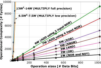
We define Operation Complexity () for a given operation type and data size, as the number of cycles required to process the corresponding data. Figure 4 shows how the input data length () affects the computing cycles for PIM-based processing. The figure shows that this number is affected by both the data size, as well as operation types (different operations follow a different curve on the graph). In many cases, is linear with the data size, for example, in a MAGIC NOR-based PIM, -bit AND requires cycles (e.g., for =16 bits, AND takes 16x3 = 48 cycles), while ADD requires 9 cycles555ADD can be improved to 7 cycles using four-input NOR gates instead of two-input NOR gates.. Some operations, however, are not linear, e.g., full precision MULTIPLY bits requires cycles (Haj-Ali et al., 2018) or approximately cycles, while low precision MULTIPLY bits requires about half the number of cycles, or approximately cycles. The specific Operation Complexity behavior depends on the PIM technology, but the principles are similar.
Placement and Alignment Complexity (). PIM imposes certain constraints on data alignment and placement (Talati et al., 2018). To align the data for subsequent row-parallel operations, a series of data alignment and placement steps, consisting of copying data from one place to another, may be needed. The number of cycles needed to perform these additional copy steps is captured by the placement and alignment complexity parameter, denoted as . Currently, for simplicity, we consider only the cost of intra-XB data copying, we ignore the cost of inter-XB data copying, and we assume that multiple memory arrays continue to operate in parallel and independently. Refining the model to account for inter-XB data copying will be considered in the future (see Section 6.5).
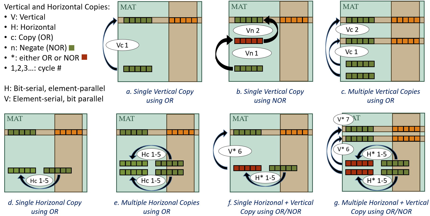
The PAC cycles required to copy the data in a memory array to the desired locations can be broken down into a series of horizontal row-parallel copies (), and vertical column-parallel copies (). Figure 5 shows examples of VCOPY and HCOPY operations involving copying a single element (Figures 5(a), 5(b), 5(d)) and multiple elements (Figures 5(c), 5(e), 5(f), 5(g)). HCOPYs and VCOPYs are symmetric operations: HCOPY can copy an entire memory column (or part of it) in parallel, while VCOPY can copy an entire memory row (or part of it) in parallel. Figure 5(g) depicts the case of copying column-aligned elements, each -bit wide (in green, =2, =5), into different rows to be placed in the same rows as other column aligned elements (in orange). First, HCOPYs are performed in a bit-serial, element-parallel, manner (copying elements from green to brown). In the first HCOPY cycle, all the first bits of all involved elements are copied in parallel. Then, in the second cycle, all the second bits of all involved elements are copied in parallel. This goes on for cycles until all bits in all elements are copied. Next, VCOPYs are performed in an element-serial, bit-parallel manner (copying from brown to green). In the first VCOPY cycle, all the bits of the first selected element are copied, in parallel, to the target row. Then, in the second cycle, all the bits of the second selected element are copied, in parallel. This goes on for cycles until all elements are copied.
When the involved data elements across different rows are not aligned, separate HCOPYs are performed individually for each data element, thus requiring additional cycles. A VCOPY for a given data element, on the other hand, can be done in parallel on all the bits in the element, which are in the same row. However, each row within a XB has to be vertically copied separately, in a serial manner.
The number of cycles it takes to perform a single bit copy (either HCOPY or VCOPY) depends on the PIM technology used. For example, MAGIC OR-based PIM technology ( (Hoffer et al., 2020)) supports logic OR as a basic operation, allowing a 1-cycle bit copy (see Figure 5(a), 5(c), 5(d), and 5(e)). PIM Technologies that do not support a 1-cycle bit copy (e.g., MAGIC NOR-based PIM technology), have to execute two consecutive NOT operations that take two cycles to copy a single bit (Figure 5(b)). However, copying a single bit using a sequence of a HCOPY operation followed by a VCOPY operation can be implemented as two consecutive OR or NOT operations that take two cycles regardless of the PIM technology used (Figure 5(f) and 5(g)).
We define Computation complexity () as the number of cycles required to fully process the corresponding data. equals the sum of and .
Below are examples of PIM cycles. We use the terms Gathered and Scattered to refer to the original layout of the elements to be aligned. Gathered means that all input locations are fully aligned among themselves, but not with their destination, while Scattered means that input locations are not aligned among themselves.
-
•
Parallel aligned operation. Adding two vectors, and , into vector , where , and are in row . The size of each element is -bits. A MAGIC NOR-based full adder operation takes cycles. Adding two -bit elements in a single row takes cycles. At the same cycles, one can add either one element or millions of elements. Since there are no vertical or horizontal copies, the equals the . The above-mentioned PIM Compact, PIM Filter, and PIM Hybrid use cases are usually implemented as parallel aligned operations.
-
•
Gathered placement and alignment copies. Assume we want to perform a shifted vector copy, i.e., copying vector into vector such that .666We ignore the elements of that are last in each XB. The size of each element is -bit. With stateful logic, the naive way of making such a copy for a single element is by a sequence of operations followed by operations. For a given single element in a row , first, copy all bits of in parallel, so , then, copy . Copying -bits in a single row takes cycles. As in the above parallel aligned case, in the same cycles, one can copy either one element or many elements. However, in this case, we also need to copy the result elements from one row to the adjacent one above. Copying -bits between two rows takes a single cycle, as all bits can be copied from one row to another in parallel. But, copying all rows is a serial operation, as it must be done separately for each row in the XB. Hence, if the memory array contains rows, the entire copy task will take cycles. Still, these operations can be done in parallel on all the XBs in the system. Hence, copying all elements can be completed in the same cycles.
-
•
Gathered unaligned operation. The time to perform a combination of the above two operations, e.g., , is the sum of both computations, that is cycles.
-
•
Scattered placement and alignment. We want to gather unaligned -bit elements into a row-aligned vector , that is, all elements occupy the same columns. Assume the worst case where all elements have to be horizontally and vertically copied to reach their desired location, as described above for Gathered placement and alignment. To accomplish this, we need to do horizontal 1-bit copies and one parallel -bit copy for each element, totaling overall cycles.
-
•
Scattered unaligned operation. Perform a Scattered placement and alignment followed by a parallel aligned operation, takes the sum of both computations, that is, cycles.
-
•
Reduction. We look at a classical reduction where the reduction operation is both commutative and associative (e.g., a sum, a minimum, or a maximum of a vector). For example, we want to sum a vector where each element, as well as the final sum, are of size , i.e., . The idea is to first reduce all elements in each XB into a single value separately, but in parallel, and then perform the reduction on all interim results. There are several ways to perform a reduction, the efficiency of which depends on the number of elements and the actual operation. We use the tree-like reduction777https://en.wikipedia.org/wiki/Graph_reduction, which is a phased process, in which at the beginning of each phase, we start with elements (, the number of rows, in the first phase), pair them into groups, perform all additions, and start a new phase with the -generated numbers. For elements, we need phases. Each phase consists of one parallel (horizontal) copy of bits, followed by serial (vertical) copies, and ending with one parallel operation (in our case, -bit add). The total number of vertical copies is . Overall, the full reduction of a single XB in all phases takes cycles. The reduction is done on all involved XBs in parallel, producing a single result per XB. Later, all per XB interim results are copied into fewer XBs and the process continues recursively over steps. Copying all interim results into fewer XBs and using PIM on a smaller number of XBs is inefficient as it involves serial inter-XB copies and low-parallel PIM computations. Therefore, for higher efficiency, after the first reduction step is done using PIM, all interim results are passed to the CPU for the final reduction, denoted as in Section 3.
| Computation type | Operate Row Parallel | HCOPY Row Parallel | VCOPY Row Serial | Total | Approximation |
| Parallel Operation | - | - | |||
| Gathered Placement & Alignment | - | ||||
| Gathered Unaligned Operation | |||||
| Scattered Placement & Alignment | - | ||||
| Scattered Unaligned Operation | |||||
-
•
: Operation Complexity, : Width of element, : Number of rows, : Number of reduction phases.
Table 2 summarizes the computation complexity in cycles of various PIM computation types (ignoring inter-XB copies, as mentioned above). Usually, and , so is approximately , and and are approximately . The last column in the table reflects this approximation. The approximation column hints to where most cycles go, depending on , , and . Parallel operations depend on only and are independent of , the number of elements (rows). When placement and alignment take place, there is a serial part that depends on and is a potential cause for computation slowdown.
4. PIM and CPU Performance
In the previous section, the PIM use cases and computation complexity were introduced. In this section, we devise the actual performance equations of PIM, CPU, and combined PIM+CPU systems.
4.1. PIM Throughput
represents the time it takes to perform a certain computation, similar to the latency of an instruction in a computing system. However, due to the varying parallelism within the PIM system, does not directly reflect the PIM system performance. To evaluate the performance of a PIM system, we need to find its system throughput, which is defined as the number of computations performed within a time unit. Common examples are Operations Per Second (OPS) or Giga Operations per Second (GOPS). For a PIM Pure case, when completing computations takes time, the PIM throughput is:
| (1) |
To determine , we obtain the PIM and multiply it by the PIM cycle time ()888We assume that the controller impact on the overall PIM latency is negligible, as explained in Section 2.5.. depends on the specific PIM technology used. To compute , we use the equations in Table 2. The number of computations is the total number of elements participating in the process. When single-row based computing is used, this number is the number of all participating rows, which is the product of the number of rows within a XB with the number of XBs, that is, . The PIM throughput is therefore
| (2) |
For example, consider the Gathered unaligned operation case for computing shifted vector-add, . Assuming cycles (-bit add), element size bits, rows, and memory arrays, then elements. cycles. The number of cycles to compute elements also equals the time to compute elements and is or cycles. The PIM throughput per cycle is computations per cycle. The throughput is computations per time unit. We can derive the throughput per second for a specific cycle time. For example, for a of 10ns, the PIM throughput is OPS GOPS.
In the following sections, we explain the CPU Pure performance and throughput and delve deeper into the overall throughput computation when both PIM and CPU participate in a computation.
4.2. CPU Computation and Throughput
Performing computation on the CPU involves moving data between the memory and the CPU (Data Transfer), and performing the actual computations (e.g., ALU Operations) within the CPU core (CPU Core). Usually, on the CPU side, Data Transfer and CPU Core Operations can overlap, so the overall CPU throughput is the minimum between the data transfer throughput and the CPU Core Throughput.
Using PIM to accelerate a workload is only justified when the workload performance bottleneck is the data transfer between the memory and the CPU, rather than the CPU core operation. In such workloads, the data-set cannot fit in the cache as the data-set size is much larger than the CPU cache hierarchy size. Cases where the CPU core operation, rather than the data transfer, is the bottleneck, are not considered PIM-relevant. In PIM-relevant workloads, the overall CPU throughput is dominated by the data transfer throughput.
The data transfer throughput depends on the memory to CPU bandwidth and the amount of data transferred per computation. We define as the memory to CPU bandwidth in bits per second (bps), and () as the number of bits transferred for each computation. That is:
| (3) |
We demonstrate the data transfer throughput using, again, the shifted 16-bit vector-add example. In Table 3, we present three interesting cases, differing in their size. (a) CPU Pure. The two inputs and the output are transferred between the memory and the CPU (. (b) Inputs only. Same as CPU Pure, except that only the inputs are transferred to the CPU; no output result is written back to memory (. (c) Compaction. Where PIM performs the add operation and passes only the output data to the CPU for further processing (. We use the same data bus bandwidth, GOPS, for all three cases. Note that the data transfer throughput depends only on the data sizes, it is independent of the operation type. The throughput numbers in the table reflect any binary 16-bit operation, either simple as OR or complex as divide. The table hints at the potential gain that PIM opens by reducing the amount of data transfer between the memory and CPU. If PIM throughput is sufficiently high, the data transfer reduction may compensate for the additional PIM computations and the combined PIM+CPU system throughput may exceed the throughput of a system using the CPU only with PIM.
Special care must be taken when determining DIO for the PIM Filter and PIM Reduction cases since only a subset of the records are transferred to the CPU. Note that the DIO parameter reflects the number of data bits transferred per accomplished computation, even though the data for some computations were not eventually transferred. In these cases, the DIO should be set as the total number of transferred data bits divided by the number of computations done in the system. For example, assume a filter, where we process records of size , and pass only of them (). The DIO, in case we use a bit-vector to identify chosen records, is . e.g., if and , DIO is bits. That is, the amount of data transfer per computation went from 200 to 3 bits per computation, i.e., reduction. The data transfer throughput for the filter case is presented in Table 3.
| Computation type | Bandwidth (BW) [Gbps] | DataIO (DIO) [bits] | Data Transfer Throughput () [GOPS] |
| CPU Pure | 1000 | 48 | 20.8 |
| Inputs Only | 1000 | 32 | 31.3 |
| Compaction | 1000 | 16 | 62.5 |
| Filter (200 bit, 1%) | 1000 | 3 | 333.3 |
4.3. Combined PIM and CPU Throughput
In a combined PIM and CPU system, achieving peak PIM throughput requires operating all XBs in parallel, thus preventing overlapping PIM computations with data transfer999Overlapping PIM computation and data transfer can be made possible in a banked PIM system. See Pipelined PIM and CPU in Section 6.5.. In such a system, completing computations takes PIM time and data transfer time, and the combined throughput is, by definition:
| (4) |
Fortunately, computing the combined throughput does not require knowing the values of and . can be computed using the throughput values of its components, and , as follows:
| (5) |
Since the PIM and CPU operations do not overlap, the combined throughput is always lower than the throughput of each component for the pure cases with the same parameters. For example, in the Gathered unaligned operation case above, when computing a 16-bit shifted vector-add, i.e., , we do the vector-add in PIM, and transfer the 16-bit result vector to the CPU (for additional processing). We have already shown that, for the parameters we use, the PIM Throughput is GOPS, and the data transfer throughput is GOPS. Using Eq. (5), the combined throughput GOPS, which is indeed lower than 160 and 62.5 GOPS. However, this combined throughput is higher than that of the CPU Pure throughput using higher =32 or =48 (31.3 or 20.8 GOPS) presented in the previous subsection. Of course, these results depend on the specific parameters used here. A comprehensive analysis of the performance sensitivity is described in Section 6.2.
5. Power and Energy
When evaluating the power and energy aspects of a system, we examine two factors:
-
•
Energy per computation. The energy needed to accomplish a single computation. This energy is determined by the amount of work to be done (e.g., number of basic operations) and the energy per operation. Different algorithms may produce different operation sequences thus affecting the amount of work to be done. Physical characteristics of the system affect the energy per operation. Energy per Computation is a measure of system efficiency. A system configuration that consumes less energy per a given computation is considered more efficient. For convenience, we generally use Energy Per Giga Computations. Energy is measured in Joules.
-
•
Power. The power consumed while performing a computation. The maximum allowed power is usually determined by physical constraints like power supply and thermal restrictions, and may limit system performance. It is worth noting that the high parallel computation of PIM causes the memory system to consume much more power when in PIM mode than when in standard memory load/store mode. Power is measured in Watts (Joules per second).
In this section, we evaluate the PIM, the CPU, and the combined system power and energy per computation and how it may impact system performance. For the sake of this coarse-grained analysis, we consider dynamic power only and ignore power management and dynamic voltage scaling.
5.1. PIM Power and Energy
Most power models target a specific design. The below approach is more general and resembles the one used for floating-point add/multiply power estimation in FloatPIM (Imani et al., 2019). In this approach, every PIM operation consumes energy. For simplicity, we assume that in every PIM cycle, the switching of a single cell consumes a fixed energy . This is the average amount of energy consumed by each participating bit in each XB, and accounts for both the memristor access as well as other overheads such as the energy consumed by the wires and the peripheral circuitry connected to the specific bitline/wordline101010We assume that the controller impact on the overall PIM power and energy is negligible, as explained in Section 2.5.. The PIM energy per computation is the product of by the number of cycles . The PIM power is the product of the energy per computation by the PIM throughput (see Section 4.1).
| (6) | |||
| (7) |
5.2. CPU Power and Energy
Here we compute the CPU energy per computation and the power . As in the performance model, we ignore the actual CPU Core operations and consider only the data transfer power and energy. Assume that transferring a single bit of data consumes . Hence, the CPU energy per computation is the product of by the number of bits per computation . The CPU power is simply the product of the energy per computation with the CPU Throughput . When the memory to CPU bus is not idle, the CPU power is equal to the product of the energy per bit with the number of bits per second, which is the memory to CPU bandwidth .
| (8) | |||
| (9) |
If the bus is busy only part of the time, the CPU power should be multiplied by the relative time the bus is busy, that is, the bus duty cycle,
5.3. Combined PIM and CPU Power and Energy
When a task is split between PIM and CPU, we treat them as if part of each computation is partly done on the PIM and partly on the CPU (see Section 4.3). The combined energy per computation is the sum of the PIM energy per computation and the CPU energy per computation . The overall system power is the product of the combined energy per computation and the combined system throughput:
| (10) | |||
| (11) |
Since PIM and CPU computations do not overlap, their duty cycle is less than 100%. Therefore, the PIM power in the combined PIM+CPU system is lower than the maximum PIM Power in a Pure PIM configuration. Similarly, the CPU Power in the combined PIM+CPU system is lower than the maximum CPU Power.
In order to compare energy per computation between different configurations, we use the relevant values, computed by dividing the power of the relevant configuration by its throughput. That is:
| (12) |
The following example summarizes the entire power and energy story. Assume, again, the above shifted vector-add example using the same PIM and CPU parameters. In addition, we use pJ (Lanza et al., 2019) and pJ (O’Connor et al., 2017). The PIM Pure throughput is 160 GOPS (see Section 4.1) and the PIM Pure power is W. The CPU Pure throughput (using Gpbs) is 20.8 (or 62.5) GOPS for 48 (or 16) bit DIO (see Section 4.2). The CPU Pure Power is 15*10W. A combined PIM+CPU system will exhibit throughput of GOPS and power W.
Again, these results depend on the specific parameters in use. However, they demonstrate a case where, with PIM, not only the system throughput went up, but, at the same time, the system power decreased. When execution time and power consumption go down, energy goes down as well. In our example, J/OP J/GOP, and J/OP J/GOP.
5.4. Power-Constrained Operation
Occasionally, a system, or its components, may be power-constrained. For example, using too many XBs in parallel, or fully utilizing the memory bus may exceed the maximum allowed system or component thermal design power111111https://en.wikipedia.org/wiki/Thermal_design_power (). For example, the PIM power must never exceed . When a system or a component exceeds its , it has to be slowed down to reduce its throughput and hence, its power consumption. For example, a PIM system throughput can be reduced by activating fewer XBs or rows in each cycle, increasing the cycle time, or a combination of both. CPU power can be reduced by forcing idle time on the memory bus to limit its bandwidth (i.e., ”throttling”).
6. The Bitlet Model - Putting it All Together
So far, we have established the main principles of the PIM and CPU performance. In this section, we first present the Bitlet model itself, basically summarizing the relevant parameters and equations to compute the PIM, CPU, and combined performance in terms of throughput. Then, we demonstrate the application of the model to evaluate the potential benefit of PIM for various use cases. We conclude with a sensitivity analysis studying the interplay and impact of the various parameters on the PIM and CPU performance and power.
6.1. The Bitlet Model Implementation
The Bitlet model consists of ten parameters and nine equations that define the throughput, power, and energy of the different model configurations. Table 4 summarizes all Bitlet model parameters. Table 5 lists all nine Bitlet equations.
PIM performance is captured by six parameters: , , , , and . Note that and are just auxiliary parameters used to compute . CPU performance is captured by two parameters: and . PIM and CPU energy are captured by the and the parameters. For conceptual clarity and to aid our analysis, we designate three parameter types: technological, architectural, and algorithmic. Typical values or ranges for the different parameters are also listed in Table 4. The table contains references for the typical values of the technological parameters , , and , which are occasionally deemed controversial. The model itself is very flexible, it accepts a wide range of values for all the parameters. These values do not even need to be implementable and can differ from the parameters’ typical values or ranges. This flexibility allows limit-studies by modeling systems using extreme configurations.
The nine Bitlet model equations determine the PIM, CPU and the combined performance (, , ), power (, , ), and energy per computation (, , ).
| Parameter name | Notation | Typical Value(s) | Type |
| PIM operation complexity | 1 - 64k cycles | Algorithmic | |
| PIM placement and alignment complexity | 0 - 64k cycles | Algorithmic | |
| PIM computational complexity | 1 - 64k cycles | Algorithmic | |
| PIM cycle time | 10 ns (Lanza et al., 2019) | Technological | |
| PIM array dimensions (rows columns) | 16x16 - 1024x1024 | Technological | |
| PIM array count | 1 - 64k | Architectural | |
| PIM energy for operation (=1) per bit | 0.1pJ (Lanza et al., 2019) | Technological | |
| CPU memory bandwidth | 0.1 - 16 Tbps | Architectural | |
| CPU data in-out bits | 1 - 256 bits | Algorithmic | |
| CPU energy per bit transfer | 15pJ (O’Connor et al., 2017) | Technological |
| Entity | Equation | Units |
| PIM Throughput | GOPS | |
| CPU Throughput | GOPS | |
| Combined Throughput | GOPS | |
| PIM Power | Watts | |
| CPU Power | Watts | |
| Combined Power | Watts | |
| PIM Energy per Computation | J/GOP | |
| CPU Energy per Computation | J/GOP | |
| Combined Energy per Computation | J/GOP |
6.2. Applying The Bitlet Model
The core Bitlet model is implemented as a straightforward Excel spreadsheet121212The spreadsheet is available at https://asic2.group/tools/architecture-tools/. All parameters are inserted by the user and the equations are automatically computed. Figure 6 is a snapshot of a portion of the Bitlet Excel spreadsheet that reflects several selected configurations.
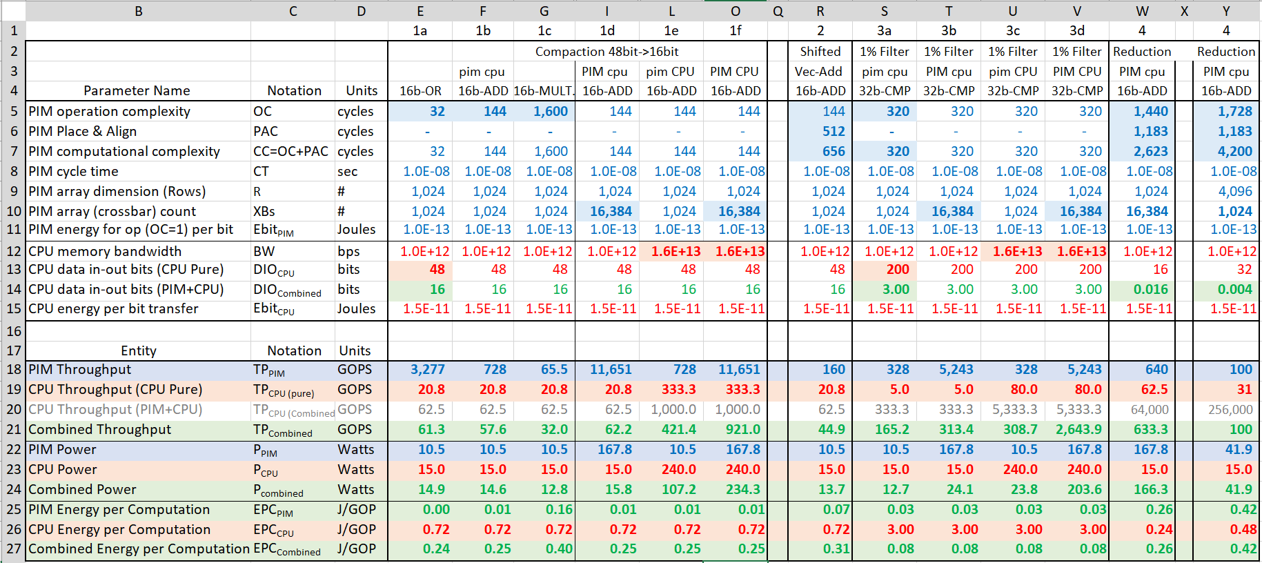
Few general notes:
-
•
The spreadsheet can include many configurations, one per column, simultaneously, allowing a wide view of potential options to ease comparison.
-
•
For convenience, in each column, the model computes the three related PIM Pure (PIM), CPU Pure (CPU), and the Combined configurations. To support this, the two DIO parameters are needed; one, , for the CPU Pure system, and one (usually lower), , for the combined PIM+CPU system. See rows 13-14 in the spreadsheet.
- •
-
•
Fonts and background are colored based on the system they represent: blue for PIM, green for CPU, and red for combined PIM+CPU system.
-
•
Bold parameter cells with a light background mark items highlighted in the following discussions and are not inherent to the model.
Following is an in-depth dive into the various selected configurations.
Compaction. Cases 1a-1f (columns E-O) describe simple parallel aligned operations. In all these cases, the PIM performs a 16-bit binary computation in order to reduce data transfer between the memory and the CPU from 48 bits to 16 bits. The various cases differ in the operation type (OR/ADD/MULTIPLY, columns E-G), the PIM array count (1024/16384 XBs), and the CPU memory bandwidth (1000/16000 Gpbs) see cases 1b, 1d-1f, rows 4, 10 and 12. Note that in row 3, ”pim” means a small PIM system (1024 XBs) while ”PIM” mean a large PIM system (16384 XBs). Same holds for ”cpu” (1Tbs) and ”CPU” (16Tbs). In each configuration, we are primarily interested in the difference between the CPU and the combined PIM+CPU system results. Several observations:
-
•
A lower (row 5) yields higher PIM throughput and combined PIM+CPU system throughput. The combined PIM+CPU system provides a significant benefit over CPU for OR and ADD operations, yet almost no benefit for MULTIPLY.
-
•
When the combined throughput is close to the throughput of one of its components, increasing the other component has limited value (e.g., in case 1d, using more XBs (beyond 1024) has almost no impact on the combined throughput (61 GOPS), as the maximum possible throughput with the current bandwidth (1000 Gbps) is 62 GOPS).
-
•
When the throughput goes up, so does the power. Using more XBs or higher bandwidth may require higher power than the system . Power consumption of over 200 Watts is likely too high. Such a system has to be slowed down by activating fewer XBs, enforcing idle time, etc…
-
•
A comparison of the PIM throughput and the CPU throughput (row 18 and 20) provides a hint as to how to speed up the system. Looking at case 1b (column F), the PIM throughput is 728 GOPS while the CPU throughput is 63 GOPS. In this case, it makes more sense to increase the CPU throughput, and indeed, case 1e (row 21, column L), which increases the CPU bandwidth, improves the throughput more than case 1d (column I) does.
Shifted Vector-add. Case 2 (column R) summarizes the example that was widely used in Sections 4.1 , 4.3 and 5.3.
Filter. Case 3a-3d (columns S-V) repeats the example in Section 4.2. It describes a filter that eventually selects 1% of the records and passes a bit-vector to identify the selected items. Each record is of bits. As in the compaction case above, the four configurations differ in their memory array size and the memory . Similar to the compaction case, we can get an idea of how to speed up the system by looking at rows 18 and 20. In this case, the PIM throughput is lower and it makes sense to add more XBs and not memory . Indeed, case 3b (column T) with stronger PIM, exhibits higher throughput than case 3c (column U) with higher memory .
Reduction. Case 4 (column W) reflects summing all elements in a 16-bit vector. For simplicity, we use the per-XB reduction method, , where all initial per-XB results are transferred to the CPU. On the CPU side, this computation is like a filter where only one element per XB () is transferred, and there is no need to transfer a bit-vector. On the PIM side, is determined as described in Table 2. With rows, the number of phases is . Overall, the of the reduction is relatively high, therefore, a PIM-based reduction solution requires many XBs to be more beneficial than a Pure CPU solution.
6.3. Impact and Interplay among Model Parameters
In the previous sub-section, we showed how to determine the throughput and the power of a given system configuration. Now we want to illustrate the sensitivity of the throughput and power to changes in different parameters. In this discussion, due to limited space and limited ability to visualize many parameters concurrently, we focus on the algorithmic and the architectural parameters only, i.e., and on the PIM side and and on the CPU side. The model itself, as illustrated in Figure 6, supports manipulation of all parameters.
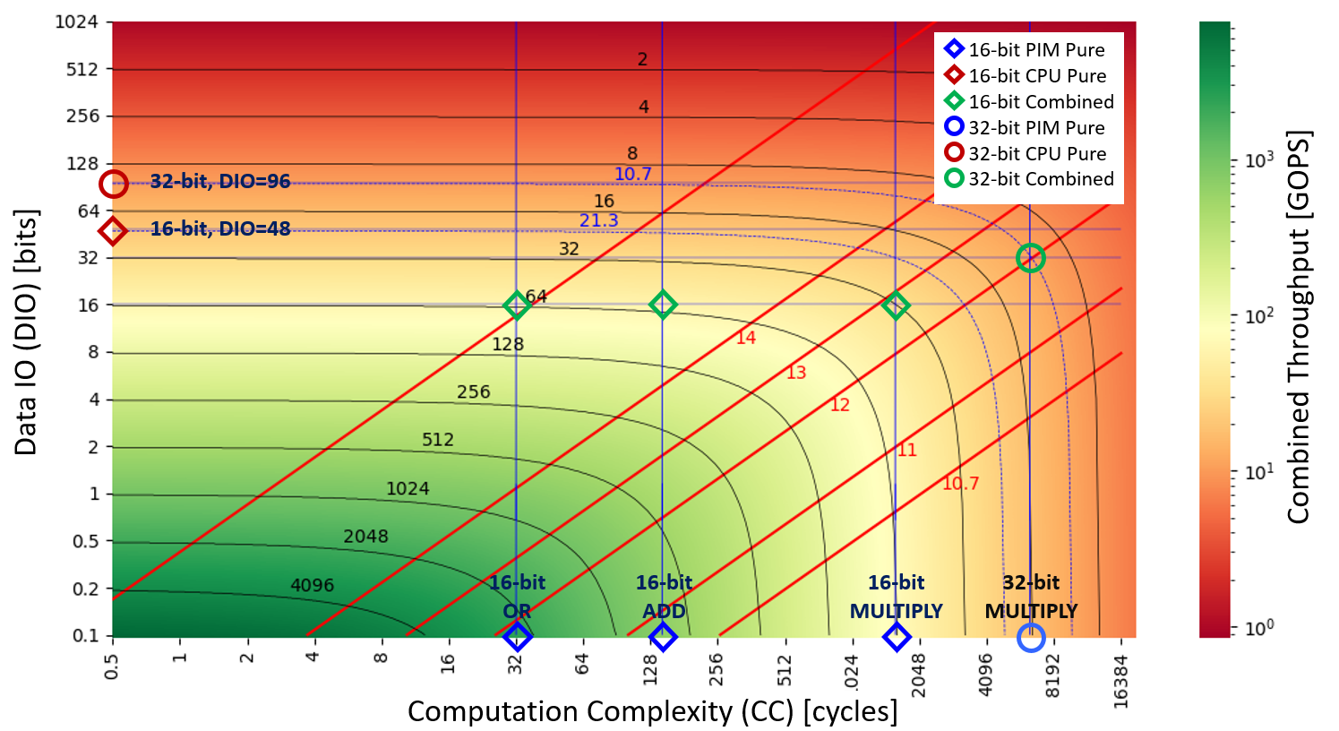
Fixed Parameters: arrays, rows, Gpbs, ns, pJ, pJ.
First, in Figure 7, we present the PIM, the CPU, and the combined PIM+CPU throughput and power as a function of and for a certain PIM and CPU configuration, where and Gbps. The color on the graph at point indicates the combined PIM+CPU throughput value when PIM and CPU . The black curved lines on the graph are equal throughput lines and are annotated with the throughput value in Gpbs. Points below a line have higher throughput and vice-versa. The throughput value at the point (, ) reflects the PIM Pure throughput when . The throughput value at the point (, ) reflects the CPU Pure throughput when . Note that since the axes are in logarithmic scales, the points where or do not appear on the graph but can be approximated by looking at the value of the equal throughput line that is close to it. For example, the PIM Pure throughput for is approximately 512 GOPS. Blue horizontal (vertical) lines are equal () lines to allow comparison between PIM, CPU, and Combined throughput. Red curved lines on the graph are equal power lines; in this graph, power goes up when going from bottom right to top left. Several points were highlighted on the graph. Diamond-shaped points represent the three 16-bit operations (OR/ADD/MULTIPLY) mentioned in the previous sub-section (cases 1a-1c in Figure 6). The circle-shaped points represent the 32-bit MULTIPLY operation. The relevant operation is marked above the relevant diamond on the axis. Observing marks with the same shape and operation type allows throughput comparison of the same operation between all three PIM, CPU, and combined PIM+CPU configurations. Observations:
-
•
For the same , higher implies lower throughput.
With higher , PIM benefits decline, e.g., PIM 32/64 bit MULTIPLY has same/lower throughput than CPU. -
•
For the same , higher implies lower throughput.
-
•
An equal throughput (black) line has a knee. On the left of the knee, the throughput is impacted mostly by , that is, the CPU is the bottleneck in this region. Below the knee, the throughput is impacted mostly by , i.e., the PIM is the bottleneck in this region.
-
•
For a given case, it is worth looking at three points:
(1) , representing the PIM Pure throughput,
(2) , representing the CPU Pure throughput,
(3) , representing the combined PIM+CPU system throughput. -
•
The equal power (red) lines reveal three power regions. The top left reflects the CPU bottle-necked region, where the power is very close to CPU Pure power. The bottom right reflects the PIM bottle-necked region, where the power is very close to PIM Pure power. The power changes mainly around the knee, where each small move to the left changes the power closer to the CPU Pure power and, similarly, each small move down changes the power closer to the PIM Pure power. In the current configuration ( , Gpbs ), where CPU Pure power is higher than PIM Pure power, left means higher power and down means lower power. Different configurations may exhibit different behaviors.
-
•
The linear behavior of the power lines reflects the fact that the combined PIM+CPU system power is a linear combination of the PIM Pure and CPU Pure power, where each is weighted according to the share of time they are active. When we multiply and by the same number, the time ratio remains the same, and so does the combined power.
Table 6 lists the marked points in the graph. The 64-bit MULTIPLY was added to the table to highlight a high computation complexity case where CPU Pure performs better than the combined PIM+CPU configuration.
| Operation | 16-bit OR | 16-bit ADD | 16-bit MULTIPLY | 32-bit MULTIPLY | 64-bit MULTIPLY |
| CC [cycles] | 32 | 144 | 1600 | 6400 | 25600 |
| DIO CPU / Combined [bits] | 48 / 16 | 48 / 16 | 48 / 16 | 96 / 32 | 192 / 64 |
| PIM Throughput [GOPS] | 3277 | 728 | 65.5 | 16.4 | 4.1 |
| CPU Throughput [GOPS] | 20.8 | 20.8 | 20.8 | 10.4 | 5.2 |
| Combined Throughput [GOPS] | 61.3 | 57.6 | 32.0 | 10.7 | 3.2 |
| PIM Power [Watts] | 10.5 | ||||
| CPU Power [Watts] | 15.0 | ||||
| Combined Power [Watts] | 14.9 | 14.6 | 12.8 | 12 | 11.4 |
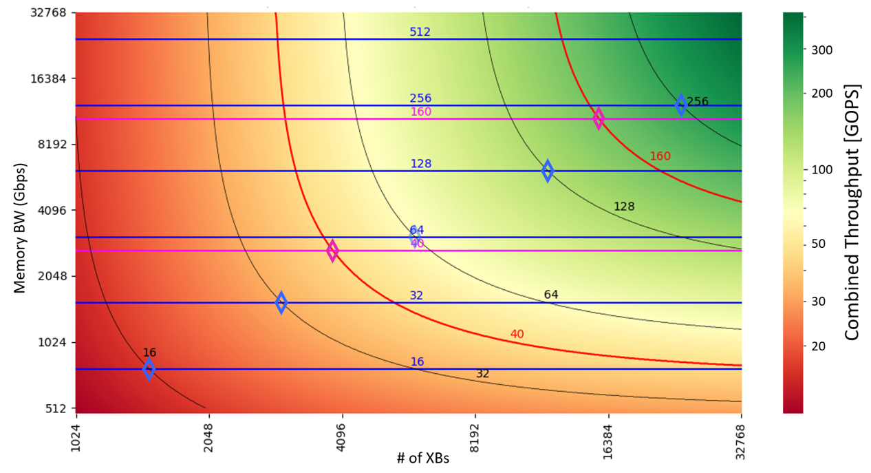
Fixed parameters: cycles, rows, bits, ns, pJ, pJ.
Finally, Figure 8 presents the impact of and on throughput and power. This figure assumes a certain pre-defined =6400 bits, =16 bits, and =48bits. The color on the graph at point indicates the combined PIM+CPU throughput value when PIM and CPU . The figure has curved and horizontal equal throughput and power lines. Black curved equal throughput lines and magenta curved equal power lines reflect the combined PIM+CPU configuration using =16 bits. Blue horizontal lines reflect the CPU Pure throughput, Magenta horizontal lines reflect the CPU Pure power, both at =48 bits. The diamond marks indicate throughput and power crossover points between natural trade-offs of Pure CPU at =48 bits and combined PIM+CPU at =16 bits. Observations:
-
•
Both throughput and power increase linearly when either or increase. The crossover points help compare the CPU Pure and combined PIM+CPU alternatives. When is high and is low, the PIM becomes the bottleneck and using CPU Pure is more beneficial than using PIM. On the other hand, when is low and is high, the combined PIM+CPU configuration is better.
-
•
The choice of working points out of all points on the same equal throughput or power line depends on the available technology and possible configurations. Bandwidth, memory size, or power limitation leaves only part of the space available, e.g., if is limited to 4000 Gbps and memory size is limited to 8192K , then roughly only points from the bottom left quarter of the graph are valid. If we also limit the power to 40 Watts, another part of the space becomes invalid.
-
•
We can model a PIM Pure system, by adding vertical lines to reflect PIM Pure power and performance (lines are not shown).
The above are just several examples of the types of analyses that are enabled by the Bitlet model. The model enables analytic exploration of many parameter combinations of PIM and CPU systems.
6.4. Analysis of Real-Life Examples using the Bitlet Model
In the previous sections, we analyzed relatively simple and synthetic examples. In this subsection, we apply the Bitlet model on several real-life examples taken from two PIM-related papers, the Fixed Point Dot Product (FiPDP), the Hadamard Product, and the Image Convolution from the IMAGING paper (Haj-Ali et al., 2018) and the Floating Point multiplication and addition from the FloatPIM paper (Imani et al., 2019). All examples map useful and important algorithms onto a MAGIC-based PIM system.
In all examples, the authors made an admirable effort to compute the latency and tried to assess the throughput and power of these computations. In most cases, the authors used a single configuration (, ), assumed a single value for the technological parameters, and deduced the throughput, power, and energy based on the single values.
The Bitlet model complements the above works nicely. Using their values for , the model can easily illustrate the throughput, power, and energy for different parameters. The model can help compare the results to the CPU Pure and the combined PIM+CPU systems.
6.4.1. IMAGING
The IMAGING paper (Haj-Ali et al., 2018) implements several algorithms and analyzes them, but does not consider technological parameters, e.g., cycle time and energy, in the analysis. As a consequence, it presents results in throughput per cycle and determines area based on the number of memory cells.
-
•
Fixed Point Dot Product (FiPDP)131313https://en.wikipedia.org/wiki/Dot_product. FiPDP is a classical dot-product , where two vectors are multiplied element-wise, and the result vector is summed. Assume two 8-bit vectors producing 16-bit interim results that are summed into 32-bit numbers. The paper assumes . The of the algorithm, as implemented in the IMAGING paper, consists of the multiplication step ( cycles) followed by the tree-like reduction step ( cycles). The two steps together take approximately cycles. The paper neither states the throughput of this operation nor does it make any sensitivity analysis. Using the Bitlet model, we can easily compute the throughput and analyze its sensitivity. For example, for , , and , we achieve PIM Pure and combined PIM+CPU throughput of about GOPS, which is rather low compared to the CPU Pure throughput of GOPs at Gpbs. Using a configuration of and increases the PIM Pure (and combined PIM+CPU) throughput to about GOPS, which is higher than the CPU Pure throughput of GOPS stated above.
-
•
Hadamard Product141414https://en.wikipedia.org/wiki/Hadamard_product_(matrices). The Hadamard Product is an element-wise matrix product, that is, for all , . In fact, it is equivalent to an element-wise vector product, that is, for all , . The paper focuses on 8-bit pixels as the elements to multiply. If memory space is scarce, several pairs of elements are located in the same row to fit the matrices in the available memory. The paper also considers the case where the input vectors are larger than the size of available memory, so the computation needs to be repeated. None of these manipulations affect the computation throughput since they result in doing, e.g., more work in longer time. For throughput computation, we use the Bitlet model assuming a single multiplication in each row. Doing so, we can obtain the real throughput in GOPS and compare it to the CPU Pure and the combined PIM+CPU system throughput.
Table 7 provides several examples with varying and values. We assume the paper’s original value of cycles. We use the Bitlet model to also compute the PIM Pure, CPU Pure, and combined PIM+CPU system throughput. For the CPU configuration, we assume Gbps, bits for CPU Pure, and bits for the combined system. As expected, the throughput goes up with the number of (and ). For low numbers of and , CPU Pure is better than a combined PIM+CPU system ( GOPS vs. GOPS). However, adding XBs improves the combined PIM+CPU system throughput compared to CPU Pure, providing over GOPS vs. GOPS, respectively.
Table 7. Throughput of the Hadamard Product [Cycles] [GOP/Cycle] [GOPS] [GOPS] [GOPS] 512 512 710 369 37 31 23 1,024 512 710 738 74 31 34 4,096 1,024 710 5,907 591 31 57 16,384 1,024 710 23,630 2,363 31 61 -
•
Image Convolution151515https://en.wikipedia.org/wiki/Kernel_(image_processing). A single convolution computation consists of multiplying a pixel window in a picture with a coefficient matrix and creating a new picture where the center element of the selected window is set with the newly computed value. is usually a small odd number, e.g., 3 or 5. Each pixel is -bits wide. The IMAGING paper goes a long (and smart) way to implement the convolution on top of the MAGIC NOR memory array and computing its latency. For our discussion, we need to consider only the following: (a) Computing each pixel involves -bit multiplications, () -bit additions, HCOPY operations and () VCOPY operations. The last pixels in each row (e.g., 1 or 2 pixels for ) are duplicated at the beginning of the next row. Therefore, to reduce space overhead, each row has to have a minimal number of pixels. In the aforementioned examples, pixels per row for and for . Table 8 lists the for convolutions using bits, and . The table clearly shows that convolution has a very high computation complexity.
Table 8. Convolution Computation Complexity. () [Cycles] () [Cycles] 3 69,296 77,488 5 188,592 204,976 At this point, we can use the Bitlet model and obtain the throughput values. One immediate observation is that since the input and output matrices have the same size, there is no data transfer reduction, and the value of using PIM as a pre-processing stage is questionable. In other words, both =16 and =16, thus the CPU Pure throughput is higher than that of the combined PIM+CPU throughput. We ignore this concern and compare PIM Pure to CPU Pure. Results are shown in Table 9. The table shows that convolution is significantly heavier than the previous examples examined above. This is expected, as convolution involves many multiplications per pixel, especially when . According to the model, only a huge PIM configuration () may compete with CPU Pure. One may question even that, since the power needed for this configuration, obtained from the Bitlet model as well, is approximately Watts. It is worth noting that this computation is quite heavy for the CPU core as well. Every pixel requires (for ) =9 8-bit multiplications and -1=8 16-bit additions, so to sustain convolutions per second, the CPU needs to perform about instructions per second. Achieving that throughput requires, for example, four 4-GHz high end CPUs, supporting two wide SIMD instructions (e.g., AVX-512161616https://en.wikipedia.org/wiki/AVX-512) per cycle.
Table 9. Convolution Throughput. [Cycles] [GOP/Cycle] [GOPS] [GOPS] [GOPS] 3 1,024 1,024 77,488 14 1.4 63 1.3 3 8,192 1,024 77,488 108 10.8 63 9.2 3 65,536 1,024 77,488 866 86.6 63 36.3 5 1,024 1,024 204,976 5 0.5 63 0.5 5 8,192 1,024 204,976 41 4.1 63 3.8 5 65,536 1,024 204,976 327 32.7 63 21.5
6.4.2. FloatPIM
The FloatPIM paper implements a fully-digital scalable PIM architecture that natively supports floating-point operations. As opposed to the IMAGING paper, FloatPIM does address time and power evaluation. In this section, we discuss the in-memory floating-point operation used in FloatPIM.
A floating-point multiply operation takes cycles, where and are the number of mantissa and exponent bits, respectively. Similarly, floating-point add operation takes NOR cycles and search cycles. For simplicity, we assume here that NOR and search cycles have the same cycle time. The paper uses the bfloat16171717https://en.wikipedia.org/wiki/Bfloat16_floating-point_format number format where and . Following that, cycles and cycles. On average, each of the two bfloat16 operations takes cycles.
We tried to approximate the FloatPIM floating-point throughput and power using the Bitlet model. In particular, we tried to understand the sensitivity of these numbers to the technological cycle time and energy model parameters. Bitlet default parameters for and are 10ns and 0.1pJ, respectively. The FloatPIM equivalents are 1.1ns and 0.29fJ. Table 10 shows the significant impact of the model parameters on the results. The first line in the table uses FloatPIM parameters, while the second line uses the Bitlet model default parameters. The results differ a lot, but once shown, seem quite obvious. A 9 faster cycle time increases the throughput by 9. Reducing energy per bit by increases computation per Joule by , and, finally, accounting the two differences combined, increases power by . Note that FloatPIM uses near-memory functions in addition to in-memory functions to implement bfloat16 add. Our comparison focuses on highlighting the impact of the model parameter setting, so we have accounted MAGIC-NOR cycles only and ignored the near-memory work.
| Model | [Cycles] |
[sec] |
[Joule] | [GOP/Cycle] | [GOPS] | [Watt] | [GOPS/Watt] | ||
| FloatPIM | 65,536 | 1024 | 336.5 | 1.10E-09 | 2.90E-16 | 199,432 | 181,302 | 18 | 10247 |
| Default | 65,536 | 1024 | 336.5 | 1.00E-08 | 1.00E-13 | 199,432 | 19,943 | 671 | 30 |
Two observations from the FloatPIM analysis:
-
•
The choice of bfloat16 is quite beneficial. The bfloat16 add/multiply computation complexity is cycles, quite reasonable compared to fixed32 add/multiply computation complexity of cycles.
-
•
The choice of technological (and other) parameters has a major impact on the results. The difference in GOPS per Watt is quite significant when comparing a PIM system to a CPU system.
6.5. Model Limitations
As in many models, the Bitlet model trades accuracy with simplicity. In this section, we list several model limitations that Bitlet users should be aware of. Some of these limitations will be addressed in future versions of Bitlet. The list below distinguishes between limitations due to lack of refinement and unsupported features.
Potential model refinement:
-
•
Inter-XB Copying. The model ignores inter-XB copying (see Section 3.2). Some use cases may require many inter-XB copies, and accounting for them will improve the model accuracy. Adding inter-XB copying is challenging since it requires modeling of the memory internal busses.
-
•
Impact of Arithmetic Intensity. The model assumes that in PIM-relevant workloads, the CPU throughput is solely determined by the data transfer throughput (Section 4.2). This assumption is valid for today’s data-intensive applications, and it simplifies the Bitlet model tremendously. If, in the future, the memory bus bandwidth increases to the point it is no longer a bottleneck, the CPU core activity will have to be taken into consideration when assessing the CPU throughput.
-
•
Cell Initialization. Depending on the PIM logic technology and the specific basic operation in use, an output cell may need to be initialized before it is computed (e.g., to in MAGIC NOR based PIM). The extra initialization cycles can potentially double the PIM execution time and should be considered in the computation complexity.
-
•
Row Selection. When computing power, the current model assumes that at every PIM cycle, all cells in the target column consume energy. This assumption may be false if row selection is used. Counting all rows instead of only the participating rows increases the energy estimate and degrades the model accuracy. This may be significant in algorithms that make serial s, like shifted vector-add and reductions (see Section 3.2).
-
•
Comparing PIM to systems other than CPU. The current Bitlet model supports PIM, CPU, and combined PIM and CPU systems. Extending the model to support other systems, e.g., GPU, is conceptually similar to modeling a CPU, as long as the data transfer remains the main system bottleneck. In a high level, only the non-PIM parameters , , and need to be modified in order to model a GPU.
Potential new features:
-
•
Pipelined PIM and CPU. So far, we assumed that PIM computation and data transfer cannot overlap. We can achieve such overlapping by employing a mechanism similar to double buffering181818https://wiki.osdev.org/Double_Buffering. That is, we dynamically divide the available XBs into two groups. While one group performs PIM computation, the other does the memory to CPU data transfer, and vice versa. Doing so, the PIM computation may take twice the time, but data transfer can operate continuously. As a result, if the memory bus is the bottleneck (consuming more than half of the total time), the total time can be reduced from to . The throughput (and the power) increase accordingly.
-
•
Endurance and Lifetime. Low endurance is a major obstacle for achieving a reasonable lifetime in memristor-based PIM systems, due to the high rate of memory writes when PIM is employed. The current Bitlet model does not support endurance and lifetime considerations or estimates. Since the model does count the cycles, it can help count cell writes, and hence, help in assessing endurance impact on lifetime.
-
•
Non-single-row Based PIM Computations. Bitlet assumes the single row-based computing principle, where each row contains a separate computation element and, in each cycle, all of the rows may participate in computation concurrently (Section 2.4). In some PIM use cases, a record may span over more than one row to either improve latency or to locate long data elements within a short row. The model can support such cases, assuming the and the parameters are carefully computed to reflect this.
7. Conclusions
This paper motivates and describes Bitlet, a parameterized analytical model for comparison of PIM and CPU systems in terms of throughput and power. We explained the PIM computation principles, presented several use cases, and demonstrated how the model can be used to analyze real-life examples. We showed how to use the model to pinpoint when PIM is beneficial and when it is not, and to understand the related trade-offs and limits. We believe the model provides insights into how stateful logic-based PIM performs.
We analyzed several selected PIM and CPU systems and some insights following this analysis. For example, the effectiveness of a PIM system depends on several parameters, e.g., the degree of parallelism, data reduction potential, and power limitations of the architecture. In our analysis, we stabilized several model parameters and performed only a partial analysis of the systems, mainly for demonstration of the model abilities and features. Many more systems can be fully explored by the Bitlet model, and we expect more insights will be reached.
In the future, we plan to extend the Bitlet model and refine it to consider inter-XB copying, the impact of arithmetic intensity, cell initialization, and row selection. Such model refinements will increase the model accuracy. We also plan to add new features, e.g., endurance/lifetime estimation and non-single-row based PIM evaluation. The former will provide deeper inspection, analysis, and comparison of PIM systems, while the latter will significantly expand the span of PIM systems that can be analyzed by the Bitlet model.
References
- (1)
- Ahn et al. (2015) Junwhan Ahn, Sungpack Hong, Sungjoo Yoo, Onur Mutlu, and Kiyoung Choi. 2015. A scalable processing-in-memory accelerator for parallel graph processing. In 2015 ACM/IEEE 42nd Annual International Symposium on Computer Architecture (ISCA). 105–117. https://doi.org/10.1145/2749469.2750386
- Angel Lastras-Montaño and Cheng (2018) Miguel Angel Lastras-Montaño and Kwang-Ting Cheng. 2018. Resistive random-access memory based on ratioed memristors. Nature Electronics 1 (Aug. 2018), 466–472. https://doi.org/10.1038/s41928-018-0115-z
- Ben Hur and Kvatinsky (2016) Rotem Ben Hur and Shahar Kvatinsky. 2016. Memristive memory processing unit (MPU) controller for in-memory processing. In 2016 IEEE International Conference on the Science of Electrical Engineering (ICSEE). 1–5. https://doi.org/10.1109/ICSEE.2016.7806045
- Ben-Hur et al. (2020) Rotem Ben-Hur, Ronny Ronen, Ameer Haj-Ali, Debjyoti Bhattacharjee, Adi Eliahu, Natan Peled, and Shahar Kvatinsky. 2020. SIMPLER MAGIC: Synthesis and Mapping of In-Memory Logic Executed in a Single Row to Improve Throughput. IEEE Transactions on Computer-Aided Design of Integrated Circuits and Systems 39, 10 (2020), 2434–2447. https://doi.org/10.1109/TCAD.2019.2931188
- Ben Hur et al. (2017) Rotem Ben Hur, Nimrod Wald, Nishil Talati, and Shahar Kvatinsky. 2017. SIMPLE MAGIC: Synthesis and in-memory Mapping of logic execution for memristor-aided logic. In 2017 IEEE/ACM International Conference on Computer-Aided Design (ICCAD). 225–232. https://doi.org/10.1109/ICCAD.2017.8203782
- Bhattacharjee et al. (2017) Debjyoti Bhattacharjee, Rajeswari Devadoss, and Anupam Chattopadhyay. 2017. ReVAMP: ReRAM based VLIW architecture for in-memory computing. In Design, Automation & Test in Europe Conference & Exhibition (DATE), 2017. 782–787. https://doi.org/10.23919/DATE.2017.7927095
- Bhattacharjee et al. (2020) Debjyoti Bhattacharjee, Yaswanth Tavva, Arvind Easwaran, and Anupam Chattopadhyay. 2020. Crossbar-Constrained Technology Mapping for ReRAM Based In-Memory Computing. IEEE Trans. Comput. 69, 5 (2020), 734–748. https://doi.org/10.1109/TC.2020.2964671
- Borghetti et al. (2010) Julien Borghetti, Gregory S Snider, Philip J Kuekes, J Joshua Yang, Duncan R Stewart, and R Stanley Williams. 2010. ‘Memristive’ switches enable ‘stateful’ logic operations via material implication. Nature 464, 7290 (2010), 873–876. https://doi.org/10.1038/nature08940
- Deng et al. (2020) Lei Deng, Guoqi Li, Song Han, Luping Shi, and Yuan Xie. 2020. Model Compression and Hardware Acceleration for Neural Networks: A Comprehensive Survey. Proc. IEEE 108, 4 (2020), 485–532. https://doi.org/10.1109/JPROC.2020.2976475
- Eckert et al. (2018) Charles Eckert, Xiaowei Wang, Jingcheng Wang, Arun Subramaniyan, Ravi Iyer, Dennis Sylvester, David Blaaauw, and Reetuparna Das. 2018. Neural Cache: Bit-Serial In-Cache Acceleration of Deep Neural Networks. In 2018 ACM/IEEE 45th Annual International Symposium on Computer Architecture (ISCA). 383–396. https://doi.org/10.1109/ISCA.2018.00040
- Eliahu et al. (2020) Adi Eliahu, Rotem Ben-Hur, Ronny Ronen, and Shahar Kvatinsky. 2020. abstractPIM: Bridging the Gap Between Processing-In-Memory Technology and Instruction Set Architecture. In 2020 IFIP/IEEE 28th International Conference on Very Large Scale Integration (VLSI-SOC). 28–33. https://doi.org/10.1109/VLSI-SOC46417.2020.9344103
- Esmaeilzadeh et al. (2012) Hadi Esmaeilzadeh, Emily Blem, Renee St. Amant, Karthikeyan Sankaralingam, and Doug Burger. 2012. Dark Silicon and the End of Multicore Scaling. IEEE Micro 32, 3 (2012), 122–134. https://doi.org/10.1109/MM.2012.17
- Fujiki et al. (2018) Daichi Fujiki, Scott Mahlke, and Reetuparna Das. 2018. In-memory data parallel processor. ACM SIGPLAN Notices 53, 2 (2018), 1–14. https://doi.org/10.1145/3296957.3173171
- Gustafson (1988) John L. Gustafson. 1988. Reevaluating Amdahl’s Law. Commun. ACM 31, 5 (May 1988), 532–533. https://doi.org/10.1145/42411.42415
- Haj-Ali et al. (2018) Ameer Haj-Ali, Rotem Ben-Hur, Nimrod Wald, Ronny Ronen, and Shahar Kvatinsky. 2018. IMAGING: In-Memory AlGorithms for Image processiNG. IEEE Transactions on Circuits and Systems I: Regular Papers 65, 12 (2018), 4258–4271. https://doi.org/10.1109/TCSI.2018.2846699
- Hill and Janapa Reddi (2019) Mark Hill and Vijay Janapa Reddi. 2019. Gables: A Roofline Model for Mobile SoCs. In 2019 IEEE International Symposium on High Performance Computer Architecture (HPCA). 317–330. https://doi.org/10.1109/HPCA.2019.00047
- Hill and Marty (2008) Mark D. Hill and Michael R. Marty. 2008. Amdahl’s Law in the Multicore Era. Computer 41, 7 (July 2008), 33–38. https://doi.org/10.1109/MC.2008.209
- Hoffer et al. (2020) Barak Hoffer, Vikas Rana, Stephan Menzel, Rainer Waser, and Shahar Kvatinsky. 2020. Experimental Demonstration of Memristor-Aided Logic (MAGIC) Using Valence Change Memory (VCM). IEEE Transactions on Electron Devices 67, 8 (2020), 3115–3122. https://doi.org/10.1109/TED.2020.3001247
- Hur and Kvatinsky (2016) Rotem Ben Hur and Shahar Kvatinsky. 2016. Memory Processing Unit for in-memory processing. In 2016 IEEE/ACM International Symposium on Nanoscale Architectures (NANOARCH). 171–172. https://doi.org/10.1145/2950067.2950086
- Imani et al. (2019) Mohsen Imani, Saransh Gupta, Yeseong Kim, and Tajana Rosing. 2019. FloatPIM: In-Memory Acceleration of Deep Neural Network Training with High Precision. In 2019 ACM/IEEE 46th Annual International Symposium on Computer Architecture (ISCA). 802–815.
- Imani et al. (2017) Mohsen Imani, Saransh Gupta, and Tajana Rosing. 2017. Ultra-efficient processing in-memory for data intensive applications. In 2017 54th ACM/EDAC/IEEE Design Automation Conference (DAC). 1–6. https://doi.org/10.1145/3061639.3062337
- Kim et al. (2018) Jeremie S. Kim, Damla Senol Cali, Hongyi Xin, Donghyuk Lee, Saugata Ghose, Mohammed Alser, Hasan Hassan, Oguz Ergin, Can Alkan, and Onur Mutlu. 2018. GRIM-Filter: Fast seed location filtering in DNA read mapping using processing-in-memory technologies. BMC Genomics 19, S2 (2018). https://doi.org/10.1186/s12864-018-4460-0
- Korgaonkar et al. (2019) Kunal Korgaonkar, Ronny Ronen, Anupam Chattopadhyay, and Shahar Kvatinsky. 2019. The Bitlet Model: Defining a Litmus Test for the Bitwise Processing-in-Memory Paradigm. arXiv:1910.10234 [cs.AR]
- Kvatinsky et al. (2014a) Shahar Kvatinsky, Dmitry Belousov, Slavik Liman, Guy Satat, Nimrod Wald, Eby G. Friedman, Avinoam Kolodny, and Uri C. Weiser. 2014a. MAGIC—Memristor-Aided Logic. IEEE Transactions on Circuits and Systems II: Express Briefs 61, 11 (2014), 895–899. https://doi.org/10.1109/TCSII.2014.2357292
- Kvatinsky et al. (2014b) Shahar Kvatinsky, Guy Satat, Nimrod Wald, Eby G. Friedman, Avinoam Kolodny, and Uri C. Weiser. 2014b. Memristor-Based Material Implication (IMPLY) Logic: Design Principles and Methodologies. IEEE Transactions on Very Large Scale Integration (VLSI) Systems 22, 10 (2014), 2054–2066. https://doi.org/10.1109/TVLSI.2013.2282132
- Lanza et al. (2019) Mario Lanza, H.-S. Philip Wong, Eric Pop, Daniele Ielmini, Dimitri Strukov, Brian C. Regan, Luca Larcher, Marco A. Villena, J. Joshua Yang, Ludovic Goux, Attilio Belmonte, Yuchao Yang, Francesco M. Puglisi, Jinfeng Kang, Blanka Magyari-Köpe, Eilam Yalon, Anthony Kenyon, Mark Buckwell, Adnan Mehonic, Alexander Shluger, Haitong Li, Tuo-Hung Hou, Boris Hudec, Deji Akinwande, Ruijing Ge, Stefano Ambrogio, Juan B. Roldan, Enrique Miranda, Jordi Suñe, Kin Leong Pey, Xing Wu, Nagarajan Raghavan, Ernest Wu, Wei D. Lu, Gabriele Navarro, Weidong Zhang, Huaqiang Wu, Runwei Li, Alexander Holleitner, Ursula Wurstbauer, Max C. Lemme, Ming Liu, Shibing Long, Qi Liu, Hangbing Lv, Andrea Padovani, Paolo Pavan, Ilia Valov, Xu Jing, Tingting Han, Kaichen Zhu, Shaochuan Chen, Fei Hui, and Yuanyuan Shi. 2019. Recommended Methods to Study Resistive Switching Devices. Advanced Electronic Materials 5, 1 (2019), 1800143. https://doi.org/10.1002/aelm.201800143
- Linn et al. (2012) E Linn, R Rosezin, S Tappertzhofen, U Böttger, and R Waser. 2012. Beyond von Neumann—logic operations in passive crossbar arrays alongside memory operations. Nanotechnology 23, 30 (jul 2012), 305205. https://doi.org/10.1088/0957-4484/23/30/305205
- Oskin et al. (1998) M. Oskin, F.T. Chong, and T. Sherwood. 1998. Active Pages: a computation model for intelligent memory. In Proceedings. 25th Annual International Symposium on Computer Architecture (Cat. No.98CB36235). 192–203. https://doi.org/10.1109/ISCA.1998.694774
- O’Connor et al. (2017) Mike O’Connor, Niladrish Chatterjee, Donghyuk Lee, John Wilson, Aditya Agrawal, Stephen W. Keckler, and William J. Dally. 2017. Fine-Grained DRAM: Energy-Efficient DRAM for Extreme Bandwidth Systems. In 2017 50th Annual IEEE/ACM International Symposium on Microarchitecture (MICRO). 41–54.
- Patterson et al. (1997) D. Patterson, T. Anderson, N. Cardwell, R. Fromm, K. Keeton, C. Kozyrakis, R. Thomas, and K. Yelick. 1997. A case for intelligent RAM. IEEE Micro 17, 2 (1997), 34–44. https://doi.org/10.1109/40.592312
- Pedram et al. (2017) Ardavan Pedram, Stephen Richardson, Mark Horowitz, Sameh Galal, and Shahar Kvatinsky. 2017. Dark Memory and Accelerator-Rich System Optimization in the Dark Silicon Era. IEEE Design Test 34, 2 (2017), 39–50. https://doi.org/10.1109/MDAT.2016.2573586
- Ranganathan (2011) Parthasarathy Ranganathan. 2011. From Microprocessors to Nanostores: Rethinking Data-Centric Systems. Computer 44, 1 (2011), 39–48. https://doi.org/10.1109/MC.2011.18
- Raoux et al. (2008) S. Raoux, G. W. Burr, M. J. Breitwisch, C. T. Rettner, Y.-C. Chen, R. M. Shelby, M. Salinga, D. Krebs, S.-H. Chen, H.-L. Lung, and C. H. Lam. 2008. Phase-change random access memory: A scalable technology. IBM Journal of Research and Development 52, 4.5 (2008), 465–479. https://doi.org/10.1147/rd.524.0465
- Reuben et al. (2017) John Reuben, Rotem Ben-Hur, Nimrod Wald, Nishil Talati, Ameer Haj Ali, Pierre-Emmanuel Gaillardon, and Shahar Kvatinsky. 2017. Memristive logic: A framework for evaluation and comparison. In 2017 27th International Symposium on Power and Timing Modeling, Optimization and Simulation (PATMOS). 1–8. https://doi.org/10.1109/PATMOS.2017.8106959
- Seshadri et al. (2014) Sudharsan Seshadri, Mark Gahagan, Sundaram Bhaskaran, Trevor Bunker, Arup De, Yanqin Jin, Yang Liu, and Steven Swanson. 2014. Willow: A User-Programmable SSD (OSDI’14). USENIX Association, USA, 67–80.
- Seshadri et al. (2017) Vivek Seshadri, Donghyuk Lee, Thomas Mullins, Hasan Hassan, Amirali Boroumand, Jeremie Kim, Michael A. Kozuch, Onur Mutlu, Phillip B. Gibbons, and Todd C. Mowry. 2017. Ambit: In-Memory Accelerator for Bulk Bitwise Operations Using Commodity DRAM Technology. In Proceedings of the 50th Annual IEEE/ACM International Symposium on Microarchitecture (Cambridge, Massachusetts) (MICRO-50 ’17). Association for Computing Machinery, New York, NY, USA, 273–287. https://doi.org/10.1145/3123939.3124544
- Shafiee et al. (2016) Ali Shafiee, Anirban Nag, Naveen Muralimanohar, Rajeev Balasubramonian, John Paul Strachan, Miao Hu, R. Stanley Williams, and Vivek Srikumar. 2016. ISAAC: A Convolutional Neural Network Accelerator with In-Situ Analog Arithmetic in Crossbars. In 2016 ACM/IEEE 43rd Annual International Symposium on Computer Architecture (ISCA). 14–26. https://doi.org/10.1109/ISCA.2016.12
- Talati et al. (2018) Nishil Talati, Ameer Haj Ali, Rotem Ben Hur, Nimrod Wald, Ronny Ronen, Pierre-Emmanuel Gaillardon, and Shahar Kvatinsky. 2018. Practical challenges in delivering the promises of real processing-in-memory machines. In 2018 Design, Automation & Test in Europe Conference & Exhibition (DATE). 1628–1633. https://doi.org/10.23919/DATE.2018.8342275
- Talati et al. (2019) Nishil Talati, Heonjae Ha, Ben Perach, Ronny Ronen, and Shahar Kvatinsky. 2019. CONCEPT: A Column-Oriented Memory Controller for Efficient Memory and PIM Operations in RRAM. IEEE Micro 39, 1 (2019), 33–43. https://doi.org/10.1109/MM.2018.2890033
- Tenace et al. (2019) Valerio Tenace, Roberto G. Rizzo, Debjyoti Bhattacharjee, Anupam Chattopadhyay, and Andrea Calimera. 2019. SAID: A Supergate-Aided Logic Synthesis Flow for Memristive Crossbars. In 2019 Design, Automation Test in Europe Conference Exhibition (DATE). 372–377. https://doi.org/10.23919/DATE.2019.8714939
- Testa et al. (2016) Eleonora Testa, Mathias Soeken, Odysseas Zografos, Luca Amaru, Praveen Raghavan, Rudy Lauwereins, Pierre-Emmanuel Gaillardon, and Giovanni De Micheli. 2016. Inversion optimization in Majority-Inverter Graphs. In 2016 IEEE/ACM International Symposium on Nanoscale Architectures (NANOARCH). 15–20. https://doi.org/10.1145/2950067.2950072
- Williams et al. (2009) Samuel Williams, Andrew Waterman, and David Patterson. 2009. Roofline: An Insightful Visual Performance Model for Multicore Architectures. Commun. ACM 52, 4 (April 2009), 65–76. https://doi.org/10.1145/1498765.1498785
- Wong et al. (2012) H.-S. Philip Wong, Heng-Yuan Lee, Shimeng Yu, Yu-Sheng Chen, Yi Wu, Pang-Shiu Chen, Byoungil Lee, Frederick T. Chen, and Ming-Jinn Tsai. 2012. Metal–Oxide RRAM. Proc. IEEE 100, 6 (2012), 1951–1970. https://doi.org/10.1109/JPROC.2012.2190369
- Xie et al. (2015) Lei Xie, Hoang Anh Du Nguyen, Mottaqiallah Taouil, Said Hamdioui, and Koen Bertels. 2015. Fast boolean logic mapped on memristor crossbar. In 2015 33rd IEEE International Conference on Computer Design (ICCD). 335–342. https://doi.org/10.1109/ICCD.2015.7357122
- Yadav et al. (2019) Dev Narayan Yadav, Phrangboklang L. Thangkhiew, and Kamalika Datta. 2019. Look-ahead mapping of Boolean functions in memristive crossbar array. Integration 64 (2019), 152–162. https://doi.org/10.1016/j.vlsi.2018.10.001
- Zha et al. (2019) Yue Zha, Etienne Nowak, and Jing Li. 2019. Liquid Silicon: A Nonvolatile Fully Programmable Processing-In-Memory Processor with Monolithically Integrated ReRAM for Big Data/Machine Learning Applications. In 2019 Symposium on VLSI Circuits. C206–C207. https://doi.org/10.23919/VLSIC.2019.8778064