Photonic chip-based continuous-travelling-wave parametric amplifier
The ability to amplify optical signals is of pivotal importance across science and technology. The development of erbium-doped-fiber-based optical amplifiersMears et al. (1987); Desurvire et al. (1987) has revolutionized optical communications, which are today ubiquitously used in virtually all sensing and communication applications of coherent laser sources. In the telecommunication bands, amplifiers typically utilize rare-earth-doped fibers, or gain media based on III-V semiconductors for integrated waveguides. Another way to amplify optical signals is to utilize the Kerr nonlinearity of optical fibers or waveguides via parametric processesStolen and Bjorkholm (1982); Hansryd et al. (2002). Such parametric amplifiers of travelling continuous wave have been originally developed in the microwave domainYamamoto et al. (2008); Clerk et al. (2010), where they enable quantum-limited signal amplificationClerk et al. (2010); Macklin et al. (2015) for superconducting qubit readout with high peak gain, broadband gain spectrum tailored via dispersion control, and ability to enable phase-sensitive (i.e. noiseless) amplification. Despite these advantages, optical parametric amplifiers have proven impractical in silica fibers due to the low Kerr nonlinearity. Recent advances in photonic integrated circuitsMoss et al. (2013); Gaeta et al. (2019) have revived interest in parametric amplifiers due to the significantly increased Kerr nonlinearity in various photonic integrated platformsFoster et al. (2006); Lamont et al. (2008); Kuyken et al. (2011); Morichetti et al. (2011); Wang and Foster (2015); Pu et al. (2018); Ooi et al. (2017); Liu et al. (2010); Gajda et al. (2012). Yet, despite these major progressesFoster et al. (2006); Lamont et al. (2008); Kuyken et al. (2011); Morichetti et al. (2011); Wang and Foster (2015); Pu et al. (2018); Ooi et al. (2017); Liu et al. (2010); Gajda et al. (2012), all examples of net gain have necessitated pulsed lasers, limiting their practical use. A photonic chip-based, continuous-wave-pumped parametric amplifier, capable of amplifying arbitrary input signals, has to date remained out of reach. Here we demonstrate a chip-based travelling-wave optical parametric amplifier with net signal gain in the continuous-wave regime. Using ultralow-loss, dispersion-engineered, meter-long, Si3N4 photonic integrated circuitsLiu et al. (2021) that are tightly coiled on a chip of 55 mm2 size , we achieve a continuous parametric gain of 12 dB that exceeds both the on-chip optical propagation loss and fiber-chip-fiber coupling losses in the telecommunication C-band. Our work demonstrates the potential of photonic chip-based parametric amplifiers that have lithographically controlled dispersion and quantum-limited performance, and can operate in the wavelength ranges from visible to mid-infrared and outside of conventional rare-earth amplification bands. With future reduction of optical losses, these parametric amplifiers can be integrated or packaged with semiconductor lasers.
The ability to amplify optical signals is of paramount importance across science and technology. While optical fibers have been an instrumental development for optical communications, the choice of 1550 nm wavelength (the C- and L-band) followed the development of erbium-doped fiber amplifiers (EDFA)Mears et al. (1987); Desurvire et al. (1987). The invention of EDFA has revolutionized optical communications by replacing electrical signal regeneration and enabling optical signals to propagate over more than 12000 kmTemprana et al. (2015). This lead to a major increase in communication bandwidth at low cost, critical to the development of the world wide web as we know it today. Optical amplification can also be achieved using the third-order (i.e. Kerr) nonlinearity of fibers and waveguidesStolen and Bjorkholm (1982); Hansryd et al. (2002) via the parametric process. Such parametric amplifiers have been originally developed in the microwave domainYamamoto et al. (2008); Clerk et al. (2010); Macklin et al. (2015), where the term “parametric” designates the variation of system parameters, such as the capacitance of a transmission line or the refractive indices of optical materials.
Parametric amplifiers have a number of unique properties that distinguish them from amplifiers based on optical transitions. Parametric amplifiers can achieve gain in virtually any wavelength window. The gain can be broadband and is determined uniquely by the waveguide dispersion, leading to gain by waveguide “design”. This makes parametric amplifiers attractive candidates to achieve gain in wavelength ranges that are not covered by conventional gain media. Parametric amplifiers operate close to the fundamental quantum noise limit of 3 dB for a single toneHansryd et al. (2002), and can also be operated in the phase-sensitive configuration, allowing noiseless amplificationTong et al. (2011). In addition, they can have variable gain and are inherently non-reciprocal, i.e. the amplification is uni-directional. These properties have made parametric amplifiers pivotal for signal regeneration and wavelength conversion, and the most promising candidates to extend optical communication systems to new wavelength rangesMarhic et al. (2015). Yet, despite these promises and pioneering achievements of net continuous and broadband gainHansryd and Andrekson (2001), the use of parametric amplifiers has been severely limited today by the low Kerr effective nonlinearity and fabrication tolerances of optical fibers. In contrast, the large nonlinearity of Josephson junctions have led to the development of compact travelling-wave parametric amplifiers (TWPA) in the microwave domainYamamoto et al. (2008); Clerk et al. (2010); Macklin et al. (2015) that are quantum-limited, exhibit broadband gain, and enable single-shot superconducting qubit readout and measurements of quantum jumps, relevant to quantum information processingDevoret and Schoelkopf (2013).
Over the past decade, there has been major progress in novel nonlinear photonic integrated platforms, including Si3N4 Xuan et al. (2016); Ji et al. (2017); Ye et al. (2019); Liu et al. (2021), AlGaAsPu et al. (2016); Chang et al. (2020), GaPWilson et al. (2020), tantalaBelt et al. (2017); Jung et al. (2021), and chalcogenideEggleton et al. (2011); Liu et al. (2019); Kim et al. (2020). These integrated platforms exhibit wide bandgaps and significantly higher effective nonlinearity than that of silica fibers, and allow lithographically tailored dispersion. Yet, a continuous-wave-pumped TWPA in the optical domain - i.e. a TWOPA - has remained out of reach using nonlinear photonic integrated circuits. Net gain has only been achieved using pulsed optical pump fields, to overcome the large optical losses of waveguides. A continuous-wave TWOPA, capable of amplifying arbitrary temporal input signals, has to date not been demonstrated with net gain using nonlinear photonic integrated circuits.
Here we overcome this challenge and demonstrate a chip-based TWOPA that operates in the continuous-wave regime and achieves net-gain fiber-to-fiber. Our work is based on recent advances of ultralow-loss, dispersion-engineered, nonlinear, Si3N4 integrated waveguides that are fabricated using an optimized photonic Damascene processPfeiffer et al. (2018a); Liu et al. (2021). Stoichiometric Si3N4 exhibits a transparency window from the visible to mid-infrared, and a bandgap of 5 eV that prohibits two-photon absorption in the 1550 nm band. It can be deposited via chemical vapor deposition and is CMOS-compatibleLevy et al. (2010); Moss et al. (2013). In contrast, the pioneering breakthrough of Foster et al.Foster et al. (2006) has achieved 4.2 dB on/off gain in a silicon-on-insulator (SOI) waveguide, despite the two-photon absorption of silicon in the telecommunication bands, by using a picosecond pulsed laser for amplification to achieve high pump peak power. Most of state-of-the-art worksLamont et al. (2008); Kuyken et al. (2011); Wang and Foster (2015); Ooi et al. (2017); Liu et al. (2010); Gajda et al. (2012) follow a similar scheme using pulsed pump lasers rather than continuous-wave lasers.
Continued and significant advances to reduce waveguide losses in integrated photonicsXuan et al. (2016); Ji et al. (2017); Ye et al. (2019); Liu et al. (2021) over the past decade now culminate into a shift of this general paradigm. As shown here, these advances allow efficient parametric generation and amplification in integrated nonlinear waveguides without the need for low-duty cycle pumpingFoster et al. (2006); Lamont et al. (2008); Kuyken et al. (2011) or resonant enhancementMorichetti et al. (2011). Time- and spectrum-continuous travelling-wave amplification is pivotal for successful implementation of amplifier technologies in modern optical communication systems, as well as emerging applications such as LiDAR. Numerous prior studies have reported on the progress of chip-based TWOPA and investigated new materials such as hydrogenated amorphous silicon (a-Si:H)Wang and Foster (2015), AlGaAsPu et al. (2018), and silicon-rich nitride (Si7N3)Ooi et al. (2017). The performance of SOI waveguide systems has also been improved by operation in the mid-infrared regionLiu et al. (2010); Kuyken et al. (2011) or by active extraction of generated photocarriers in a PIN junctionGajda et al. (2012). The main focus of these works is the improvement of the so-called nonlinear figure-of-merit, i.e. the relation between the Kerr nonlinearity and the nonlinear absorption by careful balance of the electronic bandgaps and pump wavelengths. Recent advances in fabricationXuan et al. (2016); Ji et al. (2017); Ye et al. (2019); Liu et al. (2021) have achieved crack-free Si3N4 photonic integrated circuits featuring tight optical confinement, high peak and average power handling capability, low Brillouin gainGyger et al. (2020), wideband engineering of anomalous group velocity dispersion (GVD)Okawachi et al. (2011), and ultralow optical losses near 1 dB/m with a nonlinear coefficient of up to 1 W-1m-1 and negligible nonlinear absorption at telecommunication bands. As such, optical spiral waveguides that confine pump and signal light over meter-long distances and boost the nonlinear interaction to levels unattainable before in Si3N4 waveguides become manufacturable nowLiu et al. (2021), and build the foundation of this work.
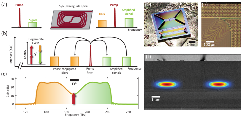
Single-pump parametric amplification can be described using a frequency-domain model of waveguide modes coupled through nonlinear degenerate four-wave mixing (DFWM) mediated by the optical Kerr effectStolen and Bjorkholm (1982); Hansryd et al. (2002), as the general principle is shown in Fig. 1(a,b). A signal and a strong pump are combined and coupled into an optical waveguide, where power is transferred from the pump to the signal via DFWM. For every annihilated pair of pump photons of frequency , a signal photon is generated together with a phase-conjugated idler photon , i.e. . In the absence of optical propagation loss, the signal power and idler power at the end of the waveguide of length follow as:
| (1) |
where and are the incident power of the signal and the pump. The parametric gain coefficient is derived as , with being the coefficient describing the effective Kerr nonlinearity. The coherent nature of parametric interaction in the waveguide demands to fulfil a stringent phase matching condition for efficient amplification:
| (2) |
where denotes the optical propagation constant, and and are the second- and fourth-order derivative with respect to . The GVD parameter of integrated waveguides can be engineered over a wide range by variation of waveguide cross-sectional geometryTurner et al. (2006); Okawachi et al. (2011). As such, both fiber- and waveguide-based TWOPA systems can provide amplification bandwidths that greatly exceed those of rare-earth-doped fiber amplifiers. Figure 1(c) depicts the maximum achievable amplification bandwidth of a 2-meter-long Si3N4 waveguide spiral with a cross-section of m2 (optimized for close to zero at the pump of 1550 nm) that can be fabricated on a mm2 size silicon chip. Such a system could exceed the EDFA’s C-band amplification bandwidth (black bar in Fig. 1(c)) by more than three times. The amplification bandwidth can be reduced by increasing the waveguide height, leading to increased anomalous GVD.
The Si3N4 photonic chip used in this work is shown in Fig. 1(d), and a microscope image of a corner of the waveguide spiral is shown in Fig. 1(e). Figure 1(f) depicts a scanning electron micrograph (SEM) of the chip cross-section, showing two Si3N4 waveguide cores of 0.91 m height and 2.45 m width. The mode profiles of the fundamental transverse-electric modes (TE00) are superimposed on the waveguide cores. We measure the spiral waveguide’s transmission spectrum, dispersion profile and propagation loss with a customized, polarization-maintaining, scanning, diode laser spectrometer and frequency-domain reflectometer (OFDR) in the wavelength range from 1260 to 1630 nm, calibrated using a self-referenced fiber-laser frequency combLiu et al. (2016). The results are presented in the Supplementary Material. The optical transmission through the 2-meter-long spiral is measured as high as 12 with a mean transmission of 10 in the wavelength range between 1545 nm and 1557 nm. The optical propagation losses are measured as low as 2.5 dB/m with a fiber-to-chip coupling loss of 2.5 dB per facet using lensed fibers and inverse tapersLiu et al. (2018a). The measured anomalous GVD is fs2mm-1, in good agreement with the result from finite-element modelling based on the measured waveguide cross-section.
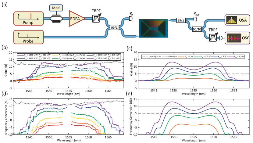
The experimental setup to measure the parametric gain and frequency conversion efficiency is depicted in Fig. 2(a). Pump and signal lasers are derived from external-cavity diode lasers. We use a high-power EDFA and a tunable bandpass filter to amplify the pump and to remove excess amplified spontaneous emission (ASE) noise. The pump and signal are combined on a fused fiber beam splitter. The signal power coupled into the photonic chip is kept below 200 W to avoid pump depletion. The signal gain and idler conversion efficiency are obtained from two signal laser wavelength scans performed in opposite direction starting at the pump wavelength and recorded on an optical spectrum analyzer (OSA) using the max-hold mode. Details are presented in the Supplementary Material. The transmission of the power-amplified pump laser is carefully optimized to 12% in agreement with the calibrated transmission measurement at low optical power. The total fiber-to-fiber loss including the fiber-chip coupling losses (two facets) and optical propagation loss in the Si3N4 waveguide spiral is marked as grey dotted lines in Fig. 2(b,d) and reaches as low as 10 dB. Therefore, we achieve for the first time a net parametric gain of up to 2 dB on a photonic chip accounting for both the on-chip optical propagation loss and the fiber-chip-fiber coupling losses. In addition, no damages of the waveguide and coupling facets are observed at input power levels up to 7 W. Notably this gain and power level are sustained without any mitigation techniques for stimulated Brillouin scattering such as fast pump laser ditheringBlows and French (2002) or phase modulationMussot et al. (2004).
As depicted in Fig. 2(b,d), the measured full bandwidths of gain and frequency conversion reach 20 nm despite the significant anomalous GVD of our thick Si3N4 waveguide. The measurement results are commensurate with our numerical calculations as shown in Fig. 2(c,e), using the full set of nonlinear equations in the frequency domainHansryd et al. (2002). Notably, the literature valueIkeda et al. (2008) widely cited for Si3N4 nonlinear refractive index of m2W-1 would result in a peak signal gain in excess of 18 dB. Recent measurementsGao and et al. (tion) of the Si3N4 nonlinear refractive index reveal a reduced value of m2W-1, likely due to a reduced fraction of Si-Si and Si-H bonds in high-temperature grown and annealed stoichiometric Si3N4 used for low absorption loss. We estimate the effective mode area as small as m2 and the effective nonlinearity of our waveguide as 0.51 W-1m-1, respectively. With these parameters, our numerical calculations predict a peak gain of 12 dB in good agreement with measurements. Fluctuations of the waveguide cross-section that flatten and broaden the parametric gain lobes, and the remaining uncertainty around the transmission loss valueKarlsson (1998), are negligible in the strong anomalous GVD regime of our waveguide.
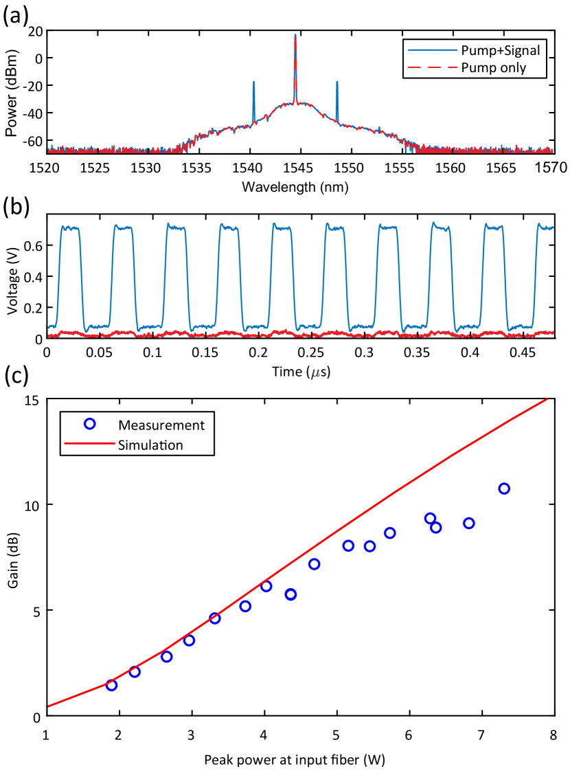
As an independent check, we also measure the parametric gain by fast modulation of the pump laser. We modulate the pump laser amplitude with a 50 MHz square wave before amplification with a duty cycle of 50%. The instantaneous nature of parametric amplification mediated by the optical Kerr effect imprints the pump modulation directly on the amplified signal and generated idler. The measurement results are depicted in Fig. 3. The pump laser is tuned to 1544.5 nm for this measurement, and the signal laser is tuned to 1548.5 nm. A second low-loss spiral is used for the measurement with similar waveguide design and from the same wafer substrate. The modulated signal beam is filtered using a tunable optical bandpass filter and is recorded on a fast photodetector. Figure 3 depicts the extracted gain values as a function of the input peak power that is seen at the tip of the lensed fiber used to couple light into the chip. The results are in agreement with numerical calculations of the gain up to a peak input power of 5 W where we see a deviation up to 2.5 dB. Still, the parametric gain is able to compensate the total losses of our photonic chip.
In summary, we present for the first time a continuous-travelling-wave optical parametric amplifier using a 2-meter-long Si3N4 nonlinear integrated waveguide that is capable to provide net gain off-chip. This advancement mirrors the breakthroughs in fiber-based rare-earth-dopedMears et al. (1987); Desurvire et al. (1987) and parametricHansryd and Andrekson (2001) amplifier technologies. The transition from fibers to nonlinear photonic integrated circuits bears great potential to improve overall device performance, footprint, and design freedom. Using advanced dispersion-engineering techniques such as vertically coupled waveguidesZhang et al. (2010) could significantly extend the parametric bandwidth by eliminating the second- and fourth-order dispersion terms in the phase mismatch. The fundamental absorption lossLiu et al. (2021) of stoichiometric Si3N4 waveguides was measured as low as 0.15 dB/m, which would facilitate parametric gain above 70 dB according to our simulations using as little as 500 mW of optical pump power, exceeding the performance of the best fiber-based parametric amplifiersTorounidis et al. (2006). Moreover, the high nonlinearity and superior Kerr-to-Brillioun gain ratioGyger et al. (2020) of Si3N4 waveguides will enable singly-resonant TWOPA with pump enhancement, which requires less footprint on chip, and greatly reduce the detrimental signal-signal FWM interaction that impeded the widespread adoption of fiber-based TWOPA originally developed in the late 1990sMarhic et al. (2015). Such integrated-photonics-based TWOPAs would be directly pumped by high-power semiconductor lasers, inherently uni-directional, high-gain, broadband, as well as time- and spectrum-continuous with a quantum-limited noise figure,. They have the potential to become long-pursued candidates for future generations of optical communication systems that operate on the full transmission bandwidth of optical fibersWinzer et al. (2018).
Methods
Fabrication process: The Si3N4 photonic chips are fabricated using an optimized photonic Damascene processPfeiffer et al. (2018a); Liu et al. (2021). The waveguide pattern are written by deep-ultraviolet (DUV) stepper lithography based on 248 nm KrF excimer laser. Advantages of using DUV stepper lithography instead of electron-beam lithography include smaller and fewer field stitching errors, easy implementation of multipass writing, and high fabrication throughput. The patterns are dry-etched to the SiO2 substrate to create waveguide preforms. The substrate is then annealed at 1250∘C (“preform reflow”)Pfeiffer et al. (2018b) to further reduce the root mean square (RMS) roughness of the waveguide sidewalls to sub-nanometer level. Stoichiometric Si3N4 film of around 1m thickness is deposited on the patterned substrate via low-pressure chemical vapor deposition (LPCVD), and fill the preform trenches to form the waveguide cores. An etchback planarization processLiu et al. (2021), combining dry etching and chemical-mechanical planarization (CMP), is used to remove excess Si3N4 and to create waveguide top surface with 0.3 nm RMS roughness. Afterwards, the substrate is annealed at 1200∘C with nitrogen atmosphere to drive out the residual hydrogen impurities in the Si3N4 filmLiu et al. (2018b); Luke et al. (2015). A top SiO2 cladding composed of TEOS and low-temperature oxide is deposited on the wafer, followed by SiO2 annealing at 1200∘C. Finally, the wafer is separated into individual photonic waveguide chips via deep dry etching followed by dicing or backside grinding.
Funding Information: This work was supported by the Air Force Office of Scientific Research (AFOSR) under Award No. FA9550-19-1-0250, by Contract HR0011-20-2-0046 (NOVEL) from the Defense Advanced Research Projects Agency (DARPA), Microsystems Technology Office (MTO), by the Swiss National Science Foundation under grant agreement No. 176563 (BRIDGE), and by the EU H2020 research and innovation programme under grant agreement No. 965124 (FEMTOCHIP). J.R. acknowledges support from the EUs H2020 research and innovation program under the Marie Sklodowska-Curie IF grant agreement no. 846737 (CoSiLiS).
Acknowledgments: We thank Tianyi Liu for helping the design, and Miles H. Anderson for the discussion. The Si3N4 chips were fabricated in the EPFL center of MicroNanoTechnology (CMi).
Author contributions: J.L. and R.N.W. designed and fabricated the samples. J.R., N.K. and J.H. performed the experiments and data analysis. J.R. performed the numerical simulations. J.R., J.L. and T.J.K. wrote the manuscript. T.J.K. supervised the project.
References
- Mears et al. (1987) R. Mears, L. Reekie, I. Jauncey, and D. Payne, in Optical Fiber Communication Conference (Optical Society of America, 1987) p. WI2.
- Desurvire et al. (1987) E. Desurvire, J. R. Simpson, and P. C. Becker, Opt. Lett. 12, 888 (1987).
- Stolen and Bjorkholm (1982) R. Stolen and J. Bjorkholm, IEEE Journal of Quantum Electronics 18, 1062 (1982).
- Hansryd et al. (2002) J. Hansryd, P. A. Andrekson, M. Westlund, J. Li, and P.-O. Hedekvist, IEEE Journal of Selected Topics in Quantum Electronics 8, 506 (2002).
- Yamamoto et al. (2008) T. Yamamoto, K. Inomata, M. Watanabe, K. Matsuba, T. Miyazaki, W. D. Oliver, Y. Nakamura, and J. Tsai, Applied Physics Letters 93, 042510 (2008).
- Clerk et al. (2010) A. A. Clerk, M. H. Devoret, S. M. Girvin, F. Marquardt, and R. J. Schoelkopf, Rev. Mod. Phys. 82, 1155 (2010).
- Macklin et al. (2015) C. Macklin, K. O’Brien, D. Hover, M. E. Schwartz, V. Bolkhovsky, X. Zhang, W. D. Oliver, and I. Siddiqi, Science 350, 307 (2015).
- Moss et al. (2013) D. J. Moss, R. Morandotti, A. L. Gaeta, and M. Lipson, Nature Photonics 7, 597 (2013).
- Gaeta et al. (2019) A. L. Gaeta, M. Lipson, and T. J. Kippenberg, Nature Photonics 13, 158 (2019).
- Foster et al. (2006) M. A. Foster, A. C. Turner, J. E. Sharping, B. S. Schmidt, M. Lipson, and A. L. Gaeta, Nature 441, 960 (2006).
- Lamont et al. (2008) M. R. Lamont, B. Luther-Davies, D.-Y. Choi, S. Madden, X. Gai, and B. J. Eggleton, Opt. Express 16, 20374 (2008).
- Kuyken et al. (2011) B. Kuyken, X. Liu, G. Roelkens, R. Baets, R. M. Osgood Jr, and W. M. Green, Optics letters 36, 4401 (2011).
- Morichetti et al. (2011) F. Morichetti, A. Canciamilla, C. Ferrari, A. Samarelli, M. Sorel, and A. Melloni, Nature communications 2, 1 (2011).
- Wang and Foster (2015) K.-Y. Wang and A. C. Foster, Journal of Optics 17, 094012 (2015).
- Pu et al. (2018) M. Pu, H. Hu, L. Ottaviano, E. Semenova, D. Vukovic, L. K. Oxenløwe, and K. Yvind, Laser & Photonics Reviews 12, 1800111 (2018).
- Ooi et al. (2017) K. Ooi, D. Ng, T. Wang, A. Chee, S. Ng, Q. Wang, L. Ang, A. Agarwal, L. Kimerling, and D. Tan, Nature communications 8, 1 (2017).
- Liu et al. (2010) X. Liu, R. M. Osgood, Y. A. Vlasov, and W. M. Green, Nature Photonics 4, 557 (2010).
- Gajda et al. (2012) A. Gajda, L. Zimmermann, M. Jazayerifar, G. Winzer, H. Tian, R. Elschner, T. Richter, C. Schubert, B. Tillack, and K. Petermann, Optics express 20, 13100 (2012).
- Liu et al. (2021) J. Liu, G. Huang, R. N. Wang, J. He, A. S. Raja, T. Liu, N. J. Engelsen, and T. J. Kippenberg, Nature Communications 12, 2236 (2021).
- Temprana et al. (2015) E. Temprana, E. Myslivets, B.-P. Kuo, L. Liu, V. Ataie, N. Alic, and S. Radic, Science 348, 1445 (2015).
- Tong et al. (2011) Z. Tong, C. Lundström, P. Andrekson, C. McKinstrie, M. Karlsson, D. Blessing, E. Tipsuwannakul, B. Puttnam, H. Toda, and L. Grüner-Nielsen, Nature photonics 5, 430 (2011).
- Marhic et al. (2015) M. E. Marhic, P. A. Andrekson, P. Petropoulos, S. Radic, C. Peucheret, and M. Jazayerifar, Laser & photonics reviews 9, 50 (2015).
- Hansryd and Andrekson (2001) J. Hansryd and P. A. Andrekson, IEEE Photonics Technology Letters 13, 194 (2001).
- Devoret and Schoelkopf (2013) M. H. Devoret and R. J. Schoelkopf, Science 339, 1169 (2013).
- Xuan et al. (2016) Y. Xuan, Y. Liu, L. T. Varghese, A. J. Metcalf, X. Xue, P.-H. Wang, K. Han, J. A. Jaramillo-Villegas, A. A. Noman, C. Wang, S. Kim, M. Teng, Y. J. Lee, B. Niu, L. Fan, J. Wang, D. E. Leaird, A. M. Weiner, and M. Qi, Optica 3, 1171 (2016).
- Ji et al. (2017) X. Ji, F. A. S. Barbosa, S. P. Roberts, A. Dutt, J. Cardenas, Y. Okawachi, A. Bryant, A. L. Gaeta, and M. Lipson, Optica 4, 619 (2017).
- Ye et al. (2019) Z. Ye, K. Twayana, P. A. Andrekson, and V. Torres-Company, Opt. Express 27, 35719 (2019).
- Pu et al. (2016) M. Pu, L. Ottaviano, E. Semenova, and K. Yvind, Optica 3, 823 (2016).
- Chang et al. (2020) L. Chang, W. Xie, H. Shu, Q.-F. Yang, B. Shen, A. Boes, J. D. Peters, W. Jin, C. Xiang, S. Liu, G. Moille, S.-P. Yu, X. Wang, K. Srinivasan, S. B. Papp, K. Vahala, and J. E. Bowers, Nature Communications 11, 1331 (2020).
- Wilson et al. (2020) D. J. Wilson, K. Schneider, S. Hönl, M. Anderson, Y. Baumgartner, L. Czornomaz, T. J. Kippenberg, and P. Seidler, Nature Photonics 14, 57 (2020).
- Belt et al. (2017) M. Belt, M. L. Davenport, J. E. Bowers, and D. J. Blumenthal, Optica 4, 532 (2017).
- Jung et al. (2021) H. Jung, S.-P. Yu, D. R. Carlson, T. E. Drake, T. C. Briles, and S. B. Papp, Optica 8, 811 (2021).
- Eggleton et al. (2011) B. J. Eggleton, B. Luther-Davies, and K. Richardson, Nature Photonics 5, 141 (2011).
- Liu et al. (2019) Y. Liu, A. Choudhary, G. Ren, K. Vu, B. Morrison, A. Casas-Bedoya, T. G. Nguyen, D.-Y. Choi, P. Ma, A. Mitchell, S. J. Madden, D. Marpaung, and B. J. Eggleton, APL Photonics, APL Photonics 4, 106103 (2019).
- Kim et al. (2020) D.-G. Kim, S. Han, J. Hwang, I. H. Do, D. Jeong, J.-H. Lim, Y.-H. Lee, M. Choi, Y.-H. Lee, D.-Y. Choi, and H. Lee, Nature Communications 11, 5933 (2020).
- Pfeiffer et al. (2018a) M. H. P. Pfeiffer, C. Herkommer, J. Liu, T. Morais, M. Zervas, M. Geiselmann, and T. J. Kippenberg, IEEE Journal of Selected Topics in Quantum Electronics 24, 1 (2018a).
- Levy et al. (2010) J. S. Levy, A. Gondarenko, M. A. Foster, A. C. Turner-Foster, A. L. Gaeta, and M. Lipson, Nature Photonics 4, 37 (2010).
- Gyger et al. (2020) F. Gyger, J. Liu, F. Yang, J. He, A. S. Raja, R. N. Wang, S. A. Bhave, T. J. Kippenberg, and L. Thévenaz, Phys. Rev. Lett. 124, 013902 (2020).
- Okawachi et al. (2011) Y. Okawachi, K. Saha, J. S. Levy, Y. H. Wen, M. Lipson, and A. L. Gaeta, Opt. Lett. 36, 3398 (2011).
- Turner et al. (2006) A. C. Turner, C. Manolatou, B. S. Schmidt, M. Lipson, M. A. Foster, J. E. Sharping, and A. L. Gaeta, Optics express 14, 4357 (2006).
- Liu et al. (2016) J. Liu, V. Brasch, M. H. P. Pfeiffer, A. Kordts, A. N. Kamel, H. Guo, M. Geiselmann, and T. J. Kippenberg, Opt. Lett. 41, 3134 (2016).
- Liu et al. (2018a) J. Liu, A. S. Raja, M. H. P. Pfeiffer, C. Herkommer, H. Guo, M. Zervas, M. Geiselmann, and T. J. Kippenberg, Opt. Lett. 43, 3200 (2018a).
- Blows and French (2002) J. L. Blows and S. E. French, Optics letters 27, 491 (2002).
- Mussot et al. (2004) A. Mussot, A. Durecu-Legrand, E. Lantz, C. Simonneau, D. Bayart, H. Maillotte, and T. Sylvestre, IEEE Photonics Technology Letters 16, 1289 (2004).
- Ikeda et al. (2008) K. Ikeda, R. E. Saperstein, N. Alic, and Y. Fainman, Optics express 16, 12987 (2008).
- Gao and et al. (tion) M. Gao and et al., (manuscript in preparation).
- Karlsson (1998) M. Karlsson, JOSA B 15, 2269 (1998).
- Zhang et al. (2010) L. Zhang, Y. Yue, R. G. Beausoleil, and A. E. Willner, Optics express 18, 20529 (2010).
- Torounidis et al. (2006) T. Torounidis, P. A. Andrekson, and B.-E. Olsson, IEEE Photonics Technology Letters 18, 1194 (2006).
- Winzer et al. (2018) P. J. Winzer, D. T. Neilson, and A. R. Chraplyvy, Opt. Express 26, 24190 (2018).
- Pfeiffer et al. (2018b) M. H. P. Pfeiffer, J. Liu, A. S. Raja, T. Morais, B. Ghadiani, and T. J. Kippenberg, Optica 5, 884 (2018b).
- Liu et al. (2018b) J. Liu, A. S. Raja, M. Karpov, B. Ghadiani, M. H. P. Pfeiffer, B. Du, N. J. Engelsen, H. Guo, M. Zervas, and T. J. Kippenberg, Optica 5, 1347 (2018b).
- Luke et al. (2015) K. Luke, Y. Okawachi, M. R. E. Lamont, A. L. Gaeta, and M. Lipson, Opt. Lett. 40, 4823 (2015).