Impact of the absorber coupling design for Transition Edge Sensor X-ray Calorimeters
Abstract
Transition Edge Sensors (TESs) are the selected technology for future spaceborne X-ray observatories, such as Athena, Lynx, and HUBS. These missions demand thousands of pixels to be operated simultaneously with high energy-resolving power. To reach these demanding requirements, every aspect of the TES design has to be optimized. Here we present the experimental results of tests on different devices where the coupling between the x-ray absorber and the TES sensor is varied. In particular, we look at the effects of the diameter of the coupling stems and the distance between the stems and the TES bilayer. Based on measurements of the AC complex impedance and noise, we observe a reduction in the excess noise as the spacing between the absorber stem and the bilayer is decreased. We identify the origin of this excess noise to be internal thermal fluctuation noise between the absorber stem and the bilayer. Additionally, we see an impact of the coupling on the superconducting transition in the appearance of kinks. Our observations show that these unwanted structures in the transition shape can be avoided with careful design of the coupling geometry. Also the stem diameter appears to have a significant impact on the smoothness of the TES transition. This observation is still poorly understood, but is of great importance for both AC and DC biased TESs.
I Introduction
Transition Edge Sensors (TESs) are very sensitive detectors of energy that utilize the sharpness of a superconductor normal-to-superconducting transitionIrwin and Hilton (2005); Ullom and Bennett (2015); Gottardi and Nagayashi (2021). TESs are the selected technology in a number of either planned or proposed space-borne observatories, such as Athena Barret et al. (2020), Lynx Gaskin and Swartz (2019), and HUBS Cui et al. (2020). These missions aim for thousands of pixels to be operated simultaneously with high energy resolving power. The limited resources available for a satellite-based instrument, such as electrical power, cooling power, and allowable weight, require the use of sophisticated multiplexing schemes, such as Time Division Multiplexing (TDM) Durkin et al. (2019), Frequency Division Multiplexing (FDM) Akamatsu et al. (2020), and others Morgan et al. (2016); Bennett et al. (2019); Nakashima et al. (2020). In this paper, we focus on TES based X-ray micro-calorimeters developed for the Athena X-ray Integral Field Unit (X-IFU) instrument Pajot et al. (2018). X-IFU will consist of over 3000 multiplexed pixels with a planned spectral resolution of 2.5 eV for 7 keV X-rays.
In order to achieve the demanding requirements set by the X-IFU instrument, every aspect of the TES pixel design has to be optimized. Over the years much work has been done towards this goal. Research topics included the impact of the thermal conductance on the TES transition width Hays-Wehle et al. (2016); Morgan et al. (2017); Zhang et al. (2019), the impact of the normal resistance by changing the TES size and aspect ratio Gottardi et al. (2017); Sakai et al. (2018); Morgan et al. (2019); De Wit et al. (2020), the noise-mitigating properties of normal-metal features Ullom et al. (2004); Sadleir et al. (2011); Miniussi et al. (2018); Wakeham et al. (2018), and how the energy deposited in the absorbed is transferred to the bilayer Kilbourne et al. (2007); Smith et al. (2012, 2014). In this paper, we expand on this last point by studying how the detailed design of the coupling between the X-ray absorber and the TES bilayer affects the properties of the TES micro-calorimeters. The basic layout of the TESs are explained in Sec. II of this paper.
Previous work has shown that the design of the coupling geometry could have a big impact on the detector properties. It was demonstrated that the stems introduce effects of non-equilibrium superconductivity via the proximity effect, affecting the critical temperature and critical current, and influence the small-signal transition parameters and , and the detector energy resolution and time constants Bandler et al. (2008); Sadleir et al. (2011); Smith et al. (2013, 2014). Note that these effects were reported for stems with a very large footprint on the bilayer, while in this work, we study the impact of much smaller stems, which will allow us to pick up on more subtle differences than those reported before. We mainly investigate the effect of the diameter of the two stems that connects the absorber to the bilayer, and the spacing between these two. We measured the complex impedance and noise, which are used to estimate the internal thermal conductance in the TES and how this is influenced by the geometry. We compare the small-signal limit energy resolution, estimated from the measured noise and transition shape, with the measured Noise Equivalent Power (NEP), and find a good qualitative agreement between the two.
II Detectors and Measurement Setup
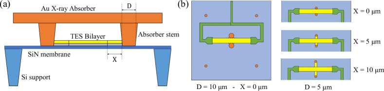
We have fabricated an TES array with four different geometries for the absorber-bilayer coupling. The basic layout of the detectors is shown schematically in Fig. 1(a). The TESs are based on a bilayer made of 35 nm Ti and 200 nm Au, with a sheet resistance of 26 m/. The bilayer is patterned to be an m2 rectangle with a normal resistance of approximately 200 m. Niobium leads are used to apply a voltage bias to the devices. The bilayers are grown on a 0.5m thick silicon nitride membrane. The TES is connected to an Au X-ray absorber via two central absorber stems with a height of 3.5 m, one at each edge of the bilayer. Four additional stems (not shown in Fig. 1(a)) with diameter 5 m are used to support the absorber on the membrane. The absorber has a thickness of 2.35 m and a heat capacity of 0.85 pJ/K at 90 mK. Further details about the TESs and the fabrication procedure are given by Nagayoshi et al.Nagayoshi et al. (2019).
To study how the detailed coupling between the absorber and the bilayer affects the detector properties, we vary the geometry of the two absorber stems, as schematically illustrated in Fig. 1(b). We look at the possible impact of the diameter of the two central stems, by comparing two designs with diameters m and m, both fabricated such that the edge of the bilayer is aligned with the edge of the outer perimeter of the stem. Additionally, we look at whether the precise position of the stems is of importance for the final detector performance, by comparing three designs with the same diameter m but different spacing between the edge of the bilayer and the edge of the stems, , , and m. The arm connecting the stem and the bilayer is an integral part of the bilayer, deposited in the same step of the fabrication. All other properties of the devices are identical to allow for direct comparison.
We characterize the devices using an FDM setup, with which we bias a single pixel at a time within the superconducting transition using an alternating current (AC). The resistance of the TES at a particular bias point is generally specified with respect to the normal resistance . Each of the investigated pixels is connected to a high-Q LC resonator Bruijn et al. (2012) with a bias frequency between 1-5 MHz. Further details about the FDM setup are given elsewhere Akamatsu et al. (2016); De Wit et al. (2020). Most of the results presented in the remainder of this paper do not depend on the bias frequency, and are valid for both AC and DC biased pixels. Therefore, we focus on presenting results from pixels measured at low bias frequencies (MHz), as these results are typically more straightforward to interpret and compare to the literature.
The setup is mounted at the mixing-chamber of a cryogen-free dilution refrigerator, and is stabilized at a temperature of 50 mK. External magnetic fields are shielded using a room-temperature -metal shield and a lead and cryoperm shield at the cold stage. Both the setup and the cryoperm shield are suspended from a kevlar vibration isolation stage for mechanical decoupling Gottardi et al. (2019). A more extensive overview of the setup is given elsewhere De Wit et al. (2020).
For all devices measurements of the current-voltage characteristic (IV-curve) at different bath temperatures are used to determine the critical temperature and thermal conductance of the detectors. The averaged thermal conductance for all devices is 46.5 pW/K with a standard deviation of 4.6 pW/K at a critical temperature of mK. Given the fact that the thermal conductance of this type of devices is generally proportional to the phonon-emitting perimeter of the TES Hoevers et al. (2005); Hays-Wehle et al. (2016); De Wit et al. (2020), the thermal conductance is expected to increase for larger , with a difference of approximately 7 pW/K between the and m devices. This predicted difference has not been resolved in the measured data. We have observed no effect of the stem geometry on the current distribution, nor in the temperature dependence of the critical current.
III Impact of Stem-Bilayer Distance
We fully characterize the properties of the transition by measuring the complex impedance of the TES Lindeman et al. (2004). For various points in the transition, a small modulation is added to the bias current with a frequency ranging from HzkHz, where we record the TES response for each frequency. This data is combined with knowledge of the heat capacity, which is dominated by the X-ray absorber, and thermal conductance to extract the dimensionless derivatives of the resistance with respect to the temperature and to the current . We focus on these parameters, as they describe the shape of the superconducting transition and can be used to obtain, among other things, the bandwidth and sensitivity of the detectors. Details of this measurement and analysis under AC bias are given elsewhere Taralli et al. (2019); Gottardi et al. (2021). Representative data for and for low bias frequency devices with varying length of the arm between the absorber and the bilayer is shown in Fig. 2.
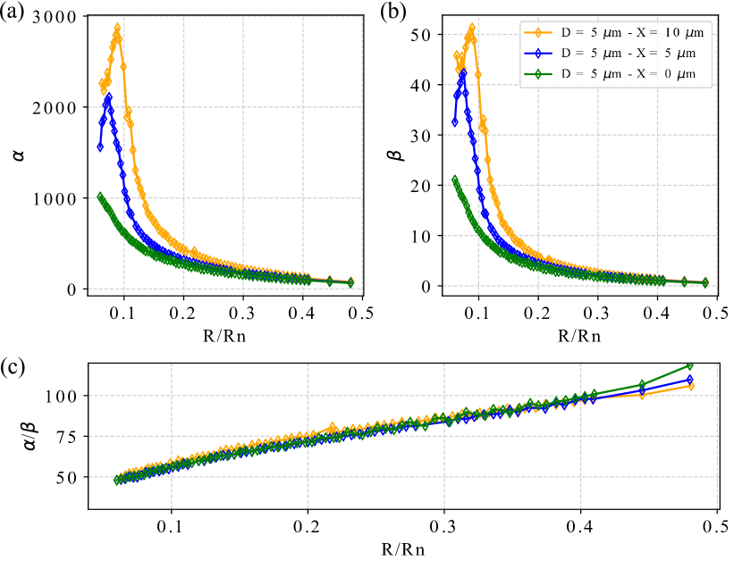
All the devices show a similar ratio between , visible in Fig. 2(c). However, there are clear differences between the devices low in the resistive transition, as visible in Figs. 2(a) and (b). The m and m devices show high peaks in both and , signs of sharp features or kinks in the superconducting transition. No kinks are observed for the m devices for all measured bias frequencies. Kinks are regularly observed in devices with normal metal stripes on top of the TES Smith et al. (2015); Wakeham et al. (2018). Here we show that also the normal metal of the absorber stems might play a role in the precise location of these kinks in the transition. For the shortest arms with m, the kinks are absent or might have shifted to lower resistance values outside of the region of interest. The removal of kinks from the relevant region of the parameter space is of utmost importance for achieving uniform performance in large arrays of TESs.
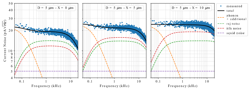
Apart from the complex impedance, for each bias point we have measured the current noise spectrum. Example noise spectra for the three m pixels measured at are shown by the blue points in Fig. 3. The roll-off visible at high frequencies results from the bandwidth of the electrical circuit.
We can compare the measured noise spectra with the calculated contributions from various noise sources. The principal sources of noise include the white readout noise of the SQUID, low frequency phonon noise coming from thermal fluctuations between the TES and the bath (and other low frequency noise sources such as vibrations and stray photons, all summed under the name additional low frequency noise), and Johnson noise from the TES resistance. It has recently been shown that for this type of devices the Johnson noise is best described by the Resistively-Shunted-Junction (RSJ) model Kozorezov et al. (2012); Gottardi et al. (2021); Wessels et al. (2021), given by:
| (1) |
with being the Boltzmann constant. These main sources of noise are shown as the various dashed lines in Fig. 3. However, the sum of these noise sources is clearly insufficient to fully explained the measured noise. Therefore, we express the factor of difference between the measured noise and the predicted noise using the parameter , defined by:
| (2) |
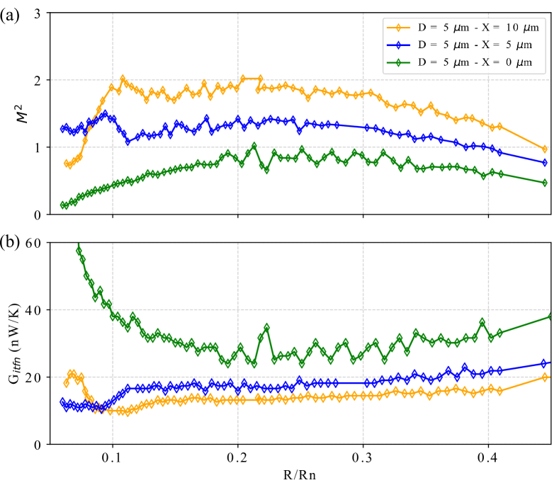
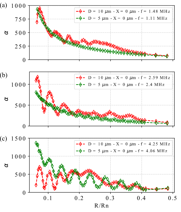
Fig. 4(a) shows for various bias points in the transition for the different designs, showing a clear rise in as increases.
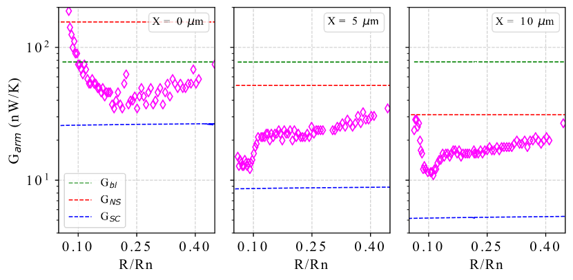
In order to explain the additional noise in the kHz range, we interpret it as resulting from internal thermal fluctuation noise (ITFN) within the detector itself Wakeham et al. (2019); Gottardi et al. (2021). ITFN occurs when there are distributed heat capacities inside the detector connected by internal thermal impedances. Such a complex thermal structure results in thermal fluctuations between the different heat capacities. To confirm this hypothesis we add another noise contribution coming from the ITFN, given by , where is a thermal conductance located within the TES Palosaari et al. (2012); Maasilta (2012). This contribution is shown as the red dashed lines in Fig. 3. Note that the shape of the ITFN is similar to the RSJ Johnson noise due to the conversion of power to current noise via the power-to-current responsivity and the TES circuit inductance. is treated as a free parameter to be varied such that is minimized. The resulting is shown in Fig. 4(b). As expected, the internal thermal conductance decreases as increases. At %, the extracted increases from nW/K for m to nW/K for m and finally to nW/K for m.
The internal thermal conductance is believed to be a combination of the internal thermal conductance of the bilayer , and the limited thermal conductance of the arm between the absorber stem and the bilayer, . Using the simplest possible thermal model in which the different thermal components are connected in parallel, can be estimated from the measured using:
| (3) |
The internal thermal conductance of the bilayer is estimated by using the Wiedemann-Franz law, , with and the sheet resistance of the bilayer Gottardi et al. (2021). For the m2 devices, nW/K. The estimated is shown as the magenta points in Fig. 5.
To understand the origin of the limited thermal conductance of the arm, we estimate it in two limiting regimes. The upper limit is given by the normal state thermal conductance of the arm , which again is estimated using the Wiedemann-Franz law. In this case the resistance of the arm is calculated using an effective length , the full length of the arm including the end part covered by the absorber stem. This upper limit is shown in Fig. 5 as the red dashed lines. The lower limit is obtained by assuming that the arm remains superconducting. As cooper pairs cannot transport heat the thermal conductance is purely governed by the fraction of depaired electrons, which is dictated by the temperature dependent superconducting gap and the thermal excitation energy . Thus, the thermal conductance can be estimated using:
| (4) |
In order to evaluate this equation knowledge about the temperature dependence of the superconducting gap is required. For a conventional s-wave superconductor at , this dependence is given by
| (5) |
with the gap at T = 0 Tinkham (1996). However, this is not valid in the presence of the proximity effect, which significantly alters the size of the gap close to the of the bilayer. Therefore, we simplify the problem and derive a lower limit for the thermal conductance by neglecting the temperature dependence of the gap and using . The resulting is shown as the blue dashed lines in Fig. 5. Indeed the values for extracted from the experimental data fall between these two boundaries, supporting the interpretation that the arm partially remains superconducting with a that is suppressed compared to the ideal value, but remains finite.
The previous analysis clearly indicates that a small but significant reduction of the excess noise can be achieved by keeping the stem as close to the bilayer as possible, or perhaps by even placing the stems on top of the bilayerWakeham et al. (2020). Note that after reducing the ITFN, the performance of this type of devices under these conditions will remain limited by the noise resulting from the weak-link effect as described by the RSJ model.
IV Impact of Stem-Bilayer Diameter
The main effects of the stem diameter are visible in the measured , shown in Fig. 6, and excess noise, shown in Fig. 7. In these figures, we focus on the designs with m. Three different sets of pixels are selected, measured at (a) low, (b) mid, and (c) high bias frequencies, the precise values of which are indicated in the legend of Fig. 6.
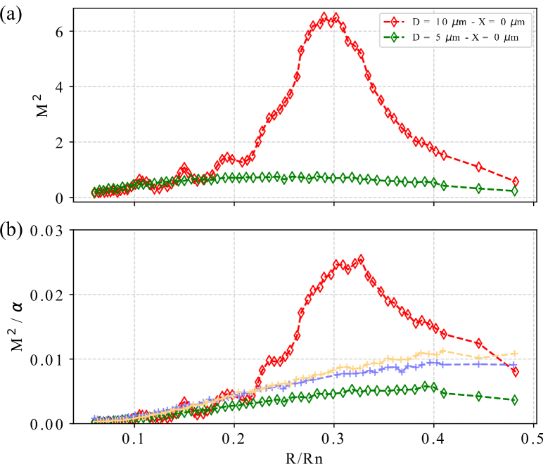
Changing the stem diameter from to m does not change the overall trend of . However, there is a striking difference between how , and consequently and , changes throughout the transition. The m devices show large oscillations of for different bias points. These oscillations are typically attributed to the weak-link effect in these detectors Gottardi et al. (2018); De Wit et al. (2020) resulting from the interaction between the high Nb leads and the low bilayer. However, the amplitude of the oscillations is much smaller for all m devices, except for those measured at the highest bias frequencies as visible in Fig. 6(c). In order to confirm this observation and to understand the underlying mechanism for why the smaller stem diameter improves the smoothness of the superconducting transition, more devices with different stem diameters should be studied.
Another interesting feature of the smaller stem diameter is visible in the excess noise in Fig. 7(a). For all the devices studied in this work with m, a peak in the excess noise is visible between . This peak is never observed for any of the devices with m. These devices do show a bump in the transition around , visible in Fig. 2, but in those cases the increase in alpha is correlated with an increase in . This is not the case for the m devices, a fact that becomes clear when looking at Fig. 7(b), in which we plot . The stark difference in the ratio of and between the m data (red points) and the other data signifies the difference in nature of the bump in the excess noise.
The exact origin for the excess noise bumps is unclear, but we believe that it’s related to a scattering or interference effect of the quasi-particles interacting with the normal metal stems. A new set of devices is currently under fabrication to study these effects in more detail.
V NEP and energy resolution
Arguably the most important figure of merit for a micro-calorimeter is the energy resolution, i.e. the capacity to resolve different photon energies. In this section, we demonstrate the effect of the absorber coupling geometry in two ways. First, we evaluate the integrated noise-equivalent power (NEP) at 5.9 keV for bias points between . The NEP is generally a good predictor for the achievable energy resolution in the large-signal limit. Secondly, we can use , , and , as shown in Secs. III and IV, to calculate the expected energy resolution in the small-signal limit for each bias point, using:
| (6) |
The results for the NEP and expected energy resolution are shown in Fig. 8 for four different pixels, one of each design, measured at low bias frequencies. In absolute terms, a relatively large difference is observed between the NEP and estimated . This is most likely the result from the fact that our detectors are working outside of the small-signal limit for 5.9 keV X-rays. Note that the increase in NEP and seen in the m device at higher is caused by the bump in the excess noise shown in Fig. 7.
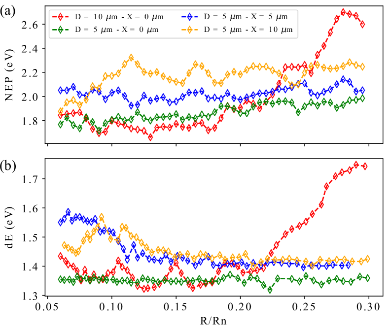
The NEP and qualitatively give the same results, and confirm the trends previously identified. The best energy resolutions are expected for the devices with m. As the length of the arm between the absorber and the bilayer increases, the energy resolution becomes worse. This observation holds over the full bias frequency range. The increase in the energy resolution is about eV, and clearly indicates that maximizing the thermal conductance between the absorber and the bilayer is of great importance to optimize the resolution. The effect of the stem diameter is much less pronounced, with only a very small reduction of less than 0.1 eV for both the NEP and . This is not completely unexpected. If we assume that the gold in the absorber stem has a electrical resistivity nm, similar to previously reported values Wakeham et al. (2019), the Wiedemann-Franz law can be used to estimate a thermal conductance of the stem (with height 3.5 m). This leads to W/K and W/K for the m and m diameter stems, respectively. For both diameters, is much higher that the estimated thermal conductance of the arm, and therefore does not play a significant role in the noise.
VI Conclusions
We have studied the impact of the detailed geometry for the thermal coupling between the X-ray absorber and the bilayer, with a particular focus on the diameter of the two stems that connect the absorber to the TES bilayer, and the spacing between the stems and the bilayer.
Based on measurements of the noise, we found that the noise is reduced for shorter arms, an observation that we explain in terms of a higher internal thermal conductance between the absorber and the TES. Additionally, we observe that the position of kinks in the superconducting transition is affected by the spacing between the stems. While a more thorough investigation is required to fully understand the responsible mechanism, the effect appears to be related to previously reported observations in devices with added normal-metal structures on top of the bilayer. Comparing the devices with different stem diameters resulted in the striking observation that the smoothness of the transition seems to be significantly improved for the smaller stem diameter. Testing of additional devices of different geometry should help to confirm this observation. These devices are currently under fabrication.
The conclusion of this study is that the stems should be placed as close to the bilayer as possible in order to reduce the internal thermal fluctuation noise, leading to an improved energy resolution of up to 0.4 eV. This observation is consistent with the results from similar studies Wakeham et al. (2020). The optimization of the stem diameter is more complicated. For the energy resolution, increasing the diameter could further reduce the ITFN and give better energy resolutions in certain bias points (even though the effect will be quite modest). However, our results suggest that reducing the stem diameter, or perhaps only using a single supporting stem, might greatly improve the smoothness and uniformity of the normal-to-superconducting transition, a feature that is of great importance for the successful operation of large number of TESs in any multiplexing scheme.
VII Acknowledgement
SRON is supported financially by NWO, the Netherlands Organization for Scientific Research. This work is partly funded by European Space Agency (ESA) and coordinated with other European efforts under ESA CTP contract ITT AO/1-7947/14/NL/BW.
VIII Data Availability
The data that support the findings of this study are available from the corresponding author upon reasonable request.
References
- Irwin and Hilton (2005) K. Irwin and G. Hilton, Transition-Edge Sensors, in Topics Appl. Phys., Vol. 99 (2005) pp. 63–150.
- Ullom and Bennett (2015) J. N. Ullom and D. A. Bennett, Review of superconducting transition-edge sensors for x-ray and gamma-ray spectroscopy, Superconductor Science and Technology 28, 084003 (2015).
- Gottardi and Nagayashi (2021) L. Gottardi and K. Nagayashi, A review of X-ray microcalorimeters based on superconducting transition edge sensors for astrophysics and particle physics, Applied Sciences (Switzerland) 11, 10.3390/app11093793 (2021).
- Barret et al. (2020) D. Barret, A. Decourchelle, A. Fabian, M. Guainazzi, K. Nandra, R. Smith, and J.-W. den Herder, The Athena space X-ray observatory and the astrophysics of hot plasma†, Astronomische Nachrichten 341, 224 (2020), arXiv:1912.04615 .
- Gaskin and Swartz (2019) J. A. Gaskin and D. A. Swartz, Lynx X-Ray Observatory: an overview, Journal of Astronomical Telescopes, Instruments, and Systems 5, 1 (2019).
- Cui et al. (2020) W. Cui, L. B. Chen, B. Gao, F. L. Guo, H. Jin, G. L. Wang, L. Wang, J. J. Wang, W. Wang, Z. S. Wang, Z. Wang, F. Yuan, and W. Zhang, HUBS: Hot Universe Baryon Surveyor, Journal of Low Temperature Physics 199, 502 (2020).
- Durkin et al. (2019) M. Durkin, J. S. Adams, S. R. Bandler, J. A. Chervenak, S. Chaudhuri, C. S. Dawson, E. V. Denison, W. B. Doriese, S. M. Duff, F. M. Finkbeiner, C. T. Fitzgerald, J. W. Fowler, J. D. Gard, G. C. Hilton, K. D. Irwin, Y. I. Joe, R. L. Kelley, C. A. Kilbourne, A. R. Miniussi, K. M. Morgan, G. C. O’Neil, C. G. Pappas, F. S. Porter, C. D. Reintsema, D. A. Rudman, K. Sakai, S. J. Smith, R. W. Stevens, D. S. Swetz, P. Szypryt, J. N. Ullom, L. R. Vale, N. A. Wakeham, J. C. Weber, and B. A. Young, Demonstration of athena X-IFU compatible 40-row time-division-multiplexed readout, IEEE Transactions on Applied Superconductivity 29, 1 (2019).
- Akamatsu et al. (2020) H. Akamatsu, L. Gottardi, J. van der Kuur, C. P. de Vries, M. P. Bruijn, J. A. Chervenak, M. Kiviranta, A. J. van den Linden, B. D. Jackson, A. R. Miniussi, K. Ravensberg, K. Sakai, S. J. Smith, and N. Wakeham, Progress in the Development of Frequency-Domain Multiplexing for the X-ray Integral Field Unit on Board the Athena Mission, Journal of Low Temperature Physics 199, 737 (2020).
- Morgan et al. (2016) K. M. Morgan, B. K. Alpert, D. A. Bennett, E. V. Denison, W. B. Doriese, J. W. Fowler, J. D. Gard, G. C. Hilton, K. D. Irwin, Y. I. Joe, G. C. O’Neil, C. D. Reintsema, D. R. Schmidt, J. N. Ullom, and D. S. Swetz, Code-division-multiplexed readout of large arrays of TES microcalorimeters, Applied Physics Letters 109, 112604 (2016).
- Bennett et al. (2019) D. A. Bennett, J. A. B. Mates, S. R. Bandler, D. T. Becker, J. W. Fowler, J. D. Gard, G. C. Hilton, K. D. Irwin, K. M. Morgan, C. D. Reintsema, K. Sakai, D. R. Schmidt, S. J. Smith, D. S. Swetz, J. N. Ullom, L. R. Vale, and A. L. Wessels, Microwave SQUID multiplexing for the Lynx x-ray microcalorimeter, Journal of Astronomical Telescopes, Instruments, and Systems 5, 1 (2019).
- Nakashima et al. (2020) Y. Nakashima, F. Hirayama, S. Kohjiro, H. Yamamori, S. Nagasawa, A. Sato, S. Yamada, R. Hayakawa, N. Y. Yamasaki, K. Mitsuda, K. Nagayoshi, H. Akamatsu, L. Gottardi, E. Taralli, M. P. Bruijn, M. L. Ridder, J. R. Gao, and J. W. Den Herder, Low-noise microwave SQUID multiplexed readout of 38 x-ray transition-edge sensor microcalorimeters, Applied Physics Letters 117, 3 (2020).
- Pajot et al. (2018) F. Pajot, D. Barret, T. Lam-Trong, J.-W. den Herder, L. Piro, M. Cappi, J. Huovelin, R. Kelley, J. M. Mas-Hesse, K. Mitsuda, S. Paltani, G. Rauw, A. Rozanska, J. Wilms, M. Barbera, F. Douchin, H. Geoffray, R. H. den Hartog, C. Kilbourne, M. Le Du, C. Macculi, J. M. Mesnager, and P. Peille, The Athena X-ray Integral Field Unit (X-IFU), Journal of Low Temperature Physics 193, 901 (2018).
- Hays-Wehle et al. (2016) J. P. Hays-Wehle, D. R. Schmidt, J. N. Ullom, and D. S. Swetz, Thermal Conductance Engineering for High-Speed TES Microcalorimeters, Journal of Low Temperature Physics 184, 492 (2016).
- Morgan et al. (2017) K. M. Morgan, C. G. Pappas, D. A. Bennett, J. D. Gard, J. P. Hays-Wehle, G. C. Hilton, C. D. Reintsema, D. R. Schmidt, J. N. Ullom, and D. S. Swetz, Dependence of transition width on current and critical current in transition-edge sensors, Applied Physics Letters 110, 2 (2017).
- Zhang et al. (2019) X. Zhang, S. M. Duff, G. C. Hilton, P. J. Lowell, K. M. Morgan, D. R. Schmidt, and J. N. Ullom, Controlling the thermal conductance of silicon nitride membranes at 100 mK temperatures with patterned metal features, Applied Physics Letters 115, 052601 (2019).
- Gottardi et al. (2017) L. Gottardi, H. Akamatsu, J. van der Kuur, S. J. Smith, A. Kozorezov, and J. Chervenak, Study of TES-Based Microcalorimeters of Different Size and Geometry Under AC Bias, IEEE Transactions on Applied Superconductivity 27, 1 (2017).
- Sakai et al. (2018) K. Sakai, J. S. Adams, S. R. Bandler, J. A. Chervenak, A. M. Datesman, M. E. Eckart, F. M. Finkbeiner, R. L. Kelley, C. A. Kilbourne, A. R. Miniussi, F. S. Porter, J. S. Sadleir, S. J. Smith, N. A. Wakeham, E. J. Wassell, W. Yoon, H. Akamatsu, M. P. Bruijn, L. Gottardi, B. D. Jackson, J. van der Kuur, B. J. van Leeuwen, A. J. van der Linden, H. J. van Weers, and M. Kiviranta, Study of Dissipative Losses in AC-Biased Mo/Au Bilayer Transition-Edge Sensors, Journal of Low Temperature Physics 193, 356 (2018).
- Morgan et al. (2019) K. M. Morgan, D. T. Becker, D. A. Bennett, W. B. Doriese, J. D. Gard, K. D. Irwin, S. J. Lee, D. Li, J. A. Mates, C. G. Pappas, D. R. Schmidt, C. J. Titus, D. D. Van Winkle, J. N. Ullom, A. Wessels, and D. S. Swetz, Use of Transition Models to Design High Performance TESs for the LCLS-II Soft X-Ray Spectrometer, IEEE Transactions on Applied Superconductivity 29, 1 (2019).
- De Wit et al. (2020) M. De Wit, L. Gottardi, E. Taralli, K. Nagayoshi, M. L. Ridder, H. Akamatsu, M. P. Bruijn, M. D’Andrea, J. Van Der Kuur, K. Ravensberg, D. Vaccaro, S. Visser, J. R. Gao, and J. W. Den Herder, High aspect ratio transition edge sensors for x-ray spectrometry, Journal of Applied Physics 128, 10.1063/5.0029669 (2020).
- Ullom et al. (2004) J. N. Ullom, W. B. Doriese, G. C. Hilton, J. A. Beall, S. Deiker, W. D. Duncan, L. Ferreira, K. D. Irwin, C. D. Reintsema, and L. R. Vale, Characterization and reduction of unexplained noise in superconducting transition-edge sensors, Applied Physics Letters 84, 4206 (2004).
- Sadleir et al. (2011) J. E. Sadleir, S. J. Smith, I. K. Robinson, F. M. Finkbeiner, J. A. Chervenak, S. R. Bandler, M. E. Eckart, and C. A. Kilbourne, Proximity effects and nonequilibrium superconductivity in transition-edge sensors, Physical Review B 84, 184502 (2011).
- Miniussi et al. (2018) A. R. Miniussi, J. S. Adams, S. R. Bandler, J. A. Chervenak, A. M. Datesman, M. E. Eckart, A. J. Ewin, F. M. Finkbeiner, R. L. Kelley, C. A. Kilbourne, F. S. Porter, J. E. Sadleir, K. Sakai, S. J. Smith, N. A. Wakeham, E. J. Wassell, and W. Yoon, Performance of an X-ray Microcalorimeter with a 240 m Absorber and a 50 m TES Bilayer, Journal of Low Temperature Physics 193, 337 (2018).
- Wakeham et al. (2018) N. A. Wakeham, J. S. Adams, S. R. Bandler, J. A. Chervenak, A. M. Datesman, M. E. Eckart, F. M. Finkbeiner, R. L. Kelley, C. A. Kilbourne, A. R. Miniussi, F. S. Porter, J. E. Sadleir, K. Sakai, S. J. Smith, E. J. Wassell, and W. Yoon, Effects of Normal Metal Features on Superconducting Transition-Edge Sensors, Journal of Low Temperature Physics 193, 231 (2018).
- Kilbourne et al. (2007) C. A. Kilbourne, S. R. Bandler, A. D. Brown, J. A. Chervenak, E. Figueroa-Feliciano, F. M. Finkbeiner, N. Iyomoto, R. L. Kelley, F. S. Porter, and S. J. Smith, Uniform high spectral resolution demonstrated in arrays of TES x-ray microcalorimeters, UV, X-Ray, and Gamma-Ray Space Instrumentation for Astronomy XV 6686, 668606 (2007).
- Smith et al. (2012) S. J. Smith, J. S. Adams, M. E. Eckart, C. N. Bailey, S. R. Bandler, J. A. Chervenak, F. M. Finkbeiner, R. L. Kelley, C. A. Kilbourne, F. S. Porter, and J. E. Sadleir, Small pitch transition-edge sensors with broadband high spectral resolution for solar physics, Journal of Low Temperature Physics 167, 168 (2012).
- Smith et al. (2014) S. J. Smith, J. S. Adams, S. R. Bandler, S. E. Busch, J. A. Chervenak, M. E. Eckart, F. M. Finkbeiner, R. L. Kelley, C. A. Kilbourne, S. J. Lee, J. P. Porst, F. S. Porter, and J. E. Sadleir, Characterization of Mo/Au transition-edge sensors with different geometric configurations, Journal of Low Temperature Physics 176, 356 (2014).
- Bandler et al. (2008) S. R. Bandler, R. P. Brekosky, A. D. Brown, J. A. Chervenak, E. Figueroa-Feliciano, F. M. Finkbeiner, N. Iyomoto, R. L. Kelley, C. A. Kilbourne, F. S. Porter, J. Sadleir, and S. J. Smith, Performance of TES X-ray microcalorimeters with a novel absorber design, Journal of Low Temperature Physics 151, 400 (2008).
- Smith et al. (2013) S. J. Smith, J. S. Adams, C. N. Bailey, S. R. Bandler, S. E. Busch, J. A. Chervenak, M. E. Eckart, F. M. Finkbeiner, C. A. Kilbourne, R. L. Kelley, S.-J. Lee, J.-P. Porst, F. S. Porter, and J. E. Sadleir, Implications of weak-link behavior on the performance of Mo/Au bilayer transition-edge sensors, Journal of Applied Physics 114, 074513 (2013).
- Nagayoshi et al. (2019) K. Nagayoshi, M. L. Ridder, M. P. Bruijn, L. Gottardi, E. Taralli, P. Khosropanah, H. Akamatsu, S. Visser, and J.-R. Gao, Development of a Ti/Au TES Microcalorimeter Array as a Backup Sensor for the Athena/X-IFU Instrument, Journal of Low Temperature Physics 199, 943 (2019).
- Bruijn et al. (2012) M. P. Bruijn, L. Gottardi, R. H. den Hartog, H. F. C. Hoevers, M. Kiviranta, P. A. J. de Korte, and J. van der Kuur, High-Q LC Filters for FDM Read out of Cryogenic Sensor Arrays, Journal of Low Temperature Physics 167, 695 (2012).
- Akamatsu et al. (2016) H. Akamatsu, L. Gottardi, J. van der Kuur, C. P. de Vries, K. Ravensberg, J. S. Adams, S. R. Bandler, M. P. Bruijn, J. A. Chervenak, C. A. Kilbourne, M. Kiviranta, A. J. van der Linden, B. D. Jackson, and S. J. Smith, Development of frequency domain multiplexing for the X-ray Integral Field unit (X-IFU) on the Athena, Space Telescopes and Instrumentation 2016: Ultraviolet to Gamma Ray 9905, 99055S (2016).
- Gottardi et al. (2019) L. Gottardi, H. J. van Weers, J. Dercksen, H. Akamatsu, M. P. Bruijn, J. R. Gao, B. D. Jackson, P. Khosropanah, J. van der Kuur, K. Ravensberg, and M. Ridder, A six-degree-of-freedom micro-vibration acoustic isolator for low-temperature radiation detectors based on superconducting transition-edge sensors, Review of Scientific Instruments 90, 10.1063/1.5088364 (2019).
- Hoevers et al. (2005) H. F. Hoevers, M. L. Ridder, A. Germeau, M. P. Bruijn, P. A. De Korte, and R. J. Wiegerink, Radiative ballistic phonon transport in silicon-nitride membranes at low temperatures, Applied Physics Letters 86, 1 (2005).
- Lindeman et al. (2004) M. A. Lindeman, S. Bandler, R. P. Brekosky, J. A. Chervenak, E. Figueroa-Feliciano, F. M. Finkbeiner, M. J. Li, and C. A. Kilbourne, Impedance measurements and modeling of a transition-edge-sensor calorimeter, Review of Scientific Instruments 75, 1283 (2004).
- Taralli et al. (2019) E. Taralli, P. Khosropanah, L. Gottardi, K. Nagayoshi, M. L. Ridder, M. P. Bruijn, and J. R. Gao, Complex impedance of TESs under AC bias using FDM readout system, AIP Advances 9, 045324 (2019).
- Gottardi et al. (2021) L. Gottardi, M. de Wit, E. Taralli, K. Nagayashi, and A. Kozorezov, Voltage Fluctuations in ac Biased Superconducting Transition-Edge Sensors, Physical Review Letters 126, 217001 (2021).
- Smith et al. (2015) S. J. Smith, J. S. Adams, S. R. Bandler, G. Betancourt-Martinez, J. A. Chervenak, M. E. Eckart, F. M. Finkbeiner, R. L. Kelley, C. A. Kilbourne, S. J. Lee, F. S. Porter, J. E. Sadleir, and E. J. Wassell, Uniformity of kilo-pixel arrays of transition-edge sensors for X-ray astronomy, IEEE Transactions on Applied Superconductivity 25, 10.1109/TASC.2014.2369352 (2015).
- Kozorezov et al. (2012) A. Kozorezov, A. A. Golubov, D. D. E. Martin, P. A. J. de Korte, M. A. Lindeman, R. A. Hijmering, J. van der Kuur, H. F. C. Hoevers, L. Gottardi, M. Y. Kupriyanov, and J. K. Wigmore, Electrical Noise in a TES as a Resistively Shunted Conducting Junction, Journal of Low Temperature Physics 167, 108 (2012).
- Wessels et al. (2021) A. Wessels, K. Morgan, J. D. Gard, G. C. Hilton, J. A. B. Mates, C. D. Reintsema, D. R. Schmidt, D. S. Swetz, J. N. Ullom, L. R. Vale, and D. A. Bennett, A model for excess Johnson noise in superconducting transition-edge sensors, Applied Physics Letters 118, 202601 (2021).
- Wakeham et al. (2019) N. A. Wakeham, J. S. Adams, S. R. Bandler, S. Beaumont, J. A. Chervenak, A. M. Datesman, M. E. Eckart, F. M. Finkbeiner, R. Hummatov, R. L. Kelley, C. A. Kilbourne, A. R. Miniussi, F. S. Porter, J. E. Sadleir, K. Sakai, S. J. Smith, and E. J. Wassell, Thermal fluctuation noise in Mo/Au superconducting transition-edge sensor microcalorimeters, Journal of Applied Physics 125, 164503 (2019).
- Palosaari et al. (2012) M. R. Palosaari, K. M. Kinnunen, I. J. Maasilta, M. Ridder, J. van der Kuur, and H. F. Hoevers, Analysis of impedance and noise data of an x-ray transition-edge sensor using complex thermal models, Journal of Low Temperature Physics 167, 129 (2012).
- Maasilta (2012) I. J. Maasilta, Complex impedance, responsivity and noise of transition-edge sensors: Analytical solutions for two- and three-block thermal models, AIP Advances 2, 10.1063/1.4759111 (2012).
- Tinkham (1996) M. Tinkham, Introduction to superconductivity, 2nd ed. (McGraw-Hill, Inc., 1996).
- Wakeham et al. (2020) N. A. Wakeham, J. Adams, S. Bandler, S. Beaumont, M. Chang, J. Chervenak, M. Eckart, F. Finkbeiner, J. Ha, R. Hummatov, R. L. Kelley, C. A. Kilbourne, A. R. Miniussi, H. Muramatsu, F. S. Porter, J. E. Sadleir, K. Sakai, S. J. Smith, and E. J. Wassell, The impact of transition-edge sensor design on internal thermal fluctuation noise and thermal conductance, Poster Presentation ASC (2020).
- Gottardi et al. (2018) L. Gottardi, S. J. Smith, A. Kozorezov, H. Akamatsu, J. van der Kuur, S. R. Bandler, M. P. Bruijn, J. A. Chervenak, J. R. Gao, R. H. den Hartog, B. D. Jackson, P. Khosropanah, A. R. Miniussi, K. Nagayoshi, M. Ridder, J. E. Sadleir, K. Sakai, and N. Wakeham, Josephson Effects in Frequency-Domain Multiplexed TES Microcalorimeters and Bolometers, Journal of Low Temperature Physics 193, 209 (2018).