Higher Chern Number States in Curved Periodic Nanowires
Abstract
The coupling between the spin and momentum degrees of freedom due to spin-orbit interactions (SOI) suggests that the strength of the latter can be modified by controlling the motion of the charge carriers. In this paper, we investigate how the effective SOI can be modulated by constraining the motion of charge carriers to curved waveguides thereby introducing real-space geometric curvature in their motion. The change in the SOI can in turn induce topological phase transitions in the system. Specifically, we study how the introduction of periodic sinusoidal curvature in nanowires with intrinsic SOC can induce the onset of mid-gap topologically protected edge states, which can be characterized by a topological invariant or Chern number. The Chern number corresponds to the number of discrete charges that would be pumped across the length of the nanowire when the phase of a sliding gate potential relative to that of the sinusoidal curvature is varied adiabatically over a complete period. In addition, coupling to an external magnetization can be utilized as an experimental knob to modify the Chern number by displacing the energies of the curvature-induced bands relative to one another. The magnetization can be tuned to achieve large discrete jumps in the number of pump charges per phase period.
I Introduction
The dependence of the spin-orbit interactions (SOI) on the momentum of the charge carriers suggests that the SOI can be manipulated by introducing (real-space) geometrical curvature into the (constrained) motion of charge carriers so that the direction and magnitude of their momentum vary with their positions [1]. The modification of the effective SOI and appearance of curvature-induced terms [2, 3] due to the curved motion has led to various interesting phenomena, such the modification to the spin texture [4, 5], spin precession [6, 7], and charge density [8], suggesting potential applications for the generation of spin-polarized currents [9, 10]. Recently, the independent geometrical control of the spin and charge resistances in a curved nanosystem has been demonstrated experimentally [11]. In particular, a Brillouin zone can be defined and a miniband structure formed over the resulting superlattice when the curvature is periodic [12, 13, 14, 15, 16]. With the introduction of SOI, the change in the direction of motion of the charge carriers as they move on a periodically curved waveguide lying on a flat surface can, for example, induce a finite out-of-plane spin accumulation even when the SOI field is completely in-plane [17].
The important role that SOI has historically played [18, 19] in the study of topologically non-trivial states in condensed matter and the fact that topological invariants are quantities defined over a Brillouin zone [20, 21] suggest that the introduction of a periodic curvature can induce topological phase transitions in an otherwise topologically trivial SOI system [22, 23, 24]. We have earlier shown that the introduction of a curvature into a four-band system can induce a topological phase transition accompanied by the emergence of edge states [25]. Ortix and co-authors have also investigated a one-dimensional sinusoidally curved nanowire with SOI, and showed that topological mid-gap edge states can emerge in such a system [26]. In the presence of adiabatically rotating magnetizations, the non-trivial topological properties of the curved SOI nanowire can act as a charge pump [27, 28].
In this work, we consider a similar one-dimensional sinusoidally curved nanowire with SOI. To form a tunable superlattice structure, we add a periodic gate potential profile with the same periodicity as that of the nanowire geometry. We also introduce a magnetization coupling, which serves to modulate the sub-band structure and its topological properties. We show that the system harbours a topological invariant or Chern number that depends on the phase difference between the sinusoidal curvature and the gate potential profile, which can be varied with time. This implies possible charge pumping across the nanowire by adiabatic variation of with a discrete number of charges, i.e., the Chern number, being pumped per period. The Chern numbers [29, 30] can be tuned by varying the magnetization coupling to realize bands with large Chern numbers. The magnetization can thus act an experimentally tunable knob for controlling the number of charges pumped per period.
II Methods
We consider a one-dimensional periodically curved nanowire confined on the plane with a SOI coupling strength of , an applied magnetization coupling in the out-of-plane direction, and a periodic gate potential described by the Hamiltonian
| (1) |
where is the momentum operator, the s are the spin operators, and is the da Costa confinement potential [31, 32], which exists intrinsically for a quantum mechanical particle confined to move on a curved surface. Several techniques, such as adhering the nanowire on prestrained substrates [33] or electron beam lithography [34] can be used to fabricate nanowires with the required curved geometries.
Specifically, we assume a sinusoidal curvature with an amplitude of and a period of so that the profile of the nanowire is given by
| (2) |
where and are the unit vectors along the Cartesian and directions. The nanowire is shown schematically in Fig. 1a. defines the tangent vector to the nanowire via . The nanowire is shown schematically in Fig. 1a. The determinant of the metric tensor is conventionally denoted as and is given by
| (3) |
In one dimension, the da Costa confinement potential is given by [31]
| (4) |
where the normal vector . For our nanowire, has the explicit form of
| (5) |
We assume that has same periodicity as the curvature but with a phase offset of , i.e.,
| (6) |
The Hamiltonian acting on an arbitrary wavefunction is explicitly given by
| (7) | |||||
The first term on the right of the equal sign comprises the kinetic energy, the second term the spin-orbit interaction, and the third term the potential energy terms due to the applied potential, da Costa potential, and applied magnetization coupling. We obtain the eigenstates and eigenvectors of the Hamiltonian through direct numerical diagonalization of the real-space finite-difference approximation of the Hamiltonian Eq. (7), which would be described in detail in the following sub-sections.
In curvilinear coordinates, the Hermiticity condition for an operator is expressed as is , where and are two arbitrary states, and
| (8) |
Note that there is an additional factor of in the definition of the inner product due to the curvature in the spatial integration. To obtain the physical eigenstates of a lossless / gainless system, the Hamiltonian of the system has to be Hermitian. Thus, in the matrix representation of the Hamiltonian (boldface here representing matrices), the th matrix element should satisfy . Putting where is the Hamiltonian and into Eq. 8 suggests that instead of the usual Schröedinger equation , we should consider a modified version given by . In other words, we diagonalize instead of . The details of the construction of the finite difference approximation of the kinetic energy and SOI terms in Eq. (7) are given in the subsections below. As for the remaining terms, the construction of the finite difference approximation is relatively straightforward.
II.0.1 Kinetic energy operator
Let us first consider the generalized kinetic energy operator acting on arbitrary state at position :
| (9) | |||||
where the result in the third line is obtained by integration by parts (“IbP”).
With reference to the standard finite difference approximation where is the lattice spacing, we obtain the following approximation:
| (10) |
Using Eq. (10), Eq. (9) reduces to the familiar form of
on a flat surface in which only immediately neighboring lattice sites are coupled together. Note that the values of are generally different at lattice sites and a for a given curved surface. Therefore, in applying the approximation of Eq. (10) in Eq. (9), we take the average of the values of at the neighbouring bra and ket lattice sites, i.e.,
| (11) |
This procedure ensures the numerical Hermiticity of , i.e., the numerical matrix representation of satisfies .
II.0.2 Spin orbit interaction
For a generic SOI interaction of the form where contains the spin operators and may in general be position-dependent, the symmetrization of the SOI Hamiltonian
| (12) |
where () denotes the value of at lattice point () yields identical results to the standard da Costa dimensional reduction procedure [31, 25] for a linear-momentum SOI operator on a curved surface. Here, we assume a SOI of the form of , which has same form as the linear Dresselhaus SOI or the Rashba SOI[35] after a spin rotation. In this case, , and
| (13) |
where is the value of the metric tensor determinant Eq. (3) at the coordinate along the nanowire.
III Results and Discussion
Unless otherwise stated, we set where is the free electron mass and , which are typical values for semiconductor Rashba two-dimensional electron gases [36, 37]. The wavelength of the curvature period is set at .
III.1 Eigenenergy spectrum of curved nanowire
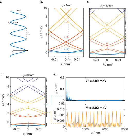
We first investigate the effects of curvature on the eigenenergy spectrum of the nanowire in Fig. 1. When the nanowire is completely flat (i.e., ) and the periodic potential is absent (i.e., ), the system becomes an isotropic SOI electron gas for which the eigenenergies are where denotes that the wavevector in the extended zone scheme and can take values between . Although the flat nanowire is uniform, for the purpose of comparison, it can also be regarded as a periodic system with a period of because . This allows the introduction of a Brillouin zone with the boundaries located at , where (without the tilde) denotes a wavevector in the reduced zone scheme. Note that the dispersion relations for are folded back into the first Brillouin zone, as shown in Fig. 1b. In Fig. 1b, the thicker dispersion curves correspond to the positive eigenspinor branch with energies of where . The fold-back of the dispersion curves to the reduced Brillouin zone leads to crossing points, such as between the th positive and negative eigenspinor branch states, as indicated in the figure.
We now introduce a small curvature () to the nanowire, and plot the resulting dispersion relation in Fig. 1c. The introduction of a periodic curvature modulation to the nanowire opens large anticrossing band gaps at , which mark the crossing points of the positive and negative eigenspinor branches in the absence of curvature. Moreover, the energies of the bands tend to be compressed and shifted downwards along the energy axis. For example, the two bands labelled as iii in Fig. 1c, which span across an energy range of 1.6 meV, originate from the upper half of the bands in Fig. 1a. Originally, these span an energy range of 2.5 meV between 2 meV to 4.5 meV (Fig. 1b), but now span a range of just 1.4 meV between 1.8 to 3.2 meV (Fig. 1c). The compression becomes even more significant for the higher energy bands, as can be seen by comparing the positions of the band gaps in Fig. 1c with the energies of the band crossing points at in Fig. 1b.
We now consider a periodic curved nanowire of a finite length along . Because of the loss of translational invariance, is no longer a good quantum number, and the allowed eigenenergies of the finite-length wire become quantized owing to the quantum confinement effect. The series of dots depicted to the right of Fig. 1c represent the discrete eignenergy spectrum of a nanowire of length . Note that the eigenenergies of the finite curved nanowire fall within the energies spanned by the energy bands of the infinite nanowire. In addition, there are no eigenstates of the finite nanowire that fall within the energy band gaps of the infinite nanowire formed by the curvature-induced anticrossing.
We will now demonstrate the onset of curvature-induced topological states in finite nanowires with periodic curvature of sufficiently large amplitude. Increasing the curvature amplitude results in a further compression of the infinite nanowire bands along the energy axis and a widening of the curvature induced anticrossing band gaps (Fig. 1d). Interestingly, when the band gaps are sufficiently large, mid-gap states may emerge in the corresponding finite nanowire. The dots depicted to the right of Fig. 1d correspond to the discrete eigenenergies of a finite nanowire of length at .. Note the presence of (two) degenerate finite-length eigenstates at in the middle of the bandgap. Such mid-gap states are absent in the finite nanowire with a smaller curvature amplitude of 40 nm, as shown in Fig. 1c. It is interesting to note that the mid-gap state is an edge state with localization near one end of the nanowire. This can be seen from the particle density plotted against the coordinate along the length of the nanowire in Fig. 1e. For comparison, we plot the particle density for one of the finite-length eigenstates corresponding to that lie within one of the bands (indicated by a green dot). In this case, the density profile shows a typical profile that extends throughout the interior of the nanowire. The presence of the mid-gap states with edge localization is an indication of the presence of non-trivial topological states in the curved nanowire, a point which we will subsequently prove by considering their corresponding Chern number.
III.2 Effects of magnetization coupling and periodic potential on eigenenergy spectrum
An adiabatic charge pump can be established by introducing a sinusoidal sliding potential and adiabatically varying the phase difference between the sliding potential and the nanowire curvature. We will show that the amount of charge pumped per period as well as the number of edge states can be tuned by the magnetization . Fig. 2a replicates the dispersion relation of the finite curved wire in Fig. 1d so that the effects of the potential and the magnetization can be more easily seen by comparison. Here, we have focused on a narrower energy range within which the edge states appear, and labelled the bands differently from Fig. 1d to facilitate the discussion that follows.
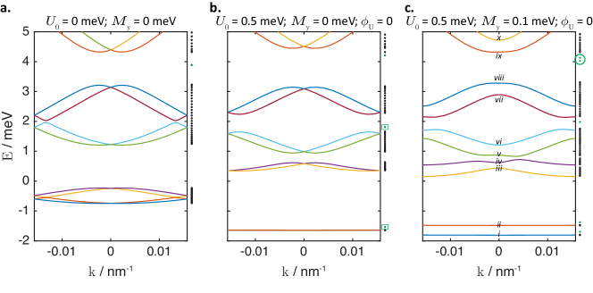
We will now impose a sliding potential on the nanowire with the same periodicity as its curvature, and show that this significantly modifies its bandstructure. The main plot of Fig. 2b shows the bandstructure of an infinite nanowire in the presence of a sliding potential of and zero phase difference (), while the discrete eigenstates of the corresponding finite nanowire of length are depicted to the right side of the plot. Comparing with the bandstructure in the absence of the sliding potential (Fig. 2a), it can be seen that the sliding potential displaces pairs of bands along opposite directions along the energy axis – some pairs are pushed downwards, while others are pushed upwards. This causes a significant widening of the curvature-induced bandgaps. Generally, the sliding potential has a larger effect on lower-energy bands. For instance, the two upper-most bands (labelled and ) are hardly affected by the presence of the potential, whereas there is a dramatic change and displacement of the four lowest bands (labelled to ). This may be attributed to the relative size of the sliding potential compared with the energy of the bands. The sliding potential can also induce a band-gap opening, e.g., an energy gap is now opened between bands and in Fig. 2b where previously no gap was present between the two bands shown in Fig. 2a. Most interestingly, new mid-gap edge states (indicated by the squares in Fig. 2b) also emerge in the energy gaps between bands and , and between bands and .
We now introduce magnetization coupling to the curved nanowire system as another means of modulating its bandstructure. Figure 2c shows the bandstructure of the infinite nanowire and the eigenenergies of the finite-length nanowire in the presence of a magnetization coupling of and the same sliding gate potential as was considered in Fig. 2b. As before, the finite eigenstates of the corresponding finite nanowire with the same magnetization coupling and sliding potential are depicted as dots to the right of Fig. 2c. The five pairs of bands in Figs. 2a and 2b originate from the SOI spin-split eigenspinor branches in the flat uniform nanowire system in Fig. 1b, as we have explained earlier. For example, band () originates from the negative (positive) eigenspinor branch of the bands of the flat nanowire. Note that for each pair, the bands are two-fold degenerate at where the SOI-induced splitting of the bands is zero. The application of the magnetization coupling lifts the degeneracy at . For the finite curved nanowire, the energy degeneracy of the eigenstates is also lifted. Note that each of the dots in Fig. 2a and 2b actually represents two degenerate states and these are split in the presence of finite coupling. Thus, there are now two distinct energy values of the mid-gap states between bands and , and , and and instead of a single energy value previously . (The energy splitting between the mid-gap states is most obviously seen in the and pair of mid-gap states in Fig. 2c (circled) and is not readily visible at the scale of the figure for the remaining lower-energy pairs. ) Due to the energy splitting of the spin-split pairs arising from the magnetization coupling, alternate pairs of bands experience energy shifts of opposite signs. This opposite displacement in energy leads to a narrowing of the energy bandgaps, e.g., the gap between bands and . It is conceivable that as the magnetization coupling is increased further, the bands may cross each other in energy. Significantly, such band inversions are typically associated with topological phase transitions. We shall later show that this band inversion can indeed occur and result in a “transfer” of discrete Chern numbers between the bands that touch. Thus, magnetization coupling does not just act as an additional knob to modulate the energy dispersion of the curved nanowire system but can be applied to switch its topological properties.
III.3 Charge pumping and Chern number in curved nanowire system
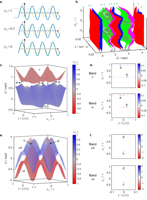
Finally, we consider another parameter which is the phase between the nanowire curvature and the sliding potential . This allows us to define a two-dimensional parameter space in conjunction with the wavevector , and thus characterize the topological properties of the curved nanowire system. Fig. 3a schematically shows the displacement of with respect to as the phase difference as is increased. Fig. 3b shows how the bandstructures of the infinite nanowire system in Fig. 2c vary with . Although the energy ranges spanned by the infinite wire bands may overlap as is varied, the bands do not, in general, touch one another. The absence of energy degeneracy between the different bands in the space allows us to define a topological Chern number in that space for each band as
| (14) |
where is the th band, and is the Berry curvature of this band, and is turn given by
| (15) |
Here, is the eigenstate of the th band and is a function of both and , and is its Chern number. The resulting Chern numbers for each of the bands in Fig. 3b are labelled on top of the band.
It is necessary to understand the distribution of the Berry curvatures amongst the bands in order to explain the variation of the band Chern numbers with the applied magnetization. We therefore focus on two pairs of bands, namely, bands and , and bands and . The energies of these two pairs of bands are plotted in the surface plots in Fig. 3c and Fig. 3e, respectively, while the Berry curvature distributions of the corresponding bands on the plane are plotted in Fig. 3d and Fig. 3f. Consider bands and in Fig. 3c first. There are two points labelled as and at which the two bands nearly touch (the point appears at both the left and right edges of the plot because the band-touching point is on the Brillouin zone boundary in the plot). These points originate from the anti-crossing points labelled as in Fig. 1b at which the successive bands are closest in energy from one another. Fig. 3d shows that the Berry curvatures in bands and are concentrated around these nearly-touching points, and that the Berry curvatures at a given point, say , have opposite signs on the two bands. These trends can be explained by an alternative expression for the Berry curvature
| (16) |
It is evident that the amplitude of Berry curvature increases sharply as the energy difference between the bands decreases, and that the contributions of the band to the Berry curvature of band (i.e., the term being summmed in Eq. with , ) has an opposite sign from the contribution of band to the Berry curvature of band . We can also observe in Fig. 3f the same tendencies for the Berry curvatures to be concentrated at the nearly touching points ( and ) between two adjacent bands and and the opposite signs of the Berry curvatures of the two bands.
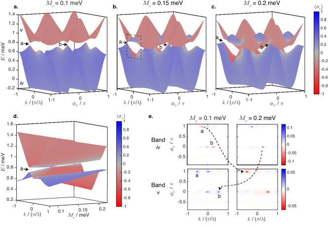
The distributions of the Berry curvatures across the bands change with the variation of as adjacent bands touch and overlap with each other. We have seen earlier in Fig. 2c that as is increased, the bands polarized in the direction are pushed up in energy, while those polarized in the direction are pushed down in energy. This may then result in bands with opposite signs of spin polarization coming into contact with one another. Fig. 4 explains the manner in which the energies and Berry curvature distribution of two adjacent bands change when the bands come into contact. Fig. 4a reproduces the energy distribution of bands and at meV shown in Fig. 3c. The colors of the eigenenergy surfaces indicates the spin polarization of the bands. When is increased to 0.15 meV, as shown in Fig. 4b, band (which has a largely positive spin polarization) is pushed upwards in energy, while band (which has largely a negative spin polarization) is pushed downwards in energy, causing the two bands to approach each other. The shifts in the energies of bands and is perhaps most evident from the band bottom of band and the band top of band , which are cropped off in Fig. 4a (notice that the bands terminate on the planes at the top and bottom of the surface plots in straight lines) but are now visible in Fig. 4b for the same energy range (notice that the top of band and bottom of band now terminate in smooth curves in the range shown). Notably, there are also small regions centered around in the figure (one of which is indicated by the dotted box in Fig. 4b), at which the spin polarization of the two bands differ from that of their surrounding regions.These regions can be interpreted as the interpenetration of the peak regions of band into band , and the trough regions of band into band separated by anti-crossing energy gaps.
These gaps may close at the nearly-touching points and with the variation of . A comparison between Fig. 4a and Fig. 4b shows that the energy gaps between bands and at points and decrease with the increase of from 0.1 meV to 0.15 meV such that and the two bands seem almost touch each other at points and in Fig. 4b. A further increase in , as shown in Fig. 4c for meV, causes the two bands to further interpenetrate into each other, as can be seen from the increase in the negative (positive) spin -polarized region in band (). The energy separations between the two bands at points and have also increased compared to the separation in Fig. 4b, indicating that the bands touch only at isolated values of . This is shown in Fig. 4d, where the is fixed to correspond to that of point while is varied. It can be clearly seen that as increases, the energy separation between bands and initially decreases, becomes 0 (where the two bands touch at meV) , and then increases again. An exchange of the Berry curvatures occurs between the bands in which the Chern number of one band increases by 1 and that of the other band decreases by 1 when the two bands touch each other [41], as shown in Fig. 4e. At meV (left columns), the Berry curvatures around points and are negative in band , and positive in band . The two bands touch at point at meV and at point at meV and swap their Berry curvatures at these touching points. Thus, at meV, the Berry curvatures around points and become positive in band , and negative in band ( as shown in Fig. 4e ), and the Chern number of the band () correspondingly changes from -1 (+1) at meV to +1 (-1) at meV.
III.3.1 Energy dispersions of finite nanowires
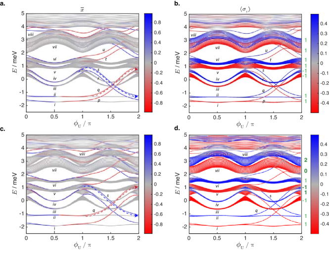
The changes in the Chern numbers of the bands as they come into contact with one another with the variation of are reflected in the dispersion of the energies with and the edge states that emerge in finite nanowires. In Fig. 5a–d the eigenenergy dispersions are plotted as functions of for finite nanowire systems of 20 periodic units. The colors of the lines Fig. 5a indicate the normalized position where is the length of the nanowire, is the position operator, and is an eigenstate of the finite-length nanowire which spans from to . An eigenstate with a value of nearly 1 (-1) therefore indicates a topological edge state which is localized near the right (left) edge of the nanowire (e.g., the upper right plot in Fig. 1d). Conversely, a value of nearly 0 indicates a bulk state (e.g., the lower right plot in Fig. 1d) where the probability distribution of the state is more symmetrically distributed about the centre of the nanowire. Plotting the energy dispersion of the finite nanowire with also allows the origin of its energy bands to be traced more easily. For example, there are two distinct but overlapping groups of bulk states in the finite nanowire lying between 2 to 4 meV (Fig. 5a). (We shall use “band” to refer to each band in the infinite nanowire, and “group” to refer to the group of bulk bands in the finite wire that result from the quantization of each infinite wire band.) These groups of bulk states can be traced to the bands and of the infinite nanowire (Fig. 4b). Although the energy range spanned by the two bands of the infinite nanowire overlap, they do not actually touch anywhere in the Brillouin zone. Likewise, the corresponding bands in the finite nanowire of Fig. 5a also overlap in energy but do not form any anticrossing. Consequently, we can label each group of bulk states of the finite nanowire in Fig. 5a with the same Roman numeral index of the infinite nanowire band which they originate from, along with the Chern number of the band in Fig. 5b.
In order to further differentiate the different bulk bands of the finite nanowire as well as analyze the effect of the magnetization coupling , we plot the spin expectation value corresponding to each state (Fig. 5b). As we have described earlier, in the infinite nanowire, the effect of the coupling is to further split the spin-split SOC bands, such that states with negative (positive) spin polarization will be pushed downwards (upwards) in energy. Hence, in the finite nanowire dispersion of Fig. 5b, group which has a negative spin polarization (reddish colour) is pushed below in energy compared to group which has a positive polarization (bluish colour) relative to their original energies when the coupling was absent. Thus, generally, the effect of coupling produces pairs of groups of bands in the finite-length nanowire with alternating signs of the spin polarization, with the groups labelled by odd (even) Roman numerals being polarized along the negative (positive) spin polarization.
The combination of finite Chern numbers and the presence of boundaries leads to the emergence of edge states in finite nanowires. These edge states are localized near the left (red lines) or right (blue lines) edge of the nanowire and are labelled to (Fig. 5a). The energies of these edge states span the energy gaps between the groups of bulk states as is varied from 0 to . For example, consider the edge states and , which connect groups and , in Fig. 5a. Within some range of values of , this edge states may penetrate into the bands and of bulk states, respectively, but emerge from these bands more or less intact with the further increase of , before eventually merging into their destination bands. As increases from 0 to , the edge state , which is localized on the right edge, gets detached from band and decreases in energy and eventually joining band . Conversely, the edge state , which is localized on the left edge, increases in energy and leaves band to join band . The physical interpretation of these band-gap crossings by the pair of edge states is as follows: As is adiabatically varied from to , a charge in edge state localized on the right is removed from band while a charge in edge state which is localized on the left is brought from band to band to replace it. This results in the net movement of a charge from the right edge of band to the left edge as is varied over a period (from 0 to ). Hence, band thus has a Chern number of -1 (Fig. 5b). Likewise, the Chern numbers of the other bands can be related to the transport of the edge states via the evolution of over a complete period.
We now turn our attention to the effects of increasing the coupling on the dispersion spectra as well as the topological properties of the bands. Figs. 5c and Fig. 5d are analogous to Fig. 5a and 5b except that the magnetization coupling is increased to = 0.2 meV. As we have seen earlier in Fig. 4a and Fig. 4c, increasing from 0.1 meV to 0.2 meV results in interpenetration between bands and bands . The interpenetration of the two bands is manifested by the sign reversal of the spin expectation values of the two corresponding groups of bands in the finite wire (comparing Fig. 5b and Fig. 5d) at and , which respectively correspond to the projections of point and onto the axis, respectively. As we have also seen in Fig. 4e, the increase in changes the Chern numbers of groups and in the finite wire. This change is reflected in the trajectories of the edge states among the bulk bands in the dispersion of the finite wire. For example, edge state , which passes from group and enters and subsequently exists group as shown in Fig. 5a. At the larger value of meV, state is now completely contained within group (see Fig. 5c) for due to the exchange of the Chern numbers between bands and at the touching point on the (see Fig. 4e) . Similarly, edge state , which terminates in group at in Fig. 5a at the lower value, now terminates inside group at at the higher value (Fig. 5c) due to the exchange of the Chern numbers between bands and at point on the plane (see Fig. 4e).
The exchange of the Chern numbers between adjacent bands also has a significant impact in the spin polarization of the eigenstates in Fig. 5b and Fig. 5d. At the lower value of 0.1 meV, the edge state and emerge from the vicinity of the peaks of group at and , respectively. The peak region of group have a positive spin polarization. At the higher value of 0.2 meV, the peak regions of group have “broken away” from band from band and become embedded into group (denoted by blue regions in Fig. 5d). The regions that have broken off carry along with them the end points of the state bands and along with them so that these states now terminate in group rather than group . Similarly, groups and have also undergone a change in Chern numbers and their related edge states when was increased from 0.1 meV to 0.2 meV (compare Figs. 5a and 5b with Figs. 5c and 5d). Here, the upward (downward) shift of group () results to the emergence of a distinct band gap between the groups in which edge states now emerge.
III.3.2 Tuning of Chern numbers by magnetization magnitude and direction
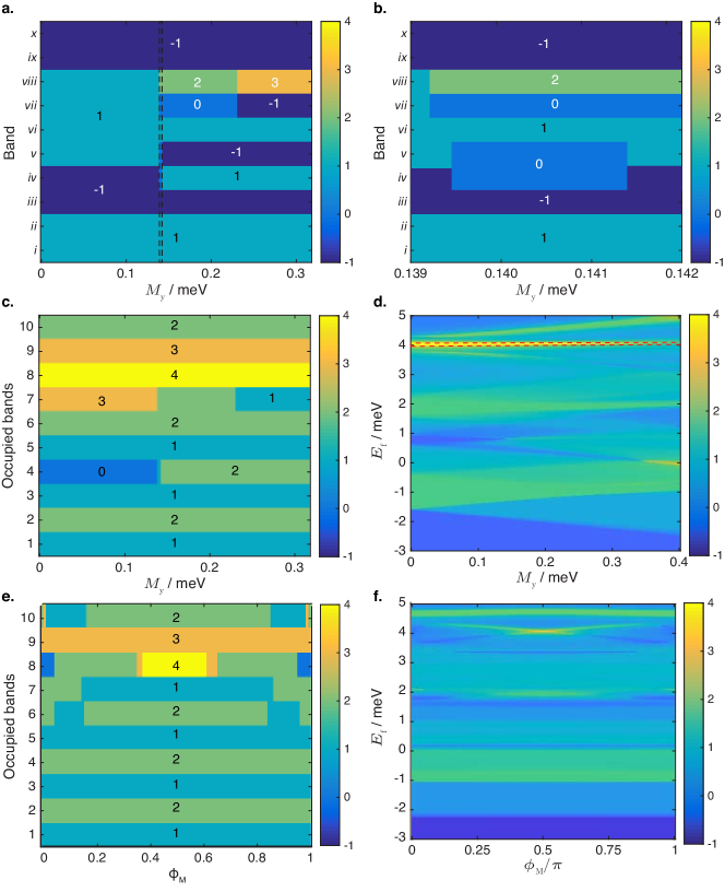
We further investigate the evolution of the Chern numbers with the variation in the magnetization (see Fig. 6a). The values of the Chern numbers change by 1 when adjacent pairs of bands come into contact with or move apart from each other with increasing . A magnified view of Fig. 6a for the range of 0.139 meV to 0.142 meV is shown in Fig. 6b to show that the Chern numbers of bands and are both zero over a finite range of . The range spans from meV, at which bands and first touch at point on the plane, to meV when the two bands touch again at point . At both of these points, a unit of Chern number is transferred between the two bands.
As a different example, we can consider the transfer of Chern number between bands and . Bands and initially overlap with each other. As is increased, the two bands move apart (cf. Figs 5a and 5b). A band touching point occurs at point on the plane (Fig. 3e) at meV, at which one unit of Chern number is transferred from band to band . A second transfer of Chern number between bands and occurs at meV, at which a touching point appears at point on the plane.
One distinct characteristic that can be observed is the large value of Chern number that can be associated with a particular band, i.e., up to a value of 3. This is attributed to the presence of multiple bands (in principle, infinite in number) in the periodically curved nanowire system due to the folding of the Brillouin zone. The multiplicity of bands allows an individual band to successively accumulate units of Chern numbers as touching points occur between adjacent pairs of bands with the increase in . For example, the Chern number of band in Fig. 6a has an initial Chern number of 1 which increases in two successive steps to 3 with the increase in . Such a large Chern number states is not observed in typical two- or four-band topological systems such as the BHZ Hamiltonian for 2D topological insulators [18] due to their fewer number of bands. The total number of charges pumped across any point in the infinite nanowire system by the adiabatic variation of from 0 to is given by the sum of the Chern numbers of the occupied bands. We therefore show the cumulative sum of the Chern numbers from the lowest energy band up to the highest occupied band index for each value of in Fig. 6c. These results show that for a fixed number of occupied bands, the number of charges pumped across the system can be varied simply by tuning the strength of the magnetization coupling. For example, when seven bands are occupied, the Chern number can be successively reduced from 3 to 2 and then to 1 by increasing from 0 to beyond 0.23 meV. Since the Chern number is linked to the number of pumped charges per adiabatic cycle of the sliding potential, one can in principle achieve a discrete and topologically robust charge transfer, by modulating the magnetization coupling. This may find use in a magnetic memory application in which in which the value of the bit is represented by the Chern number [38, 39, 40].
It is more practicable however to control the Fermi level of the system rather than the scenario of having a certain number of fully-occupied bands and having no partially occupied ones. Hence, in Fig. 6d, the cumulative Chern number is plotted as a function of Fermi energy , taking into consideration all occupied states lying below and including the contribution to the Chern number from the partially occupied bands. Here, the sums of the Chern numbers are not necessarily whole integers as the Fermi energy may cut across partially occupied bands. We observe that the boundaries between regions with different cumulative Chern numbers form a linear variation with respect to . This is due to the fact that these boundaries are dependent on the energy of the band minima (at which successive bands emerge and start to contribute to the Chern number), and these vary linearly with . Furthermore, the distinct regions in Fig. 6d with different cumulative Chern number can be mapped to the corresponding region in Fig. 6c. For example, the region around meV in Fig. 6d indicated by the red dotted quadrilateral with the Chern number of 4 corresponds directly to the occupany of eight bands in Fig. 6c.
Besides modifying the strength of the magnetization coupling, an alternative and perhaps easier method to tune the Chern number is by varying its direction. We plot in Fig. 6e and Fig. 6f the cumulative Chern number as a function of the number of occupied bands and for the same system, except that the direction of the magnetization coupling is varied on the - plane while keeping the coupling strength constant (at 0.3 meV), i.e., . As a result, the cumulative sum of the Chern numbers will also vary with the magnetization orientation denoted by . Fig. 6f shows that when the Fermi energy is set to around 4 meV, the Chern number and hence the number of charges pumped per adiabatic cycle can be varied drastically between zero to four by varying the magnetization angle. Hence, by setting the at an appropriate value and using as an input variable, one can thus control the discrete number of pumped charges per phase period as a topologically robust output.
IV Conclusions
In this work, we showed that the topological properties of a one-dimensional nanowire may be modified through the introduction of a periodic curvature, sliding potential and magnetization coupling. We described a scheme for obtaining the finite difference approximation to the Hamiltonian of a one-dimensional curved nanostructure in the presence of spin-orbit interaction (SOI). We showed that the initial dispersion with the SOI-induced split may be further modified with the addition of the magnetization coupling. This has the effect of modifying the ordering and energy gap of the different bands. Further tuning of the dispersion is possible by introducing a sliding potential and varying the phase difference between it and that of the periodic curvature. More importantly, the presence of provides an additional parameter to obtain a well-defined invariant or Chern number which characterize the topological state of the system. By aligning the Chern number to the sliding potential, we are also able to link this invariant to a physical process, i.e., the number of discrete charges being pumped across the curved nanowire per adiabatic period of the sliding potential. The number of pumped charges therefore serve as a measurable indicator of the underlying topology of the system. We find that the multiplicity of bands in the system due to its periodicity and successive splits via SOI and magnetization coupling, allows the realization of states or bands with high Chern number. We showed that these distinct bands are connected by robust edge states which are localized at the boundaries, and which have the effect of transporting discrete states from one band to another, leading to shifts in the Chern number. The band and edge state profiles can be modulated by the strength and direction of the magnetization coupling, as well as the number of occupied bands (which in turn depends on the Fermi level) based on realistic parameter values. This opens the way for the system to be utilized for a multi-state memory application with topologically robust, discrete-valued readout value and having multiple levers of control.
V Acknowledgements
We thank Prof. C.-R. Chang and R.-A. Chang at the National Taiwan University for helpful discussions during the course of this project. This work is supported by the Singapore National Research Foundation (NRF), Prime Minister’s Office, under its Competitive Research Programme (NRF CRP12-2013-01, NUS Grant No. R-263-000-B30-281), Ministry of Education (MOE) Tier-II Grant MOE2018-T2-2-117 (NUS Grant Nos. R-263-000-E45-112/R-398-000-092-112), MOE Tier-I FRC Grant (NUS Grant No. R-263-000-D66-114), and other MOE grants (NUS Grant Nos. C-261-000-207-532, and C-261-000-777-532).
References
- [1] K.-C. Chen and C.-R. Chang, Geometrical effect on spin transport, Spin 3, 1340006 (2013).
- [2] J.-S. Jeong, J. Shin and H.-W. Lee, Curvature-induced spin-orbit coipling and spin relaxation in a chemically clean single-layer graphene. Phys. Rev. B 84, 195457 (2011).
- [3] F. E. Meijer, A. F. Morpurgo, and T. M. Klapwijk, One-dimensional ring in the presence of Rashba spin-orbit interaction: Derivation of the correct Hamiltonian, Phys. Rev. B 66, 033107 (2002).
- [4] J.-Y. Chang, J.-S. Wu, and C.-R. Chang, Exact Hamiltonians with Rashba and cubic Dresselhaus spin-orbit couplings on a curved surface, Phys. Rev. B 87, 174412 (2013).
- [5] Z.-J. Ying, P. Gentile, C. Ortix, and M. Cuoco, Designing electron spin textures and spin interferometers by shape deformations, Phys. Rev. B 94, 081406 (2016).
- [6] A. Bringer and Th. Schäpers, Spin precession and modulation in ballistic cylindrical nanowires due to the Rashba effect, Phys. Rev. B 83, 115305 (2011).
- [7] T.-C. Cheng, J.-Y. Chen, and C.-R. Chang, Geometrical effect on the non-Abelian spin-orbital gauge field of a curved surface, Phys. Rev. B 84, 214423 (2011).
- [8] M.-H. Liu, J.-S. Wu, S.-H. Chen, and C.-R. Chang, Spin and charge transport in U-shaped one-dimensional channels with spin-orbit couplings. Phys. Rev. B 84, 085307 (2011).
- [9] E. Zhang, S. Zhang, and Q. Wang, Quantum transport in a curved one-dimensional quantum wire with spin-orbit interactions, Phys. Rev. B 75, 085308 (2007).
- [10] Z. B. Siu, M. B. A. Jalil, and S. G. Tan, Semicircular Rashba arc spin polarizer, J. Appl. Phys. 115, 17C513 (2014).
- [11] K. S. Das, D. Makarov, P. Gentile, M. Cuoco, B.J. van Weees, C. Ortix, and I.J. Vera-Marun, Indepdent geometrical control of spin and charge resistances in curved spintronics, Nano Lett. 19, 6839 (2019).
- [12] F. Santos, S. Fumeron, B. Berche, and F. Moraes, Geometric effects in the electronic transport of deformed nanotubes, Nanotechnology 27, 135302 (2016).
- [13] R. Cheng, Y.-L. Wang, H. Jiang, and X.-J. Liu, Geometric effects of a quarter of corrugated torus, Condens. Matter 4, 3 (2019).
- [14] W.-R. Cao, Y.-L. Wang, X.-L. Chen, H. Jiang, C.-T. Xu, and H.-S. Zong, The geometric potential of a double-frequency corrugated surface, Phys. Lett. A 383, 2124 (2019).
- [15] Y.-L. Wong, G.-H. Liang, H. Jiang, W.-T. Lu, and H.-S. Zong, Transmission gaps from corrugations, J. Phys. D: Appl. Phys. 49, 295103 (2016).
- [16] S. Ono and H. Shima, Tuning the electrical resistivity of semiconductor thin films by nanoscale corrugation, Phys. Rev. B 79, 235407 (2009).
- [17] Z. B. Siu, M. B. A. Jalil, and S. G. Tan, Curvature induced out-of-plane spin accumulation in Rashba quantum waveguides, J. Appl. Phys. 121, 233902 (2014).
- [18] B. A. Bernevig, T. L. Hughesm and S.-C. Zhang, Quantum spin Hall effect and topological phase transition in HgTe quantum wells, Science 314, 1757 (2006).
- [19] M. Konig et al., Quantum spin Hall insulator state in HgTe quantum wells, Science 318, 766 (2007).
- [20] D. J. Thouless, M. Kohmoto, M. P. Nightingale, and M. den Nigs, Quantized Hall conductance in a two-dimensional periodic potential, Phys. Rev. Lett. 49, 405 (1982).
- [21] C. L. Kane and E. J. Mele, topological order and the quantum spin Hall effect, Phys. Rev. Lett. 95, 146802 (2005).
- [22] M. Z. Hasan and C. L Kane, Colloquium : Topological insulators, Rev. Mod. Phys. 82, 3045 (2010).
- [23] J. E. Moore, The birth of topological insulators, Nature, 464, 194 (2010).
- [24] X.-L. Qi and S.-C. Zhang, Topological insualtors and superconductors, Rev. Mod. Phys. 83, 1057 (2011).
- [25] Z. B. Siu, J.-Y. Chang, S. G. Tan, M. B. A. Jalil, and C.-R. Chang, Curvature induced quantum phase transitions in an electron-hole system, Sci. Rep. 8 (2018).
- [26] P. Gentile, M. Cuoco, and C. Ortix, Edge states and topologicial insulating phases generatred by curving a nanowire with RSOC, Phys. Rev. Lett. 115, 256801 (2015).
- [27] S. Pandey, N. Scopigno, P. Gentile, M. Cuoco, and C. Ortix, Topologcial qunatum pump in serpentine-shaped semiconducting narrow channels, Phys. Rev. B 97, 241103 (2018).
- [28] J. Wang, J. F. Liu, and C. S. Ting, Topologcial two-parameter charge pump in a one-dimensional semiconductor nanowire superlattice, Phys. Rev. B 100, 075402 (2019).
- [29] T. Fujita, M. B. A. Jalil, S. G. Tan, and S. Murakami, Gauge fields in spintronics, J. Appl. Phys. 110, 121301 (2011).
- [30] S. G. Tan, S.-H. Chen, C. S. Ho, C.-C. Huang, M. B. A. Jalil, C. R. Chang, and S. Murakami, Yang-Mills physics in Spintronics, Phys. Rep. 882, 1 (2020).
- [31] R. da Costa, Quantum mecahnics of a constrained particle, Phys. Rev. A 23, 1982 (1981).
- [32] H. Jensen and H. Koppe, Quantum mechanics with constraints, Ann. Phys. 63, 586 (1971).
- [33] Y. Sun, W. M. Choi, H. Jiang, Y. Y. Huang, and J. A. Rogers, Controlled buckling of semiconductor nanoribbons for stretchable electronics, Nat. Nanotech. 1, 201 (2006).
- [34] J.-S. Heron, C. Bera, T. Fournier, N. Mingo, and O. Bourgeois, Blocking phonons via nanoscale gemoetrical design, Phys. Rev. B 82, 155458 (2010).
- [35] M.-C. Hsu, L.-Z. Yao, S. G. Tan, and M. B. A. Jalil, Inherent orbital spin textures in Rashba effect and their implications in spin-orbitronics, J. Phys: Condens. Matter 30, 285502 (2018).
- [36] J. Nitta, T. Akazaki, H. Takayanagi, and T. Enoki, Gate control of spin-oribit interaction in an inverted heterostructure, Phys. Rev. Lett. 78, 1335 (1997).
- [37] J. Luo, H. Munekata, F. F. Fang, and P. J. Stiles, Effects of inversion asymmetry on electron energy band structures in GaSb/InAs/GaSb quantum wells, Phys. Rev. B 41, 7685 (1990).
- [38] M. B. A. Jalil, S. G. Tan, and Z. B. Siu, Quantum anomalous Hall effect in topological insulator memory, J. Appl. Phys. 117, 17C739 (2015).
- [39] T. Fujita, M. B. A. Jalil, and S. G. Tan, Topological insulator cell for memory and magnetic sensor applications, Appl. Phys. Express 4, 094201 (2011).
- [40] M. B. A. Jalil and S. G. Tan, Robustness of topological Hall effect of nontrivial spin textures, Sci. Rep. 4, 5123 (2014).
- [41] R. Roy, classification of quantum spin Hall systems : An approach using time-reversal invariance, Phys. Rev. B 79, 195321 (2009).