Revisiting Residue Codes for Modern Memories
The latest and authoritative version of the document is published here: https://ieeexplore.ieee.org/document/9923862
Abstract
Residue codes have been traditionally used for compute error correction rather than storage error correction. In this paper, we use these codes for storage error correction with surprising results. We find that adapting residue codes to modern memory systems offers a level of error correction comparable to traditional schemes such as Reed-Solomon with fewer bits of storage. For instance, our adaptation of residue code – MUSE ECC – can offer ChipKill protection using approximately 30% fewer bits. We show that the storage gains can be used to hold metadata needed for emerging security functionality such as memory tagging or to provide better detection capabilities against Rowhammer attacks. Our evaluation shows that memory tagging in a MUSE-enabled system shows a 12% reduction in memory bandwidth utilization while providing the same level of error correction as a traditional ECC baseline without a noticeable loss of performance. Thus, our work demonstrates a new, flexible primitive for co-designing reliability with security and performance.
Index Terms:
error correcting codes; memory tagging; metadata; rowhammerI Introduction
Error Correcting Codes (ECCs) are a standard technique for improving system reliability and are widely used today. ECCs improve reliability by encoding data in a redundant format that uses additional bits of information to identify and correct data bits that change while in storage or transit. To minimize storage and transmission overheads, codes that use fewer redundancy bits for a desired level of reliability and are easy to implement have gained widespread use.
Residue codes are a specific type of ECC used for detecting and correcting errors that happen during computation[5, 59] and were developed in the 1960-70s[30, 16, 71]. Unlike storage-oriented codes like Reed-Solomon codes[65], residue codes have a nice property that the error correction information can be computed in parallel with computational operations: say is the ECC function, and is the computational function, then for residue codes, for some common functions . In contrast, for storage-oriented codes, can be calculated only after is computed[59].
In this work, we present MUSE, our adaptation of the residue codes that provides a level of protection similar to storage-oriented codes but with fewer bits of storage. These saved bits can be used for storing metadata in a manner that also protects the metadata itself. As compute and memory are merging[50], and security and reliability place more demands on memory[68, 37, 3], codes, such as MUSE, not only offer a path for better integration of both the compute and memory components but also enable techniques that need metadata to improve security or performance.
Residue codes are easy to explain. To protect the data, we multiply it with a deliberately chosen multiplier before storing it in memory. When the data is retrieved from memory, we divide the value by the same chosen multiplier. If there are no errors between the storage and retrieval, we should get a remainder of zero. If some bits are flipped, we use the remainder to locate the bits that need to be corrected[30].
To use the remainders to correct a flipped bit, we need each remainder to have a one-to-one mapping with the error that occurred in that bit. Hence, we enumerate all possible error patterns, compute their values, and search for a multiplier that leaves a unique remainder for each error. A good multiplier is the smallest integer number that satisfies the unique remainder property, as a smaller number requires fewer redundancy bits.
One challenge with adopting the above code to memory is that memory has to accommodate failure models where multiple bits can fail. In this case, the number of remainders grows exponentially with the number of errors, and the multiplier values become too large for practical use[56, 8]. To overcome this problem, we invent a new optimization technique we call shuffling. As the name suggests, shuffling changes the bit positions of the data before it is written to memory, which changes the distribution of values representing the errors and their remainders. With shuffling, we can evaluate the same multiplier multiple times, increasing the chance of finding a multiplier that gives unique remainders.
Another challenge with using this code for memory systems (or even compute systems) is that a naïve implementation will be prohibitive in terms of performance as it requires expensive multiplication and division operations on the critical path delaying memory reads and writes. For instance, using division can take up to 70 cycles [24]. We show that we can avoid these costs using two optimizations: First, the MUSE multiplier is fixed and known at design time which allows us to avoid the cost of general multipliers and dividers. We find that specialization of these circuits can reduce the latencies to about three cycles. Second, we use a systematic encoding of the codes that mitigates the critical path latency of these workloads.
With these optimizations, we adopt residue codes to modern memory systems and compare them to the ChipKill scheme based on the Reed-Solomon codes with the redundancy of commercial schemes [4, 31] and demonstrate the following benefits:
-
•
MUSE uses fewer bits of storage than comparable ChipKill schemes. MUSE corrects multi-bit errors confined to a single DRAM chip on a DIMM, allowing the system to withstand a permanent memory chip failure with at least four fewer redundancy bits than ChipKill codes used in enterprise systems[4, 31]. We show how these saved bits can be used to implement ARM Memory Tagging Extensions[3], saving up to 3% of DRAM power consumption, and how the bit savings can be used to store cryptographic hashes that reduce the probability of successful Rowhammer[23] attack to .
-
•
MUSE is a single code that can guarantee the correctness of both data in storage and during computation. MUSE is a promising fit for Processing In-Memory – a new emerging technology where computation happens near the data in memory[50]. We show that in the settings of PIM-enabled HBM2, MUSE could use fewer redundancy bits than the provisions specified in the standard while protecting the data during both the storage and the computation without the need for multiple reliability schemes.
-
•
MUSE ECC is more flexible. MUSE’s codewords division between the redundancy and data is tunable at single-bit granularity for any symbol size. This flexible division allows to design a code with a specific target for the spare storage. We show that for multiple configurations of the codeword, data, and redundancy lengths, MUSE provides ChipKill guarantees, while Reed-Solomon does not due to its fixed two-symbol redundancy.
-
•
MUSE offers customization of codes to fit error models. We show how we can cover two classes of errors simultaneously: (1) single-bit errors and (2) asymmetrical multi-bit errors (i.e., errors due to lack of refresh) confined to a single DRAM chip on a DIMM. We showcase MUSE code for this model, which uses 13 check bits leaving three bits for other uses.
The rest of the paper is organized as follows: Section II provides an overview of residue codes, Section III describes the construction of MUSE, Section IV presents some practical codes, Section V details the microarchitecture, Section VI presents the uses cases, and in Section VII we evaluate the overheads of MUSE and compare to Reed-Solomon codes. We discuss related work in Section VIII and conclude with Section IX.
II Background
In this section, we briefly cover the formulation of the residue codes. We discuss residue code construction, including its systematic formulation, and the mapping of errors to remainders.
Code Construction The following equations describe how is encoded into a codeword, how a codeword is decoded back into , and how the errors are detected and corrected:
| (1) |
| (2) |
| (3) |
The is encoded to the by multiplying by a whole number m (Eq. 1). Upon reading the , we compute the remainder of the divided by m (Eq. 2). If the remainder is zero, we can recover the original data by simply dividing the codeword by m (error-free case); otherwise we subtract the derived from remainder to correct the and then recover the data by dividing by m (Eq. 3). For this scheme to work, we pick so that each remainder corresponds to one error only, allowing for unambiguous error correction.
The construction above presents a serious problem—the original data is available only after division. This can introduce a steep penalty because of the latency of the division. To avoid this steep penalty for the common case of no errors, we can use a simple math trick developed by Chien in 1964 [16]. Chien proposed to separate the from the redundancy by shifting the in the left by bits such that the remaining bits can be used to store a special value , which is chosen in such a way so that the as shown in Eq. 4:
| (4) |
This way, the data in the codeword are easily separated from the redundancy, i.e., , and no integer division is required to recover the data. We will use this formulation as a basis for MUSE so that the data and the error correction bits can be stored separately (also known as “systematic” encoding).
Mapping Remainders to Bit Positions Next we will describe how single-bit errors are handled. When an error flips bits, it transforms the codeword into another codeword. The difference between the original and erroneous codeword is what we refer to as the error value. However, unlike in traditional codes where single bit flip corresponds to a single error value, in residue codes, each bit flip has two error values: one for 01 bit flips and the other for 10 bit flips.
As an illustration, let us look into an example. Say, the integer value is the codeword. Its binary representation is: . Now assume that bit (in bold) is flipped and codeword value becomes or , leading to the error value of . Now let us assume that the codeword is or . If the same bit was flipped 01, corrupting the codeword to be , the error value would be . Hence, any single bit error may have two distinct error values, and the value itself depends on the direction of the bit flip. To identify the corrupted bit and correct its value, every bit in the word requires two distinct remainders. Note that both of those error values are integers powers-of-two: and . Hence, in general, error at bit has error values of , where a positive value is for bit error 01, and a negative value is for the error 10.
III MUSE
The material presented in the previous section was developed back in the 1960s and 70s in the context of computers that featured arithmetic units111Caches were invented in 1965[78] and DRAM in 1967[22]. While the math works well for memories too, directly applying the ideas to memories is not straightforward. For instance, just being able to support single-bit errors is not very useful for memory errors; we need multi-bit error support as these errors are common enough to warrant support for a large class of systems. However, introducing multi-bit error support (naively) increases the storage requirements of the code [56, 8], making it less competitive with modern codes. In this section, we build upon the construction from the previous section and extend residue codes to fit modern memory systems.
III-A Mapping Remainders to Symbol Errors
We start by extending the residue codes to protect against multi-bit errors confined to a single -bit-wide DRAM device. We are interested in this class of errors because codewords are striped across multiple DRAM chips on a DIMM, and if one chip fails, the corresponding part of the codeword will exhibit an -bit error. Hereon, we define a symbol as a group of bits written to a single DRAM device. Each -bit symbol may have possible errors— same as the number of ways for one -bit number to become a different -bit number. For example, for 4-bit symbols, a 4-bit value can be corrupted via 30 different errors, i.e., to become a value other than the original. Some of these error values are positive while others are negative. If the initial data value was , it could have only 15 positive errors, while would have three positive and twelve negative error values.
III-B Shuffling
However, with the symbol error model, the amount of errors in the code increases significantly. This increase, in turn, leads to a higher chance that multiple errors will result in identical remainders, making it impossible to differentiate between them for correction. To overcome this issue, we introduce shuffling—a new technique that reduces the chance of different errors having the same remainder.
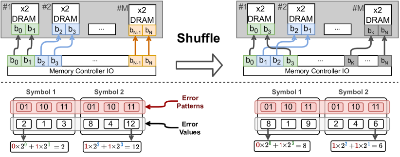
We explain shuffling and its benefits with a simple example. The top portion of Figure 1(a) shows a toy example where the memory controller writes the data in a shuffled manner into a DIMM with x2 DRAM devices. In this example, codeword bits and are written into DRAM device , bits and are placed in device , etc. The bottom portion of the figure shows how shuffling affects the numerical range of the error values (for convenience, only the positive values are shown): the error values of the first symbol are 1, 8, or 9, while the error values for the second are 2, 5, or 6. For instance, for the first symbol, the error value of error pattern changes from to (see the equations in the figure). As a result, with shuffling, the numerical range of error values changes from [1,12] to [1,9]. Thus, shuffling results in a different set of error values, increasing our chances that a given multiplier can be used to disambiguate the error patterns.
Mapping Remainders to Shuffled Symbol Errors With shuffling, an -bit symbol error is transformed from a sequential -bit error into single-bit errors. Continuing with our example, failure of DRAM in Figure 1(a) results in corruption of bits and as opposed to and for the un-shuffled case. Generalizing, the -bit shuffled symbol error may have one of the possible error values. For example, the first symbol of a codeword from Figure 1(a), with bits and , has six possible error values: , and . After shuffling, this symbol stores bits and and has eight possible error values: , and . Despite the increase in the number of error values per symbol, shuffling enables codes that cannot be defined with the traditional residue code construction (Section IV).
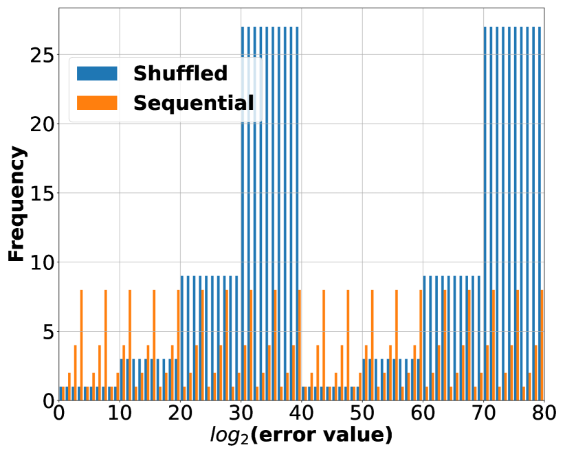
Figure 1(b) shows how shuffling affects the distribution and the count of code error values of the MUSE(80,69) code. The code error values are computed for the sequential (orange bars) and shuffled (blue bars) bit assignments and shown in the histogram. The error values for the sequential bit assignment are fewer, and their frequency distribution per bin is not uniform. On the other hand, with shuffling there are more error values, and their frequency is more uniformly distributed in each bin. However, as expected, the total number of errors with shuffling is much higher than without (the area under the blue bars vs. the area under the orange bars).
Construction The hardware implementation for shuffling is trivial as it requires only minor changes in signal routing between the DRAM interface IO and the memory controller IO. On writes, we encode the codeword, shuffle, and store it to DRAM. When reading the codeword back from memory, we first un-shuffle it and then decode.
III-C Asymmetrical Errors
Here we consider an asymmetrical error model where only one type of erroneous transition is possible: 01 or 10, but not both[49, 60]. Where is this model useful? Using this error correction model is often useful to protect against data retention errors in DRAM to reduce the power spent on refresh. Prior research has shown that the majority of DRAM cells can hold the data longer than the refresh period since DRAM refresh frequency is set to ensure the reliability of the unreliable minority of memory cells[76, 53]. This conservative approach to DRAM refresh increases the power spent to refresh the data and, inadvertently, thwarts performance because during the refresh the memory is unavailable to serve CPU requests. If we had ECC schemes with high reliability guarantees against those types of errors, they might have saved power spent on data refresh and improve power and performance.
To illustrate how MUSE can handle asymmetric errors, without loss of generality, we assume 10 errors only. Thus, the single-bit error value must be a negative integer. Similar to symbol errors, the error values of asymmetrical symbol errors are a combination of negative error values of individual bit flips within the symbol. Using only the negative half of error values cuts down the number of required remainders by half, increasing the chances of finding a one-to-one mapping between errors and remainders.
III-D Multiplier Search Procedure
Algorithm 1 is a pseudocode implementation for finding code multipliers222See Appendix A to obtain the C++ implementation.. The algorithm inputs are the code length , the symbol size , and redundancy . The output is the list of multipliers (empty, if none are found) satisfying the code constraints, i.e., codeword size, symbol size, etc. We denote a satisfying code as MUSE(n,k).
The procedure starts (line 1) by assigning codeword bits to symbols, initializing an empty set of valid multipliers (line 1), and precomputing a required number of remainders for the code (line 1). For every multiplier m (line 1), we compute remainders for error values in the codeword. For each error pattern (line 1) in symbol (line 1), we compute its error values (line 1) by calling (lines 1- 1). An empty (line 1) remainder set is filled with computed remainders (line 1) of each . We compare remainders’ set size to the required number of remainders (line 1); if they match, and all the remainders are not zero, we put multiplier m into the list of valid code multipliers (line 1). We repeat this procedure until we exhaustively checked all multipliers in the redundancy bits .
IV Practical Code Examples
In this section, we describe MUSE codes for different error and system models to showcase the flexibility and applicability of our code in practical modern contexts. Code parameters, i.e., multipliers and shuffles, are summarized in Table I. We denote by a code that encodes -bit of data into -bit codeword. While both Reed-Solomon and MUSE can be designed to handle multiple errors, in this section, we focus only on single-symbol correcting codes as those are often used to guarantee ChipKill in commercial systems.
To help classify the codes, we propose the following naming convention based on the error type covered by code: , where is the error constraint form, is the size of the error, and is error type. We support two types of errors: —bidirectional, i.e., bit flips in both directions, and — asymmetrical, i.e., bit flips in one direction only, i.e., retention errors in DRAM. Both types of -bit errors may be either -bit constrained—marked by , or unconstrained, i.e., any consecutive -bit pattern, marked by . For example, code covers any 4-bit bidirectional error in the codeword, where each -bit error may start at bit , bit , etc., while is a -bit errors that may start at any bit position.
This naming approach highlights the flexibility of MUSE design. For instance, MUSE() covers constrained -bit asymmetrical errors and any -bit bidirectional error. In this case, we would name this code .
MUSE(144,132) Single Symbol Correct (SSC) Code Server and enterprise machines often require a specific capability known as “ChipKill”. Informally, ChipKill allows operation even when one or more DRAM chips on a DIMM completely fail. While the DDR5 standard has been finalized[41] and devices are being sold, older DDR4 devices will likely continue to be utilized for at least a few more years. Hence, we show how MUSE can be used to provide ECC for DDR4 DIMMs. Rather than designing for device failures, we design for handling symbol failures, as symbols are at least as large as DRAM devices and usually a multiple of the device size. Thus, SSC code guarantees to correct errors originating in a single device on a DIMM.
To correct single device failure with x4 devices, we use the MUSE(144,132) code with multiplier and 4-bit symbols. In our scheme, the data bits are striped across two DIMMs with 18 x4 devices each, forming a 144-bit channel333Those 144-bit channels are quite common in systems with IBM Power9[31] and Intel Xeon[2] CPUs. Under these conditions, MUSE ECC uses only 12 check bits for 132 bits of data444We use the term “data” to refer to amount of useful information in the codeword, and not to the native data sizes.. In contrast, a traditional Reed-Solomon code will use 16 check bits for 128 bits of data.
MUSE(80,69) SSC Code The recently published DDR5 standard[41] doubles the number of channels per DIMM, requiring two 40-bit memory channels per DIMM (32-bit data + 8-bit parity)[66]. As of this writing, there are no commercially available DDR5 ECC DIMMs, and as such it is not clear how exactly the DIMMs will be configured. It is possible that they could be made of ten x4 devices per channel, for a total of 20 devices per DIMM, or five x8 devices per channel, for a total of ten devices per DIMM.
Like in DDR4, we propose a 4-bit symbol (80,69) code with data striped across two channels. MUSE(80,69) code encodes 69-bit data into 80-bit codewords, using only 11 redundancy bits. With this code, by using only 64-bits for data, we can correct failure of one device on a DIMM with five bits to spare; or we can recover two consecutive device-failures with one bit to spare. In contrast, a traditional Reed-Solomon(80,64) code with x8 symbols has no spare bits.
MUSE(80,67) Single Device Correct Code Suppose that we wish to correct a single device failure, and we do not wish to draw data from two channels on a DDR5 DIMM. Even in this case, we can design a MUSE code. Assuming asymmetrical errors, we can design a code with 8-bit symbols for DDR5 DIMMs. For this code, sequential assignment of bits to symbols yields no multipliers of 16-bits or less. Thus, we shuffle the bits between symbols. As a result we found a multiplier for the following shuffle:
| (5) |
This MUSE(80,67) code encodes 64 bits of data and three bits of metadata into an 80-bit codeword while correcting a single device failure. To use this code over a 40-bit channel with 80-bit codewords, we split the codewords such that every bus transaction carries half of the 8-bit symbol to memory (for all symbols). A similar approach is used by AMD[4].
MUSE(80,70) Single Device Correct Hybrid Code To showcase the flexibility of the construction approach, we design a 4-bit symbol code that handles two classes of errors: (1) asymmetrical symbol errors, and (2) bidirectional single-bit errors. We call codes that correct more than one type of error Hybrid codes. As a result, the code encodes 64-bit data and 6-bit metadata into 80-bit codewords and corrects two classes of errors. Code parameters are with the following shuffle:
| (6) |
V MUSE Microarchitecture
In this section, we discuss the microarchitectural implementation of MUSE codes. We start with the system-level integration, discuss the design of the encoder and decoder, and conclude with lower-level building blocks and optimizations for fast multiplication and fast modulo operations that are required to build efficient decoders and encoders.
V-A System Overview
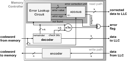
Figure 2 shows a high-level overview of MUSE integrated into a system. On the read path, for every word read from the main memory, the decoder computes the remainder, which is passed to the Error Lookup Circuit (ELC) to determine whether an error has occurred. If the ELC provides a value to correct the data, then error correction is performed, and the Last Level Cache (LLC) will read the corrected data. On the write path, the data are read from the LLC, encoded, and transmitted to the memory.
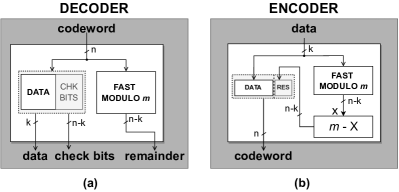
Decoder Figure 3(a) shows the microarchitecture of the decoder. The decoder uses a fast modulo (described in Section V-B) circuit to compute the remainder, which is used for error detection and correction. The decoder is systematic, i.e., utilizes the separability of the data and does not require division like in non-systematic residue codes.
Encoder The encoder in Figure 3(b) is similar to the decoder as it computes the residue using fast modulo. However, unlike the decoder, encoders need to calculate the value of X (see Eq. 4) to ensure that .
Error Correction Figure 2 shows the implementation of the error correction unit which consists of the Error Lookup Circuit (ELC) and an adder. Each entry in the ELC contains a remainder, error value, and the sign bit for the adder. The remainder from the decoder’s output is compared against the remainder field in the ELC entry, and upon a match, the error value is used to correct the error. The sign bit in the matched entry directs the adder to subtract or add the error value to the codeword. For example, for MUSE(144,132) code with , the error correction is built around ELC with 1080 entries and an adder. Each entry is 157 bits wide, where the first 12 bits are the remainder value, the next 144 bits are the error value, and the remaining bit is the adder sign bit.
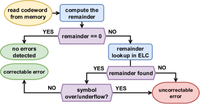
Error Detection There are two ways to detect multi-symbol errors with MUSE: (1) the computed remainder is not present in the ELC, or (2) symbol-overflow/-underflow during error correction (as shown in Figure 4). The first method utilizes the fact that the code multiplier is greater than the number of remainders it generates, leading to some remainder values being unused. Hence, if the ELC does not find the matching remainder entry, it declares an uncorrectable multi-symbol error. We base the second detection method on the observation that errors are symbol-confined by design. Thus, if some miscorrected multi-symbol errors cause flipping bits beyond the boundary of the corrected symbol, the multi-symbol error is detected. This method works because the errors are corrected with addition/subtraction, and in the case of a multi-symbol error, it may cause a ripple of 1s or 0s beyond the symbol boundary.
V-B Fast Arithmetic Blocks
| Process | Operations | ||
|---|---|---|---|
| decode |
|
||
| \cdashline1-2[1pt/1pt] encode |
|
||
| are the redundancy bits, or | |||
We build MUSE with three arithmetic operations: integer division, multiplication, and modulo. Both encoding and the decoding are done by computing the modulo (see Table II).
Division by Constant The decoder uses modulo for error detection/correction and relies on a fast dividers and multipliers. However, even the fastest processors take 13–95 cycles for integer division [24]. Two insights help us to substantially reduce decoder latencies: (1) a general divider is not required since we always divide by a known multiplier of the code m. (2) using multiplication by the inverse instead of the division—a known optimization technique in compilers [28, 51, 7]. As a result, we reduce the problem of designing a fast divider to a task of designing a fast multiplier by a constant.
Multiplication by Constant Generic integer multiplication of 64-bit operands is typically done in 3–4 cycles in most modern CPUs. However, because decoding is on a critical path and the codewords are at least 80-bit long, we need a much faster multiplier. We achieve this goal with a custom Wallace Tree[75] multiplier based on Radix-4 Booth Encoders[55]. Figure 5(a) outlines the multiplier with its three components: (1) Multiplier encoder with Radix-4 Booth Encoding (BE), which reduces the number of partial products by half, and makes the tree shallower, (2) Wallace tree that performs the summation of partial products, and (3) a final adder that produces the result. We optimized the depth of the Wallace Tree further by analyzing partial products and removing those always equal to zero from the multiplier tree, further reducing the latency, hardware, and energy costs of the multiplier. For example, for the MUSE(144,132) code, Booth Encoding of the multiplier’s inverse value has 73 partial products, of which 23 are equal to 0. By eliminating these, we reduce the depth of the Wallace tree by one level, thus reducing the latency by three XOR delays. Table III summarizes the multipliers, their inverses and shift amounts we used to implement the codes.
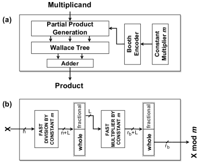
| m | Inverse Value |
|---|---|
| 1761878725188230243585305α | |
| 753922070210341214920295β | |
| shift right by: 156, 87, 93, and 89 bits | |
Modulo by Constant The naive approach to compute mod m is as follows:
| (7) |
where the division may be a multiplication with the inverse. As a result, the latency of the modulo operation is the latency of two multiplications and one subtraction, which can be done in 7 cycles on a modern CPU[24]. However, the technique developed by Lemire et al. [51] allows computing the modulo even faster. The idea is based on using discarded fractional bits from the division (within in Eq.7). When the value represented by these bits is multiplied by the code multiplier m, the upper bits of the product are equal to the result of a modulo. Figure 5(b) shows a schematic of a circuit implementing this scheme with two consecutive multiplications. The second multiplier is much faster than the first one because it multiplies by m – a much smaller integer than the inverse of m. Therefore, the resulting latency of a custom modulo circuit is much shorter than the latency of serialized CPU operations.
VI MUSE Use Cases
In this section, we discuss co-design opportunities for MUSE codes.
VI-A Exploiting Unused States for Security
Let us start with an obvious case. Consider a MUSE(80,69) code with an -bit multiplier , thus giving us five bits of space that one can use for metadata. In other words, with an 80-bit codeword, we can store up to 69 bits of data and still get ChipKill-like functionality, but since the basic granule of protection is 64 bits (8 bytes) in most existing schemes, we get to store five additional bits of free storage. This storage can be put to several uses, for example, the ARM Memory Tagging Extensions (MTE)[3] or Rowhammer detection[48]. We discuss the integration of MUSE with ARM MTE in Section VII-D, and in the next section we discuss Rowhammer resiliency.
Rowhammer Detection In 2019, Cojocar et al. [18] showed that it is possible to bypass the ECC and execute a successful rowhammer-based attack on a system. Indeed, common ECC schemes are not designed to withstand a high number of bit flips within a codeword as their detection capabilities are limited by available ECC storage. Because MUSE is more storage-efficient, it can be used to mitigate Rowhammer-based attacks (e.g., [80]). For example, we use the salvaged five bits per word provided by MUSE(80,69)— which amounts to 40 bits per cache line—to store a hash code of the cache line’s worth of data. Hence, when the attacker rowhammers the bits in memory, they must also predictably corrupt the hash; otherwise, the attack will be detected due to the hash mismatch. Thus, the attacker must profile the effectiveness of Rowhammer on a cache line and not a word granularity, as they have to be sure that the corrupted cache line and hash match. If the attacker misses flipping one of the bits, the attack will fail with the probability of (i.e., the chance of collision for a 40-bit hash). In addition, the attacker should consider that presence of even a simple ECC scheme increases the time to rowhammer from minutes to days[18]; with hashing, the time to carry out the attack may increase to weeks, rendering this kind of exploitation impractical.
VI-B Reliable Processing In-Memory
The idea behind Processing In-Memory (PIM) is to compute near the data—i.e., in the main memory. Recently, PIM advanced from a theoretical research topic toward a practical hardware implementation of the multiply-accumulate (MAC) units within a commercial-grade HBM2 device[50]. While the parity-based ECC seems to be a natural choice to protect the data of PIM modules, MUSE is more advantageous because it can protect both the stored data and the computation itself without the need to convert the redundancy information between the codes. For example, let us consider a setup used by Lee et al. [50]: an HBM2 device with integrated MACs for the acceleration of neural-network applications. In this device, the data are read in 256b words and transferred to MACs for computation. To protect the data and the compute, one can use MUSE() code with only 12 bits of redundancy. HBM provisions 64b for ECC storage for each 64B of data, or 32b per 256b of data – more than needed for MUSE() code. The saved 20 bits from multiple 256b words provide enough space to store cryptographic authentication codes to guarantee the integrity of the data. Moreover, PIMs may use error information to diagnose the arithmetical units at runtime and guarantee reliable computation.
VII Results
In this section, we study the following research questions:
-
1.
How do MUSE and Reed-Solomon code trade off storage for higher reliability guarantees?
-
2.
How do the VLSI overheads of MUSE compare to traditional codes?
-
3.
How does the performance overhead of MUSE compare to Reed-Solomon codes?
-
4.
What are the benefits of co-designing MUSE with memory tagging?
-
5.
How does the flexibility of MUSE compare to a Reed-Solomon code?
VII-A Reliability Trade Off: Reed-Solomon vs. MUSE
To compare Reed-Solomon and MUSE codes, we evaluate them across four parameters: (1) number of saved bits, (2) practicality for DRAM, (3) single symbol error correction, and (4) multi-symbol error detection rates.
Saved Bits, Practicality, and Error Correction Both Reed-Solomon and MUSE ECC can be designed to offer space to store the metadata. Reed-Solomon codes that offer saved bits, however, are not practical in the context of DRAM memories because they may store more than one symbol in a single chip. For example, let us assume a DIMM made with 4-bit DRAM devices protected by Reed-Solomon code with 5-bit symbols. This code saves six bits of storage, permitting 134 bits of data to be encoded into a 144-bit codeword. In this scenario, the last bit of the first symbol and the first three bits of the second are written to the same x4 device. If that device fails, the code will not correct the error because there are two corrupted symbols instead of one. Thus, this Reed-Solomon code cannot offer ChipKill error correcion. Hence, we always need to evaluate bits savings in the context of the resulting code.
Error Detection MUSE ECC allows repurposing saved storage to gain higher multi-symbol error detection rates. This can be done by choosing a larger multiplier value that can be stored within the available redundancy bits. For example, we can design two codes: MUSE(144,128) and MUSE(144,132). While both codes offer single symbol correction, the first code gives up four saved bits to store a larger multiplier value ( vs. ) and gains higher multi-symbol error detection: 99.17% vs. 86.71%. The Reed-Solomon code, on the other hand, trades off both error correction and detection guarantees to gain storage, effectively rendering those codes impractical. However, while choosing zero saved bits, both RS(144,128) and MUSE(144,128) offer similar multi-symbol detection (MSED) rates of 99.36% and 99.17%. If the saved bits are used store a hash, as they are used in Rowhammer protection, MUSE’s MSED rate increases even further to the chance of detectable hash collisions, which is likely higher than the MSED rate achievable by a Reed-Solomon code, while achieving better security.
Table IV shows MSED rates and bit-savings for various Reed-Solomon and MUSE codes constrained to 144-bit codeword for x4 (5-bits savings shows MUSE(80,69) code). We see that both code families provide spare bits at the cost of reduced multi-symbol error detection rates. However, Reed-Solomon codes also lose ChipKill guarantees due to misalignment of symbols with device boundaries because of the constant two-symbol redundancy. For instance, to gain four spare bits with Reed-Solomon codes, one must use 6-bit symbols (12-bit redundancy) to design RS(144,132) code. This code is not practical because 6-bit-wide DRAMs do not exist. On the other hand, with MUSE ECC, one simply picks a multiplier that guarantees ChipKill correction and the desired bit savings. Moreover, due to their construction constraints, Reed-Solomon codes offer bit savings only in multiples of two, while MUSE allows for more fine-grained trade offs between the required storage and MSED rates.
To compute multi-symbol detection rates, we used a Monte-Carlo-based simulator. In an -symbol codeword, the simulator randomly samples 10000 out of all possible -symbol error patterns. Each of the chosen symbols is randomly corrupted, constructing a multi-symbol error. For each multi-symbol error, we computed a syndrome and compared this syndrome to all the syndromes of single symbol errors. If no match is found, then that specific multi-symbol error is detectable. Additionally, MUSE also detects multi-symbol errors caused by the ripple of 1s or 0s across symbol boundaries. The fraction of detectable multi-symbol errors, out of all sampled multi-symbol errors, is the multi-symbol error detection rate.
Bit savings and Multi-Symbol Error Detection rates.
Code Extra Bits 0 1 2 3 4 5 6 RS 99.36 Ø 95.55 Ø 86.79 Ø 53.96 MUSE 99.17 98.35 96.70 93.39 86.71 85.03 Ø Legend: Ø Code does not exist. 144b ChipKill protection. 80b ChipKill protection. Not practical code – does not guarantee ChipKill protection. MSED Error detection across multiple DRAMs at the same time.
VII-B VLSI Overheads
Code Encoder Error Corr. & Det. GEM5 Latency Latency, ns std_cells Area, Power, Latency, ns std_cells Area, Power, Enc Dec MUSE(144,132) 1.129 33312 10999 5.11 1.048 45493 13648 8.56 3 0 MUSE(80,69) 1.177 11953 4166 5.22 1.179 18422 5593 5.64 3 0 MUSE(80,67) 1.154 14655 4896 4.14 1.018 24043 7092 6.22 3 0 MUSE(80,70) H 1.181 13775 4772 4.15 0.859 18937 5719 5.80 3 0 RS(144,128) 0.219 1158 737 2.67 0.376 2884 1053 2.70 1 0 RS(80,64) 0.124 542 359 1.31 0.381 2540 617 1.99 1 0
We implemented the basic arithmetic blocks, decoders, encoders and error correctors in Verilog and synthesized them with Synopsys Design Compiler Version: R-2020.09-SP4 using NangateOpenCell 15nm open-source standard cell library[57]. The synthesis ran with hierarchy ungrouping and high effort for delay, power, area optimizations. Table V summarizes the latency and silicon area for the components of all discussed codes.
The encoder latency of the MUSE(144,132) code is 1.129ns, while the error correction latency (including remainder computation and ELC) is 1.048ns. Assuming a clock frequency of 2400 MHz (or 417ps), the encoder delays the writes to the main memory by three clock cycles, while error correction delays the reads by three clock cycles. For the systematic code, in the common case of no errors, reads have no delay.
Reed-Solomon Code Implementation We picked Reed-Solomon codes because they are representative single-device correct ECC schemes. The Reed-Solomon code is systematic; thus, no decoding is required. We picked the PGZ algorithm[77] to implement the encoders and error correction units for Reed-Solomon codes. In addition, for simplicity, we picked lookup tables to implement Galois Field arithmetic.
Reed-Solomon encoders are simple XOR trees implementing binary multiplication of generator matrix and data, resulting in low area overheads and single clock cycle latency. However, error correction is more complicated as it requires Galois Field arithmetic. Hence, the main factor differentiating Reed-Solomon codes’ latency and silicon area of the error correction circuitry is the symbol size, i.e., the number of entries in the lookup tables for symbol arithmetic. The latency for error correction is 0.38ns, area overheads are between 842 to 1053, and power consumption ranges from 2 to 2.7mW (See Table V).
Comparison Because the Reed-Solomon codes can be implemented with simple XOR trees of moderate depth, they result in a smaller area and shorter latencies than comparable MUSE codes. For example, MUSE(80,67) code uses more silicon area than RS(80,64), adding two more clock cycles of latency. These high area overheads are expected because Wallace Tree nodes are two serially connected full adders, while XOR trees use a single XOR gate. For the error correction, Reed-Solomon has a slightly smaller delay of single a clock cycle vs. three cycles of MUSE. The lead of Reed-Solomon codes is not surprising, as those are natively suited for binary arithmetic.
VII-C Performance
Simulation Setup We evaluated the performance impact of MUSE ECC with the gem5 simulator [9] and SPEC 2017 (v1.1.5) benchmarking suite[12]. We configured a Haswell-like CPU with 3.4GHz frequency, 64kB L1 cache equally split for instructions and data, L2 256kB/core, L3 of 8MB, and 32GB DDR4 memory. For the simulation, we picked the TimingSimpleCPU model that provides a detailed timing simulation of the memory subsystem while executing instructions in a single clock cycle. We used gcc 4.8.5 to build dynamically-linked fprate and intrate SPEC 2017 benchmarks with -O3 optimization level. We executed the benchmarks with the reference inputs for 10 billion instructions, which is long enough to warm up the caches and put the system in a steady state.
To emulate encoding latency, we delay each write transaction on the memory interface by the latency of the encoder. There is no decoding penalty because all the evaluated codes are systematic. To estimate performance penalty due to the delay of error correction, we delay memory reads by the latency of the error-correcting circuit. To achieve this goal, we modified the memory controller of the gem5 simulator. For convenience, the extra latencies are summarized in the last two columns of Table V.
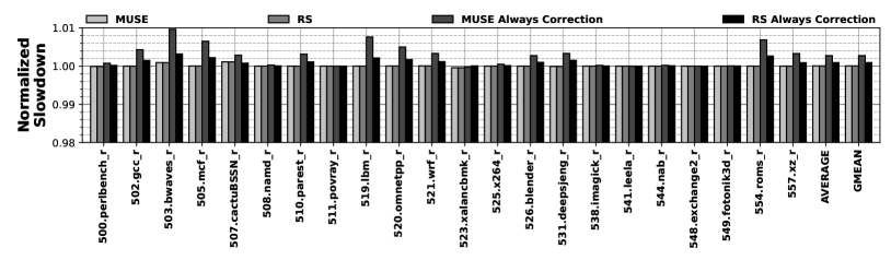
Results and Discussion Figure 6 summarizes the slowdown of SPEC 2017 due to two evaluated scenarios: (1) error-free operation, and (2) error correction on every read operation. We see from the figure that MUSE (blue bars) and Reed-Solomon (orange bars) have similar performance to the baseline, despite MUSE taking two more cycles for encoding than Reed-Solomon. This is likely as write operations are rarely on a critical path of the system, and delaying them by one or three cycles is unlikely to be critical for performance. In the worst-case scenario where every memory read results in corrupted data, Reed-Solomon (red bars) would have a slightly better performance than MUSE (green bars)—a slowdown of 0.09% vs. 0.2% on average. As we see from those results, performance overheads of MUSE are minimal and comparable to those of the Reed-Solomon code.
VII-D Case Study: Memory Tagging
In this section, we analyze how the use of MUSE with ARM MTE[3]-like memory tagging security scheme improves the power consumption of a system without impact on performance. As a baseline, we assume a system with ECC and a memory tagging scheme where every sixteen bytes of memory have a four-bit tag (similar to ARM MTE), i.e., 16 bits of metadata for 512 bits of data.
Overview There are two approaches to implementing this scheme in hardware. In the first approach, the metadata is stored in a disjoint manner in a special region of the main memory. Thus, when the metadata is needed, an additional memory request would bring it to the CPU from the main memory. To mitigate the penalty of additional memory reads on performance, metadata caches may be used to cache the metadata for later use, effectively reducing the number of memory reads. The downsides of this approach are (1) more complicated design (integration of metadata caches, additional state machines to track the metadata state, etc.), and (2) increased power consumption due to metadata memory traffic and metadata caches. The second approach is to store the metadata in the ECC portion of the main memory, forgoing all ECC guarantees of a system. The benefits of this approach are clear: (1) in-lined metadata, (2) no need for more complex hardware, and (3) no increased power consumption as only the relevant metadata is fetched from DRAM. The downside is that the system has no ECC. MUSE allows the system designer to enjoy the benefits of both approaches by storing the in-lined metadata in the unused bits of the code to gain performance, lower power consumption, simplify the design, and keep ChipKill-level ECC protection.
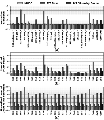
Evaluation Setup We evaluate the following aspects of the system: (1) performance, (2) memory bus traffic, and (3) power consumption. To do so, we modified the gem5 simulator to issue an additional memory read for each cache miss to read a cache line worth of metadata from reserved memory space. In addition, for the system with metadata caching, we introduced a 32-entry 16kB metadata cache for memory tags. We conservatively assume that metadata caches consume no power. We used the same gem5 configuration as in Section VII-C and evaluated the following three configurations: (1) memory tagging with MUSE, (2) Reed-Solomon ECC with, and (3) without metadata caches. The SPEC-2017 benchmarks were run for 10B instructions on each of those configurations to measure execution latency, DRAM power consumption, and the number of read/write transactions on the memory bus.
Results and discussion We summarize the simulation results in Figure 7. Figure 7(a) shows that only the introduction of the metadata caches can eliminate the overheads of memory tagging and equalize its performance with that of MUSE—an improvement of about 1% compared to metadata-less memory tagging. Moreover, while the metadata caching reduces DRAM power consumption from 1.7% to 0.72% (peaking at 2.8% for 519.lbm), MUSE still saves on average 0.72% of DRAM power (Figure 7(b)). Finally, Figure 7(c) shows that while the metadata memory requests improved with caching (67% vs. 12% on average), memory tagging with caches still requires, on average, 12% more metadata accesses than MUSE, which requires zero additional memory requests due to its storage efficiency. These metadata requests will result in the increased power consumption of the CPU’s memory controllers.
Table VI summarizes the total power consumption of the evaluated schemes. As we see from the summary, despite requiring more silicon area and power for MUSE, the overall system with memory tagging and MUSE saves at least mW and 12% of memory bandwidth while offering ChipKill guarantees and a simpler system design.
Scheme Components, [mW] DRAM ECC Total [mW] diff, [mW] MT w/ MUSE 6468 6496 0 MT w/ 16kB cache 6517 6527 MT w/o cache 6601 6611
VII-E Flexibility: Reed-Solomon vs. MUSE
Here we evaluate the flexibility of Reed-Solomon and MUSE codes by comparing how the code length, symbol size, and redundancy are interlinked and their effect on the properties of a resulting code. We define the code as flexible if its codeword and data length can be adjusted with fine resolution (e.g., single-bit), the code can accommodate different symbol sizes multiple error models efficiently.
For the Reed-Solomon code, redundancy, code, and data lengths are all functions of the symbol size. For example, for a single-symbol error correcting Reed-Solomon code, the redundancy is always two symbols long. Hence, there is only one Reed-Solomon code for a given symbol size and codeword length. Moreover, the Reed-Solomon code by design does not differentiate between bit flip directions, making it a poor fit for the model of asymmetrical errors, as the Reed-Solomon code will require the same number of redundancy bits for asymmetrical and bidirectional errors.
For MUSE ECC, symbol size and code length define the set of valid code multipliers—basically determining the number of redundancy and data bits in the codeword. If the number of available data bits is more than needed, i.e., the code works with fewer redundancy bits, these saved bits can store the metadata, be used for larger multiplier values improving error detection, or can be discarded to create a shorter code (saving system resources). In addition, MUSE ECC allows the combination of multiple physical error models into one code as long as a suitable multiplier is found.
VIII Related Work
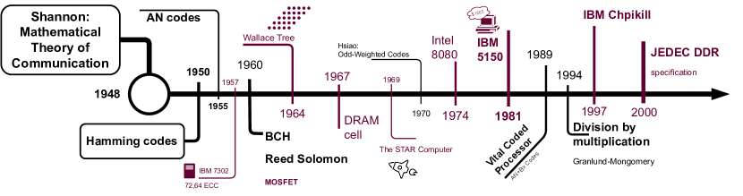
MUSE builds upon an interesting 60-year history of prior work on error correction (a brief historical overview is shown in Figure 8).
Around the same time when BCH and Reed-Solomon codes were developed[32, 10, 65], in 1960 Brown published what is now referred to as an “AN” code[11]. The work was developed in the context of robust error correction for arithmetic circuits. To generate a codeword for a data, a word it is multiplied by an integer . To retrieve the data word (and/or check for errors), the code word is divided by . In AN codes, if the sum of two codewords, say, and , is also a code word, , then any error in addition or subtraction can be identified by dividing the result by and checking the error remainder. A variation of AN codes called residue codes [30, 16] were also developed in the context of fault-tolerant arithmetic units. Instead of creating a code word as , residue codes are created as , where is a power of 2 and is the remainder when is divided by a multiplier . The nice thing about this construction is that it makes the code systematic, i.e., the data bits are separated from the check bits. This work and other works[56, 8] were published in the pre-Moore’s-Law era, when there was a significant paucity of transistors and when multiplications and divisions were too expensive to check addition[34, 54]. These ideas appear to have remained of theoretical interest till the early 70s[6]. In 1970, The STAR Computer[5]—a research project funded by NASA to develop a reliable computer for space probes[20]—used residue codes. Since then, residue codes continue to be used to guarantee the reliability of arithmetic units in the CPU (e.g., [63]). In 2010, Sullivan [72] systematically evaluated the overheads of residue checking for various error models in the context of modern ALUs.
In 1967, Dennard invented DRAM[22], and soon after there was a flurry of work on improving the reliability of these new “high-speed” memories[13]. While technology scaling in the 1970s permitted the creation of single-chip microprocessors in this era, latency was still a significant concern, and it was believed that high-speed memories would need error correction techniques that can “encode and decode” in parallel[64]. Alas, the arithmetic and residue error codes cannot be parallelized unless significant restrictions are placed on the multiplier. In 1970, Hsiao published his seminal work on Odd-parity weight codes[33] that balanced the delay of the syndrome calculation for a SEC-DED code using only seven levels of fast XOR gates. Thus, the idea of AN and residue codes was put aside again.
In the 1990s, with companies like Rambus, DRAM became even faster due to innovative signaling techniques, which cemented the place for lightweight Hsiao-like codes; since then, these constructions have remained the de facto standard for many systems. Effectively by this time, the value of AN and residue codes appear to have disappeared from the collective memory of the research community as evidenced by the lack of papers on this topic. At the same time, in a completely different community, a technique that is key to unlocking the potential of these codes was being developed.
In 1994, Granlund and Montgomery published a paper “Division by invariant integers using multiplication”[28] at the PLDI Conference. They observed that computers were multiplying much faster than dividing—around one order of magnitude—so they asked the question: would it be possible to perform a division as a multiplication? For division by constants, this is clearly possible, especially if the constants can be pre-computed at the compile time of the program. For instance, to divide a number by , we can multiply it by . To avoid the floating-point multiplication, we first multiply the inverse of by a large integer power-of-two and then divide the result by the same integer power-of-two. We replace the last division with a very cheap shift operation. We leverage this advance to make MUSE hardware very fast.
In the early 90s, most server systems still employed parity for error detection. The race for more reliability and availability features increased with the rise of e-commerce websites in the late 90s. IBM introduced “ChipKill” memory[21, 39], a commercial name for a system that continues operation even if an entire DRAM device fails. Basically, in the late 90s, the error model moved from single errors to supporting burst errors. These availability features were also used in space missions, such as NASA’s pathfinder MARS probe[39]. In contrast to these popular burst codes, MUSE provides the same reliability with fewer check bits.
In 2000, JEDEC standardized the DDR interface to memory[40]. Standardization meant interoperability, but it also introduced several constraints on how memory would be integrated, and, pertinently, how error correction could/should be performed. DDR4 memory ECC DIMMs are 72-bit wide: 64-bit data and 8-bit check bits. This architecture can be used to implement a (72,64) code, or a (144,128) code[4]. Typically, the (72,64) code supports SEC-DED using Hsiao or Hamming codes, and (144,128) is used for single and burst error correction. With the continuing technology and voltage scaling trends, DRAM has suffered more and more reliability problems, especially Low-Power DDR memories (used in mobile phones and embedded devices). As mitigation, vendors started to implement on-die ECC[62, 38], typically as simple single error correcting codes without the ability to correct burst-errors. The idea of using on-die error correction has now been standardized in the latest generation of JEDEC’s DDR5 standards[41].
For the modern servers and mainframes, the reliability requirements are more demanding. For example, AMD[25, 4], IBM[31], and Intel[2, 1] systems offer ChipKill-level guarantees for DIMMs with x4 and x8 devices. Due to ECC construction constraints, standard x8 DIMMs do not have enough DRAM chips to offer ChipKill over a single 72b channel. To mitigate this, IBM manufactures custom DIMMs with x8 DRAMs, uses 144-bit busses between the memory controller and the DIMMs, and makes cache lines 128-byte long in the POWER9 series CPUs[36, 31]. With these techniques in place, IBM systems support at least a single device failure. For x4-based DIMMs and custom x8 DIMMs, some IBM systems may tolerate two consecutive device failures on a pair of DIMMs[31]. Similar guarantees are provided by Intel for x4-based DIMMs with its Double Device Data Correction (DDDC) scheme[1, 2]. However, because Intel systems are mostly based on off-the-shelf components, DDDC does not support x8 DIMMs. While MUSE’s support for x8 DIMMs is to be developed, we offer protection against two consecutive device failures for x4 DIMMs, and, unlike commercial solutions, our code has the ability to be tuned for a specific error model.
Academic ECC schemes tend to be more diverse than current commercial solutions. These proposals range from a new codeword organizations (e.g., [45, 43]), ECC enablement in systems without ECC (e.g., hashing and checkpointing[15], virtualization of ECC[82], memory compression for ECC[46]), extension of ECC to both DRAM data and control signals[47], use of small caches within the DRAM[70, 14] to multi-tier and/or concatenated codes (e.g., [27, 74, 81]). More recent academic ECCs design considering the on-die ECC of modern DRAMs. For example, XED[61] and PAIR[42] work in conjunction with on-die ECC, while DUO[26] repurposes on-die ECC’s storage to increase the number of bits for redundancy of the memory controller’s ECC, thus increasing the strength of the resulting scheme. Those, and many other solutions, consider ECC only for its main purpose—to achieve reliable, error-free system operation. MUSE, on the other hand, optimizes for two objectives at the same time: ChipKill-level error correction and availability of in-lined metadata. Nonetheless, on-die ECC is an integral part of the new DDR5 DRAM[41], and, thus, we believe that the investigation of MUSE co-design with on-die ECC is an interesting topic for future work.
However, ECC may improve not only the reliability but also the power consumption of a system. For instance, [17, 58] use strong ECC schemes to enable reliable operation of caches in near-threshold regime, saving 34 to 71% of system power. However, these power savings come at the cost of trading off a significant portion of the cache to store ECC bits (up to 50%), which may be an acceptable trade-off for a system in a low-power mode. In contrast, we designed MUSE to minimize the memory footprint of the ECC to improve system performance, power efficiency, and memory bandwidth utilization. Due to MUSE’s storage efficiency, it may be a perfect candidate for caches operating in near-threshold regimes, but a detailed cost-benefit analysis requires a detailed study which we leave for future work.
Along with the growth in reliability problems, the last decade also witnessed an increase in security problems. Several recent security solutions increase the demand for memory, including memory encryption[44], adding authentication code[19, 52], or requiring additional storage to support software security (e.g., [3, 37, 68, 79]). We developed MUSE to support both error correction and security. Prior works in the area of co-designing security and reliability assume standard ChipKill or SEC-DED codes[35, 29, 69, 73, 67], and those codes do not provide a way to extract more states for security or performance features or reduce the amount of storage for reliability which are key contributions of MUSE.
IX Conclusion
In this paper, we present MUSE—a novel ECC construction that provides a ChipKill-level of error correction but crucially also allows spare ECC space to be harvested and used for additional purposes. To make MUSE work in modern settings, we revisit old formulations of residue codes and extend them with two novel optimizations—symbol errors and shuffling of bits. With these optimizations, we show that MUSE can act as a “drop-in” replacement for commonly used ChipKill ECC schemes while using fewer bits for storage. Moreover, when we evaluated MUSE ECC in ensemble with security technique of Memory Tagging, we found out that the system is more power efficient than system with conventional Reed-Solomon codes. The benefits of MUSE codes also go beyond space savings and holding metadata. For instance, MUSE codes integrate much more easily into Processing In-Memory devices, making MUSE a very exciting ECC option for the next decade and beyond.
Acknowledgment
This work was partially supported by Qualcomm Innovation Fellowship. Any opinions, findings, conclusions and recommendations expressed in this material are those of the authors. Simha Sethumadhavan has a significant financial interest in Chip Scan Inc.
Appendix A Artifact Appendix
A-A Abstract
This artifact contains the following three components
-
1.
Multiplier Search: the implementation of the code search procedure outlined in Algorithm 1 in the paper.
- 2.
-
3.
VLSI implementation: Verilog implementation of MUSE and Reed-Solomon codes used in the paper.
Artifacts (1) and (2) are provided in the form of the Docker container, so they are easy to set up and run. Artifact (3), however, has only the Verilog code as we used proprietary tools we cannot share. However, (3) is easy to reproduce once you have access to the tools as we used a default Synopsys RM-Flow (see Section A-H). Each of the provided artifacts has a detailed README.md file with instructions.
A-B Artifact check-list (meta-information)
-
•
Algorithm: Code search procedure (Algorithm 1 in the paper)
-
•
Compilation: performed automatically within the docker container.
-
•
Run-time environment: Docker container.
-
•
Hardware: x86_64-based system.
-
•
Execution: No requirements.
-
•
Metrics: Valid code multipliers are reported if found, figure pdf files.
-
•
Output: A text file per experiment with search configuration supplied via command line, i.e., codeword and symbol lengths in bits, redundancy budget in bits, etc., and a list of found multipliers. Both figures as pdf files.
-
•
Experiments: Four experiments are required to reproduce the codes reported in Table 1. In addition, the user may change command line arguments to see how those affect code feasibility, i.e., the configuration of MUSE(80,67) code without shuffling finds no multipliers. 280 gem5 simulations.
-
•
How much disk space is required (approximately)?: about 30 GB.
-
•
How much time is needed to prepare workflow (approximately)?: 10-20 minutes to build the containers (depending on the internet connection).
-
•
How much time is needed to complete experiments (approximately)?: Code Search: less than 20 minutes to build the container and run all the experiments (automated via docker image). gem5 simulations require 36 hours on M5zn AWS instance (48 cores).
-
•
Publicly available?: Yes.
-
•
Code licenses (if publicly available)?: APACHE 2.0
-
•
Workflow framework used?: Docker containers.
-
•
Archived (provide DOI)?: https://doi.org/10.5281/zenodo.7019209
A-C Description
A-C1 How to access
The artifact is licensed with Apache 2.0 license and can be downloaded from https://doi.org/10.5281/zenodo.7019209. The artifact contains the source code, installation instructions, and steps to run the experiments.
A-C2 Hardware dependencies
The artifact was developed and tested on x86_64-based system with Intel Core i7-8700 CPU.
A-C3 Software dependencies
For the code search, the artifact requires boost C++ library v1.74 and g++ (v10 or v11) compiler. For the gem5 simulations, SPEC 2017 benchmarking suite is required. For Verilog synthesis, Synopsys Design Compiler, PrimeTime PX tools, and NangateOpenCell 15nm open-source standard cell library are required (those are not included in the artifact, the library can be obtained for free via https://si2.org/open-cell-library).
A-D Installation
Multiplier Search. The code search supports two ways of installation: (1) automated via docker container or (2) manual compilation.
-
•
The preferred way to evaluate the artifact is to use provided docker container: download and install docker daemon via https://docs.docker.com/get-docker/. Build the container in the root folder of the artifact with docker build -t muse:muse .. The docker image both builds the source code and performs the multiplier search.
-
•
Alternatively, install boost library via sudo apt install libboost-all-dev and compile the source code with g++ --std=c++17 -pthread code_search.cpp.
For convenience, the artifact comes with README.md file explaining both of these options.
Simulations with gem5. gem5 simulations are performed in the provided docker container which includes a modified version of the gem5 simulator, which can be built with docker build -t muse-gem5:muse-gem5 . User is required to have their copy of the SPEC 2017 benchmarking suite installed at /all_data/spec2017. Note, that SPEC 2017 installation location is customizable, see included README.md for more details.
A-E Experiment workflow
Multiplier Search. The experiments are performed automatically during the container build process. Multiplier search results can be examined by opening the container interactively: docker run -i -t muse:muse bash.Once the shell is available, four text files with the .result extension contain the set of found code multipliers for each executed search configuration.
To execute the experiments manually, run the compiled binary with configuration matching desired code constraints. For example, to run the search for 144-bit codewords with a 12-bit redundancy budget (i.e., MUSE(144,132) code), use the following command line parameters:
-
•
12-bit multipliers -p 12
-
•
144-bit codewords -b 144
-
•
4-bit symbols -m 4
-
•
(optional) multithreading -t 8
Please refer to the --help output for the remaining command line options of the compiled binary or see the examples in README.md.
Simulations with gem5. The simulations should be launched via make sim. When the simulations are finished, the figures are plotted with make figures. As a result, Figure6.pdf and Figure7.pdf will appear. Please refer to included README.md for more details about the manual line-by-line process.
A-F Evaluation and expected results
Multiplier Search. Four experiments are performed automatically during the installation steps of the artifact for each reported MUSE code in Table 1 in the paper. Each search configuration will result in at least one found multiplier (highlighted values are used for the codes reported in the paper):
-
•
For 144b codewords with 12-bit redundancy, and 4-bit symbols: 2397, 2883, 2967, 3009, 3259, 3295, 3371, 3417, 3431, 3459, 3469, 3505, 3523, 3531, 3551, 3555, 3621, 3679, 3739, 3857, 3909, 3995, 4017, 4043, 4065.
-
•
For 80b codewords with 11-bit redundancy, and 4-bit symbols: 1491, 1721, 1763, 1833, 1875, 1899, 1955, 2005.
-
•
For 80b codewords with 13-bit redundancy, asymmetrical symbol errors, shuffling, and 8-bit symbols: 5621.
-
•
For 80b codewords with 10-bit redundancy, asymmetrical symbol errors and all single-bit errors, shuffling, and 4-bit symbols: 821.
These results are summarized in README.md as well.
A-G Experiment customization
To see the impact of shuffling on the code search, one may perform the search for MUSE(80,70) code without shuffling, i.e., by specifying -s 0. In this case, no code multiplier would be found.
A-H Verilog Synthesis and Analysis
Here we outline a brief guide to synthesize and analyze the designs.
-
1.
Request OpenCell NanGate 15nm standard cell library here (free): https://si2.org/open-cell-library/.
-
2.
Download synthesis RM-Flow for the Design Compiler from https://solvnet.synopsys.com/rmgen/ by selecting “Design Compiler” in the dropdown menu (free with Synopsys license).
-
3.
Modify your synthesis script to include those lines instead of generic compile command:
-
•
ungroup -flatten -all, and
-
•
compile -boundary_optimization -map_effort high -area_effort high -power_effort high -auto_ungroup delay
-
•
For the power analysis with Synopsys PrimeTime PX use the VCD-driven RM-Flow from https://solvnet.synopsys.com/rmgen/ (pick “PrimeTime” in the dropdown menu).
A-I Notes
Multiplier Search. We use the boost library for its long integers (i.e., 256-b, etc.). Since this feature is not unique to v1.74, we suppose older versions may work too.
Simulations with gem5. Provided docker container may be slightly different from the environment we used on the university cluster; thus, minor differences with the paper results may be observed.
Verilog. We cannot share proprietary tools we used for the synthesis and power analysis. Please refer to the included README.md for directions to reproduce the results with your own Synopsys tools.
A-J Methodology
Submission, reviewing and badging methodology:
References
- [1] “Intel Xeon Processor E7 Family: Reliability, Availability, and Serviceability,” Tech. Rep., 2011.
- [2] “Memory RAS Configuration, Rev 1.0,” Tech. Rep., 2017.
- [3] “Armv8.5-a: Memory Tagging Extension,” Tech. Rep., 2018.
- [4] Bios and kernel developer’s guide (BKDG) for AMD family 15h models 00h–0Fh processors, Advanced Micro Devices, Inc., January 2013.
- [5] A. Avizienis, G. Gilley, F. Mathur, D. Rennels, J. Rohr, and D. Rubin, “The STAR (Self-Testing And Repairing) Computer: An Investigation of the Theory and Practice of Fault-Tolerant Computer Design,” IEEE Transactions on Computers, vol. C-20, no. 11, pp. 1312–1321, Nov. 1971.
- [6] A. Avizienis, “Arithmetic error codes: Cost and effectiveness studies for application in digital system design,” IEEE Transactions on Computers, vol. 100, no. 11, pp. 1322–1331, 1971.
- [7] P. Barrett, “Implementing the rivest shamir and adleman public key encryption algorithm on a standard digital signal processor,” in Advances in Cryptology — CRYPTO’ 86, 1987, pp. 311–323.
- [8] J. T. Barrows Jr, “A New Method for Constructing Multiple Error Correcting Linear Residue Codes,” Ph.D. dissertation, University of Illinois at Urbana-Champaign, 1966.
- [9] N. Binkert, B. Beckmann, G. Black, S. K. Reinhardt, A. Saidi, A. Basu, J. Hestness, D. R. Hower, T. Krishna, S. Sardashti et al., “The gem5 simulator,” ACM SIGARCH computer architecture news, vol. 39, no. 2, pp. 1–7, 2011.
- [10] R. C. Bose and D. K. Ray-Chaudhuri, “On a class of error correcting binary group codes,” Information and control, vol. 3, no. 1, pp. 68–79, 1960.
- [11] D. T. Brown, “Error Detecting and Correcting Binary Codes for Arithmetic Operations,” IEEE Transactions on Electronic Computers, vol. EC-9, no. 3, pp. 333–337, Sep. 1960.
- [12] J. Bucek, K.-D. Lange, and J. v. Kistowski, “SPEC CPU2017: Next-generation compute benchmark,” in Companion of the 2018 ACM/SPEC International Conference on Performance Engineering, Berlin, Germany, 2018, pp. 41–42.
- [13] C. L. Chen and M. Y. Hsiao, “Error-Correcting Codes for Semiconductor Memory Applications: A State-of-the-Art Review,” IBM Journal of Research and Development, vol. 28, no. 2, pp. 124–134, 1984.
- [14] J. Chen, X. Jiang, Y. Zhang, L. Liu, H. Xu, and Q. Liu, “CARE: Coordinated Augmentation for Elastic Resilience on DRAM Errors in Data Centers,” in 2021 IEEE International Symposium on High-Performance Computer Architecture (HPCA), Virtual Event, 2021, pp. 533–544.
- [15] L. Chen and Z. Zhang, “MemGuard: A low cost and energy efficient design to support and enhance memory system reliability,” in 2014 ACM/IEEE 41st International Symposium on Computer Architecture (ISCA), Minneapolis, Minnesota, USA, 2014, pp. 49–60.
- [16] R. Chien, “On linear residue codes for burst-error correction,” IEEE Transactions on Information Theory, vol. 10, no. 2, pp. 127–133, Apr. 1964.
- [17] Z. Chishti, A. R. Alameldeen, C. Wilkerson, W. Wu, and S.-L. Lu, “Improving cache lifetime reliability at ultra-low voltages,” in 2009 42nd Annual IEEE/ACM International Symposium on Microarchitecture (MICRO), New York, New York, USA, 2009, pp. 89–99.
- [18] L. Cojocar, K. Razavi, C. Giuffrida, and H. Bos, “Exploiting Correcting Codes: On the Effectiveness of ECC Memory Against Rowhammer Attacks,” in 2019 IEEE Symposium on Security and Privacy (SP), San Francisco, California, USA, 2019, pp. 55–71.
- [19] V. Costan and S. Devadas, “Intel SGX Explained.” IACR Cryptol. ePrint Arch., vol. 2016, no. 86, pp. 1–118, 2016.
- [20] R. Dawe and J. Arnett, “Thermoelectric Outer Planets Spacecraft (TOPS) electronic packaging and cabling development summary report,” Tech. Rep., 1974.
- [21] T. J. Dell, “A white paper on the benefits of ChipKill-correct ECC for PC server main memory,” Tech. Rep., 11 1997.
- [22] R. H. Dennard, “Field-effect transistor memory,” July 1967, uS Patent 3,387,286. [Online]. Available: https://patents.google.com/patent/US3387286A/en
- [23] A. Fakhrzadehgan, Y. N. Patt, P. J. Nair, and M. K. Qureshi, “Safeguard: Reducing the security risk from row-hammer via low-cost integrity protection,” in 2022 IEEE International Symposium on High-Performance Computer Architecture (HPCA), 2022, pp. 373–386.
- [24] A. Fog, “Lists of instruction latencies, throughputs and microoperation breakdowns for Intel, AMD and VIA cpus.” Technical University of Denmark, 10 2020.
- [25] J. Fruehe, “AMD EPYC brings new RAS capability,” Moor Insights and Strategy, Tech. Rep., June 2017, white paper.
- [26] S. Gong, J. Kim, S. Lym, M. Sullivan, H. David, and M. Erez, “DUO: Exposing On-Chip Redundancy to Rank-Level ECC for High Reliability,” in 2018 IEEE International Symposium on High Performance Computer Architecture (HPCA), Vienna, Austria, 2018, pp. 683–695.
- [27] S.-L. Gong, M. Rhu, J. Kim, J. Chung, and M. Erez, “CLEAN-ECC: High reliability ECC for adaptive granularity memory system,” in 2015 48th Annual IEEE/ACM International Symposium on Microarchitecture (MICRO), Waikiki, Hawaii, USA, 2015, pp. 611–622.
- [28] T. Granlund and P. L. Montgomery, “Division by Invariant Integers Using Multiplication,” in Proceedings of the ACM SIGPLAN 1994 Conference on Programming Language Design and Implementation, ser. PLDI ’94, Orlando, Florida, USA, 1994, p. 61–72.
- [29] R. H. Gumpertz, “Combining Tags with Error Codes,” in Proceedings of the 10th Annual International Symposium on Computer Architecture, ser. ISCA ’83, Stockholm, Sweden, 1983, p. 160–165.
- [30] D. S. Henderson, “Residue class error checking codes,” in Proceedings of the 1961 16th ACM national meeting, 1961, pp. 132.101–132.104.
- [31] D. Henderson, “POWER Processor-Based Systems RAS,” IBM, September 2020.
- [32] A. Hocquenghem, “Codes correcteurs d’erreurs,” Chiffres, vol. 2, no. 2, pp. 147–56, 1959.
- [33] M.-Y. Hsiao, “A Class of Optimal Minimum Odd-weight-column SEC-DED Codes,” IBM Journal of Research and Development, vol. 14, no. 4, pp. 395–401, 1970.
- [34] M.-Y. Hsiao and J. T. Tou, “Application of Error-Correcting Codes in Computer Reliability Studies,” IEEE Transactions on Reliability, vol. R-18, no. 3, pp. 108–118, 1969.
- [35] R. Huang and G. E. Suh, “Ivec: off-chip memory integrity protection for both security and reliability,” ACM SIGARCH Computer Architecture News, vol. 38, no. 3, pp. 395–406, 2010.
- [36] POWER9 Processor User’s Manual., IBM Systems and Technology Group, October 2019.
- [37] M. T. Ibn Ziad, M. A. Arroyo, E. Manzhosov, and S. Sethumadhavan, “ZeRØ: Zero-Overhead Resilient Operation Under Pointer Integrity Attacks,” in 2021 ACM/IEEE 48th Annual International Symposium on Computer Architecture (ISCA), Virtual Event, 2021, pp. 999–1012.
- [38] “2Gb (x16 x 1 channel) Mobile LPDDR4/LPDDR4X with ECC,” Integrated Silicon Solution, Inc., 2020.
- [39] “Enhancing IBM Netfinity Server Reliability,” International Business Machines Corporation, pp. 1–6, 1999.
- [40] JEDEC, JESD79, Double Data Rate (DDR Specification), Revision 1.0, JEDEC Solid State Technology Association, 2000.
- [41] JEDEC, JESD79-5, DDR5 SDRAM, JEDEC Solid State Technology Association, July 2020.
- [42] S. Jeong, S. Kang, and J.-S. Yang, “PAIR: Pin-aligned In-DRAM ECC architecture using expandability of Reed-Solomon code,” in 2020 57th ACM/IEEE Design Automation Conference (DAC), Virtual Event, 2020, pp. 1–6.
- [43] X. Jian, H. Duwe, J. Sartori, V. Sridharan, and R. Kumar, “Low-Power, Low-Storage-Overhead Chipkill Correct via Multi-Line Error Correction,” in Proceedings of the International Conference on High Performance Computing, Networking, Storage and Analysis, ser. SC ’13, Denver, Colorado, 2013.
- [44] D. Kaplan, J. Powell, and T. Woller, “AMD Memory Encryption,” Tech. Rep., 2016.
- [45] J. Kim, M. Sullivan, and M. Erez, “Bamboo ECC: Strong, safe, and flexible codes for reliable computer memory,” in 2015 IEEE 21st International Symposium on High Performance Computer Architecture (HPCA), Burlingame, California, USA, Feb. 2015, pp. 101–112.
- [46] J. Kim, M. Sullivan, S.-L. Gong, and M. Erez, “Frugal ECC: Efficient and versatile memory error protection through fine-grained compression,” in SC’15: Proceedings of the International Conference for High Performance Computing, Networking, Storage and Analysis, St. Louis, Missouri, USA, 2015, pp. 1–12.
- [47] J. Kim, M. Sullivan, S. Lym, and M. Erez, “All-inclusive ECC: thorough end-to-end protection for reliable computer memory,” in 2016 ACM/IEEE 43rd Annual International Symposium on Computer Architecture (ISCA), Seoul, South Korea, 2016, pp. 622–633.
- [48] Y. Kim, R. Daly, J. Kim, C. Fallin, J. H. Lee, D. Lee, C. Wilkerson, K. Lai, and O. Mutlu, “Flipping bits in memory without accessing them: An experimental study of DRAM disturbance errors,” in 2014 ACM/IEEE 41st International Symposium on Computer Architecture (ISCA), Minneapolis, Minnesota, USA, 2014, pp. 361–372.
- [49] K. Kraft, C. Sudarshan, D. M. Mathew, C. Weis, N. Wehn, and M. Jung, “Improving the error behavior of dram by exploiting its z-channel property,” in 2018 Design, Automation Test in Europe Conference Exhibition (DATE), Dresden, Germany, 2018, pp. 1492–1495.
- [50] S. Lee, S.-h. Kang, J. Lee, H. Kim, E. Lee, S. Seo, H. Yoon, S. Lee, K. Lim, H. Shin, J. Kim, O. Seongil, A. Iyer, D. Wang, K. Sohn, and N. S. Kim, “Hardware Architecture and Software Stack for PIM Based on Commercial DRAM Technology: Industrial Product,” in 2021 ACM/IEEE 48th Annual International Symposium on Computer Architecture (ISCA), Virtual Event, 2021, pp. 43–56.
- [51] D. Lemire, O. Kaser, and N. Kurz, “Faster remainder by direct computation: Applications to compilers and software libraries,” Software: Practice and Experience, vol. 49, no. 6, pp. 953–970, 2019.
- [52] H. Liljestrand, T. Nyman, K. Wang, C. C. Perez, J.-E. Ekberg, and N. Asokan, “PAC it up: Towards pointer integrity using ARM pointer authentication,” in 28th USENIX Security Symposium (USENIX Security 19), Santa Clara, California, USA, 2019, pp. 177–194.
- [53] J. Liu, B. Jaiyen, R. Veras, and O. Mutlu, “Raidr: Retention-aware intelligent dram refresh,” in Proceedings of the 39th Annual International Symposium on Computer Architecture, ser. ISCA ’12, 2012, p. 1–12.
- [54] Y.-C. Liu, “Byte Error Correction in Memory and Arithmetic Units,” Ph.D. dissertation, Northwestern University, 1970.
- [55] O. L. Macsorley, “High-Speed Arithmetic in Binary Computers,” Proceedings of the IRE, vol. 49, no. 1, pp. 67–91, 1961.
- [56] D. Mandelbaum, “Arithmetic codes with large distance,” IEEE Transactions on Information Theory, vol. 13, no. 2, pp. 237–242, Apr. 1967.
- [57] M. Martins, J. M. Matos, R. P. Ribas, A. Reis, G. Schlinker, L. Rech, and J. Michelsen, “Open Cell Library in 15nm FreePDK Technology,” in Proceedings of the 2015 Symposium on International Symposium on Physical Design, ser. ISPD ’15, Monterey, California, USA, 2015, p. 171–178.
- [58] T. N. Miller, R. Thomas, J. Dinan, B. Adcock, and R. Teodorescu, “Parichute: Generalized turbocode-based error correction for near-threshold caches,” in 2010 43rd Annual IEEE/ACM International Symposium on Microarchitecture (MICRO), Washington, DC, USA, 2010, pp. 351–362.
- [59] S. Mukherjee, Architecture Design for Soft Errors. San Francisco, CA, USA: Morgan Kaufmann Publishers Inc., 2008.
- [60] N. Mădălin, L. Miclea, and J. Figueras, “Unidirectional error detection, localization and correction for drams: Application to on-line dram repair strategies,” in 2011 IEEE 17th International On-Line Testing Symposium, 2011, pp. 264–269.
- [61] P. J. Nair, V. Sridharan, and M. K. Qureshi, “XED: Exposing On-Die Error Detection Information for Strong Memory Reliability,” in 2016 ACM/IEEE 43rd Annual International Symposium on Computer Architecture (ISCA), Seoul, South Korea, 2016, pp. 341–353.
- [62] T.-Y. Oh, H. Chung, J.-Y. Park, K.-W. Lee, S. Oh, S.-Y. Doo, H.-J. Kim, C. Lee, H.-R. Kim, J.-H. Lee et al., “A 3.2 GBPS/pin 8 Gbit 1.0 v LPDDR4 SDRAM with integrated ECC engine for sub-1V DRAM core operation,” IEEE Journal of Solid-State Circuits, vol. 50, no. 1, pp. 178–190, 2014.
- [63] S. Payer, C. Lichtenau, M. Klein, K. Schelm, P. Leber, N. Hofmann, and T. Babinsky, “Simd multi format floating-point unit on the ibm z15(tm),” in 2020 IEEE 27th Symposium on Computer Arithmetic (ARITH), 2020, pp. 125–128.
- [64] T. R. Rao and E. Fujiwara, Error-control coding for computer systems. Prentice-Hall, Inc., 1989.
- [65] I. S. Reed and G. Solomon, “Polynomial codes over certain finite fields,” Journal of the society for industrial and applied mathematics, vol. 8, no. 2, pp. 300–304, 1960.
- [66] R. Rooney and N. Koyle, “Micron DDR5 SDRAM: New Features,” Micron Technology, Inc, Tech. Rep., 2019.
- [67] G. Saileshwar, P. J. Nair, P. Ramrakhyani, W. Elsasser, and M. K. Qureshi, “Synergy: Rethinking secure-memory design for error-correcting memories,” in 2018 IEEE International Symposium on High Performance Computer Architecture (HPCA), Vienna, Austria, 2018, pp. 454–465.
- [68] H. Sasaki, M. A. Arroyo, M. T. I. Ziad, K. Bhat, K. Sinha, and S. Sethumadhavan, “Practical Byte-Granular Memory Blacklisting Using Califorms,” in Proceedings of the 52nd Annual IEEE/ACM International Symposium on Microarchitecture (MICRO), ser. MICRO ’52, Columbus, Ohio, USA, 2019, p. 558–571.
- [69] Y. Sazeides, E. Özer, D. Kershaw, P. Nikolaou, M. Kleanthous, and J. Abella, “Implicit-storing and redundant-encoding-of-attribute information in error-correction-codes,” in 2013 46th Annual IEEE/ACM International Symposium on Microarchitecture (MICRO), Davis, California, USA, 2013, pp. 160–171.
- [70] Y. H. Son, S. Lee, O. Seongil, S. Kwon, N. S. Kim, and J. H. Ahn, “CiDRA: A cache-inspired DRAM resilience architecture,” in 2015 IEEE 21st International Symposium on High Performance Computer Architecture (HPCA), Burlingame, California, USA, 2015, pp. 502–513.
- [71] J. Stein, “Prime-residue error correcting codes (Corresp.),” IEEE Transactions on Information Theory, vol. 10, no. 2, pp. 170–170, Apr. 1964.
- [72] M. Sullivan, “Application of residue codes for error detection in modern computers,” Master’s thesis, University of Texas at Austin, Dec. 2010.
- [73] M. Taassori, R. Balasubramonian, S. Chhabra, A. R. Alameldeen, M. Peddireddy, R. Agarwal, and R. Stutsman, “Compact Leakage-Free Support for Integrity and Reliability,” in Proceedings of the ACM/IEEE 47th Annual International Symposium on Computer Architecture (ISCA), ser. ISCA ’20, Virtual Event, 2020, p. 735–748.
- [74] A. N. Udipi, N. Muralimanohar, R. Balsubramonian, A. Davis, and N. P. Jouppi, “LOT-ECC: Localized and tiered reliability mechanisms for commodity memory systems,” in 2012 39th Annual International Symposium on Computer Architecture (ISCA), Portland, Oregon, USA, 2012, pp. 285–296.
- [75] C. S. Wallace, “A Suggestion for a Fast Multiplier,” IEEE Transactions on Electronic Computers, vol. EC-13, no. 1, pp. 14–17, 1964.
- [76] S. Wang, M. N. Bojnordi, X. Guo, and E. Ipek, “Content aware refresh: Exploiting the asymmetry of dram retention errors to reduce the refresh frequency of less vulnerable data,” IEEE Transactions on Computers, vol. 68, no. 3, pp. 362–374, 2019.
- [77] S. B. Wicker, Error control systems for digital communication and storage. Prentice-Hall Englewood Cliffs, 1995, vol. 1.
- [78] M. V. Wilkes, “Slave memories and dynamic storage allocation,” IEEE Transactions on Electronic Computers, no. 2, pp. 270–271, 1965.
- [79] J. Woodruff, R. N. M. Watson, D. Chisnall, S. W. Moore, J. Anderson, B. Davis, B. Laurie, P. G. Neumann, R. Norton, and M. Roe, “The cheri capability model: Revisiting risc in an age of risk,” in 2014 ACM/IEEE 41st International Symposium on Computer Architecture (ISCA), Minneapolis, Minnesota, USA, 2014, pp. 457–468.
- [80] K. S. Yim, “The rowhammer attack injection methodology,” in 2016 IEEE 35th Symposium on Reliable Distributed Systems (SRDS), Budapest, Hungary, 2016, pp. 1–10.
- [81] D. H. Yoon and M. Erez, “Memory mapped ECC: low-cost error protection for last level caches,” ACM SIGARCH Computer Architecture News, vol. 37, no. 3, pp. 116–127, Jun. 2009.
- [82] D. H. Yoon and M. Erez, “Virtualized and flexible ECC for main memory,” in Proceedings of the Fifteenth International Conference on Architectural Support for Programming Languages and Operating Systems, Pittsburgh, Pennsylvania, USA, 2010, pp. 397–408.