Miniaturization of Josephson junction for digital superconducting circuits
Abstract
In this work we briefly overview various options for Josephson junctions which should be scalable down to nanometer range for utilization in nanoscale digital superconducting technology. Such junctions should possess high values of critical current, , and normal state resistance, . Another requirement is the high reproducibility of the junction parameters across a wafer in a fabrication process. We argue that Superconductor - Normal metal - Superconductor (SN-N-NS) Josephson junction of “variable thickness bridge” geometry is a promising choice to meet these requirements. Theoretical analysis of SN-N-NS junction is performed in the case where the distance between the S-electrodes is comparable to the coherence length of the N-material. The restriction on the junction geometrical parameters providing the existence of superconductivity in the S-electrodes is derived for the current flowing through the junction of an order of . The junction heating as well as available mechanisms for the heat removal is analyzed. The obtained results show that an SN-N-NS junction with a high (sub-millivolt) value of product can be fabricated from a broadly utilized combination of materials like Nb/Cu using well-established technological processes. The junction area can be scaled down to that of semiconductor transistors fabricated in the frame of a 40-nm process.
I Introduction
The promised end of Moore’s law [1] brings attention to the so-called “beyond complementary-metal-oxide semiconductor (CMOS)” technologies. One of them is the superconductor technology distinguished by high energy efficiency and high clock frequencies [2, 3, 4, 5]. It is considered to be especially suitable for “cold electronics” operating in the gradient between room temperature and temperature of cryogenic payloads like quantum computers, quantum internet, or scalable sensors [6]. Since the 1980s, superconducting circuits have been consistently developed reaching a fairly mature level at the end of the 1990s, showing an implementation of digital and mixed-signal devices [7, 8, 9].
However, further progress has slowed down. The main reason was the low integration density. It caused, e.g., implementations of superconducting memory to be of impractical storage capacity [10] that in turn impeded the realization of superconducting processors. Nevertheless, a decade later the researches were whipped up by US government investments aimed at the development of a notional prototype of a superconducting computer [11]. Its implementation is to show a prospective application of superconductor technology in the field of supercomputing. Unfortunately, along with significant overall progress in design and fabrication, we have to admit that the functional density of superconducting circuits is still quite low. The recently demonstrated benchmark circuits for the modern state-of the-art 150 nm of Massachusetts Institute of Technology Lincoln Laboratory (MIT LL) processes are the shift registers with Josephson junctions (JJs) per square centimeter circuit density [12]. This can be compared with the achieved Tr/cm2 density of transistors in the most advanced 5 nm process node of the metal–oxide–semiconductor field-effect transistor (MOSFET) technology.
One of the most difficult puzzles of the scaling is the reduction of the size of the Josephson junction [3], which is a nonlinear element of superconducting circuits. In comparison with the modern transistor, the area of the junction is more than two orders of magnitude greater nowadays.
In this paper, we examine the most common types of Josephson junctions on their scalability. We argue that a planar SN-N-NS junction (S stays for a superconductor, and N - for a normal metal) with variable-thickness bridge geometry is promising for miniaturization. We calculate temperature dependencies of the supercurrent and the characteristic voltage of the SN-N-NS junction for various transparencies of the SN interfaces. Further, we consider limitations on the junction critical current providing stable superconducting state in the S-electrodes. We also discuss the heat balance in the SN-N-NS structure and estimate the heating during junction operation. Finally, we discuss the achievable range of areas of the studied structures and possible ways of their fabrication.
II Scalability of Josephson junctions
A workhorse of digital superconductor technology is a sandwich Superconductor/Insulator/Superconductor (SIS) Nb/Al-AlOx/Nb Josephson junction. Due to the good wetting of Nb with Al, one can obtain a high uniformity of barrier transparency which provides just a few percents of the technological spread [13] of its parameters: critical current, , and normal state resistance, . The routinely achieved critical current density of the junctions, mA/m2, corresponds to a small insulator thickness still providing the homogeneous SI boundary. The critical current of Josephson junction should exceed the noise current, (where is the Boltzmann constant, is the temperature, is the flux quantum, is the reduced Planck constant and is the electron charge), by about three orders of magnitude for low enough bit error rate. At the same time, the energy dissipation during junction switching is proportional to the critical current, , that makes its high values undesirable. For standardly used helium temperature, K, it turns to mA, and area of the junction, m2.
Since the sandwich type of tunnel Josephson junction possesses relatively high self-capacitance, fF/m2, the resistive shunt, , is always used to damp Josephson oscillations occurring after the junction switching. A workable operation regime is achieved with Steward-McCumber parameter value, . Corresponding is commonly implemented with MoNx having resistance per square [14]. Taking into account interconnect area with minimum wiring feature size (ca. 0.5-1 m) the shunt about triples the total area of the junction. The parallel combination of the shunt and the internal resistance provides sum-mV characteristic voltage and sub-THz characteristic frequency of the junction .
A natural approach to scale the junction area below micron size is to increase the critical current density. Starting from mA/m2 the junction becomes self-shunted [15, 16]. For example, the most functionally dense Random-Access-Memory (RAM) circuit fabricated recently [17] were based on the Josephson junctions having mA/m2 with no shunt resistors [16], whilst minimum junction area was about m2 (). However, the critical current density increase corresponds to the decrease of tunneling barrier thickness and according increase of its inhomogeneity in coordinate and momentum space. The influence of fluctuations in AlOx transparency (caused, e.g., by pin holes and localized states) on spread of Josephson junction critical currents becomes even more pronounced with the decrease of the junctions area . Since complex circuits require the uniformity of junctions, this scaling strategy is practically limited to the junction size of a few tenths of a micron.
Double-barrier, SINIS, Josephson structures were proposed to mitigate the difficulties of the scaling [18, 19]. If the N-layer thickness, , is much smaller then the decay length,
| (1) |
(dirty limit), where is the superconductor critical temperature, is the diffusion coefficient, is the Fermi velocity and is the electron mean free path in the normal metal, then the cotunneling across INI weak link may prevail over sequential SINNIS tunneling process resulting in product even larger than that of SIS junction with the same barrier [20, 21, 22]. Simple estimations show [18] that even the formation of small pin holes of a diameter , will not lead to large spread of the junction parameters if .
Unfortunately, due to difference in Al growth over Nb and AlOx surfaces, the implementation of equal barriers in Nb/AlOx/Al/AlOx/Nb structure appeared to be intractable task with increase of the barriers transparency [23, 24]. The structure asymmetry led to localization of the weak link at one of the barriers that cancelled all the benefits, making this approach impractical for scaling [24]. The implementation of the much-needed symmetry of the transparency of the tunnel layers required the development of two different technological processes of aluminum oxidation. In the absence of such technology, the SINIS structures turned out to be useful only for implementation of Josephson voltage standards [25, 26, 27].
Another option is to artificially synthesize the interlayer material by doping semiconductor up to a degenerate state [28, 29, 30, 31, 32, 33, 34, 35, 36, 37, 38, 39, 40, 41, 42], e.g., using -Si, where Nb or W can be chosen as dopants. The current transport in Nb/-Si/Nb (SDS, where D stays for doped semiconductor) junction is determined by elastic and inelastic resonance tunneling processes. The latter form quasi-one-dimensional channels with metallic conductivity and provide internal junction shunting. While product of sub-millivolt level is readily attainable [28, 38, 40, 41, 42], the inherent inhomogeneity of the barrier transparency prohibits the scaling of such SDS structure with preservation of the junction parameters reproducibility due to the probabilistic nature of the formation of resonant channels for the flow of normal and superconducting currents.
At nanometer scale, where area of Josephson junction is m2, the Josephson junction critical current should be mA/m2, taking into account the required critical current mA at the working temperature K. Such high values of the critical current density together with the considered inhomogeneity of the barriers of SIS and SDS junctions makes SNS junction to be the preferred type for scaling.
SNS structure obviously does not require shunt resistor. It is important to choose N-material so as to minimize the suppression of superconductivity in S-electrodes while maximizing the induction of superconductivity in N-interlayer for high values of product and critical current, correspondingly. For transparent SN interface the proximity effect is described [43, 44] by the suppression parameter,
| (2) |
where is decay length in S-material and are normal resistivities of S- and N-materials. The desired value, , means that the amount of normal electrons diffusing per second from N to S is smaller than the same value of correlated electrons moving in the opposite direction. This case is commonly realized with pairs of materials like Nb (S) and Ti, Hf or PdxAu1-x (N), where nm while resistivity of normal metals is larger or of an order of the one of niobium, cm. For sandwich type SNS junction and the N layer thickness larger than , it is necessary [44] to have for achieving a high value of product at . However, this value of suppression parameter is difficult to implement. It is, for this reason, the experimentally obtained magnitudes of characteristic voltage is rather small [18, 45, 46, 47, 48, 49, 50, 51, 52, 53, 54]. Note that a simple decrease in the N layer thickness is not a solution of this problem. In addition to technological difficulties, the decrease in N layer thickness leads to spatial delocalization of the weak link region due to the depairing process in the vicinity of the interfaces [43, 55, 56].
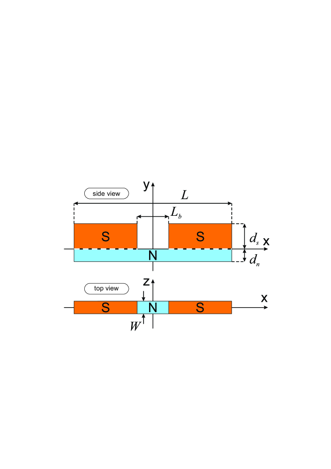
This problem is inherent for commonly used sandwich-type Josephson junctions. However, it can be circumvented by modification of the weak link region geometry with corresponding redistribution of current flowing therein [57, 58, 59, 60, 61]. An example of such solution is the SN-N-NS junction in the form of variable thickness bridge [62, 63, 64, 65, 66, 67, 68] presented in Fig. 1. Here a high current density in the bridge is lowered due to the current spread all over the area under the electrodes. The latter is owing to the finite transparency of SN interfaces [66, 69, 70, 71].
Metals with relatively large decay length are preferred to obtain high critical current value of SN-N-NS junction. Unfortunately, such metals generally possess relatively small resistivity, since while . However, if the thickness of N layer is smaller than the decay length, , then the suppression parameter is decreased [72] proportionally to their ratio,
| (3) |
corresponding to the decreased number of normal electrons diffusing from N to S. Thus, the SN-N-NS structure size ratio, , seems to be optimal choice to provide both: high critical current and normal state resistance of the junction.
Below we consider SN-N-NS junction with specified ratio of geometrical parameters as the promising candidate for scaling, since the decay length, , of the broadly utilized metals, like Al or Cu, lies in the range of a few tens of nanometers.
III Calculation of SN-N-NS junction supercurrent
Our model of SN-N-NS junction contains a normal metal film connecting two massive superconducting electrodes of the length, each, located at the distance from the center of this film, see Fig. 1. The total length of the junction is . In the calculation of the critical current, we suppose that condition of dirty limit is fulfilled for all metals, the critical temperature of N material is equal to zero and its width, , and thickness, , are much smaller than Josephson penetration depth, , and decay length, , respectively.
The proximity effect in this system can be considered in the frame of Usadel equations [73], which in the N film have the form,
| (4) |
Here are modified Usadel Green’s functions, and are Matsubara frequencies, is integer. are normalized on .
We apply standard boundary conditions at the edges of the structure [74] and Kupriyanov-Lukichev boundary condition [20] at SN interfaces. The conditions, , [72], permit us to neglect the suppression of superconductivity in the S film due to proximity effect even in the case of fully transparent SN interfaces, and also allows considering functions independent on the coordinate , in the first approximation on the parameter .
By integration of equations (4) over the coordinate , we obtain the equations,
| (5) |
for the region of electrodes, , where , is suppression parameter, is specific resistance of SN interface, are modified Usadel Green’s functions normalized on , . In the area of the bridge we have the following equations,
| (6) |
The solution of the problem is simplified in the limit of a small gap between superconducting electrodes, . We also suppose that in the practically interesting case, the length of superconducting electrodes is much larger than the characteristic scale, , which arise in the frame of analytical solution of the problem [74]. This characteristic scale is in the limit of small for arbitrary normalized temperature, . In the opposite limit of large , it is at small temperatures and at .
Under these assumptions, we obtain [74] the following expression for the product of superconducting current, , across the junction and its normal state resistance, ,
| (7) |
where , C are the constants determined by matching solutions in the ranges of electrodes and the bridge [74], and is the real part of the functions , while
| (8) |
is the sum [75] of the resistance of the bridge, , and the resistances of two SN interfaces, ,
In the limit of small suppression parameter,
(rigid boundary conditions), the expression (7) for supercurrent takes the following form,
| (9) |
where , is the magnitude of superconducting order parameter normalized on , is superconducting phase difference across the junction, and
For a vanishingly small suppression, , the expression (9) transforms into the formula obtained by Kulik and Omelyanchuk (KO-1) [76].
In the opposite limit of large ,
expression (7) transforms into
| (10) |
where is mainly determined by the resistance of SN interfaces.
IV product of SN-N-NS junction
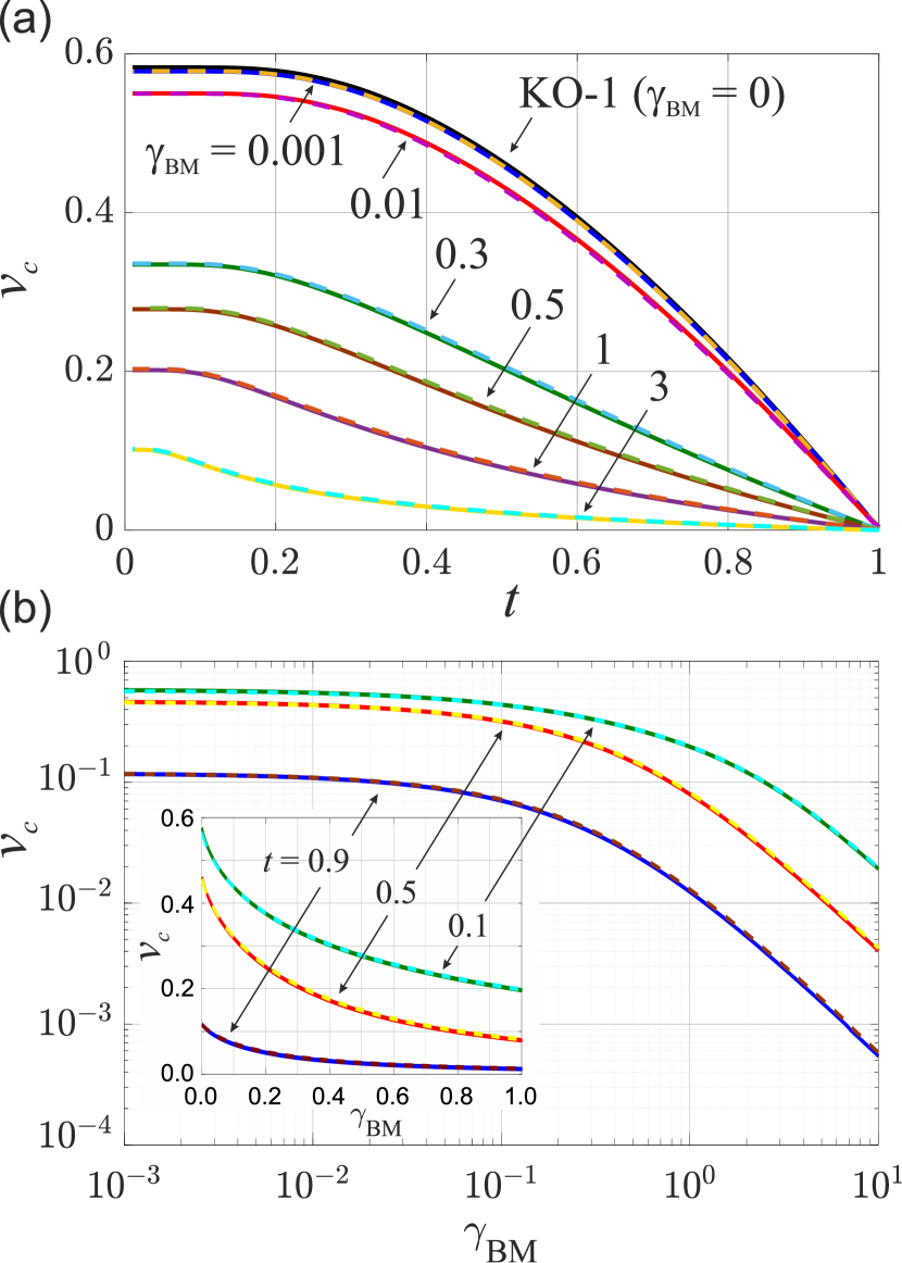
Characteristic voltage of SN-N-NS junction can be obtained directly from expression (7) and its limiting cases (9), (10). Fig. 2(a) shows normalized product, (where ), as a function of normalized temperature, . The normalizing coefficient value is mV for niobium critical temperature, K. The bridge length is . The curves obtained in both limits are well consistent. The presented dependencies are limited from above by the curve obtained using KO-1 expression [76] for as expected. The temperature corresponding to characteristic voltage drop by 20% from its maximum value decreases from at small suppression, , to at .
Fig. 2(b) presents dependence for different temperatures in double logarithmic scale. Inset shows these dependencies for . The characteristic voltage increases with the temperature decrease, in accordance with Fig. 2(a). For the commonly used temperature, , the characteristic voltage drops from its maximum value, , by 20% at , and becomes halved at . Starting from , the characteristic voltage falls as with . The decrease of the characteristic voltage with the suppression parameter increase is slower with the temperature decrease.
In the considered approximation, the characteristic voltage is nearly independent on the length of the bridge up to for arbitrary . The critical current, , is the larger the smaller are and . The current flowing through the junction () must not destroy the superconductivity in its electrodes. Below, we formulate the restriction on geometrical parameters of SN-N-NS structure coming from this requirement.
V Limitation on the current in superconducting electrodes
In accordance with experimental data obtained in MIT LL [12], a Nb strip with thickness, nm, and width, nm, possesses the critical current density, A/cm2 so that the critical current is mA at K. With an increase of the width, the critical current grows proportional to while with decrease below 250 nm, falls linearly with ,
| (11) |
where nm is a doubled thickness of the contaminated surface layer.
The linear dependence of the critical current on the width means that in the interesting for us range of the thickness, nm, the supercurrent is distributed uniformly over the film width. This fact allows us to seek the solution of the Usadel equations in the depth of the electrodes in the form independent on coordinate (see Fig. 1). Here is an independent on and constant, which is proportional to superfluid velocity. By assuming further that the supercurrent flowing through the SN electrodes is significantly less than the depairing current, we find functions from the solution of the proximity effect problem between superconducting and thin normal films,
For supercurrent densities, and , in the S and N films we get
| (12) |
| (13) |
where parameter in (12), (13),
| (14) |
is determined by the magnitude of the full current, , flowing through the SN electrodes, while in (14) is the ratio of the currents flowing through the N and S films,
| (15) |
so that .
At , the Matsubara frequencies are larger than We can neglect in comparison with when estimating the magnitudes of sums in (15) and get,
The current flowing through the S film must be small in comparison with S-film critical current,
| (16) |
where is the desired smallness coefficient. The magnitude of in (16) can be obtained from the data presented in Fig. 2, . Since and , the restriction (16) transforms into
| (17) |
where the coefficient for niobium is
| (18) |
We should note that for the ratio of the currents flowing through the N and S films is small, , and so .
VI Heat balance

An important requirement to the design of circuits based on the SN-N-NS junction is that the normal component, , of the total current must not lead to overheating of the SN-N-NS structure. Here we calculate the power dissipated in the junction during a clock period of a digital circuit and the power that can be absorbed by the junction environment. Then we evaluate the heating of niobium-copper SN-N-NS structure.
VI.1 Dissipated and absorbed power
The heating effect arises due to Joule dissipation. The energy dissipated during the junction switching, , can be estimated as
| (19) |
where is a voltage drop across the junction and . By assuming that the phase increase rate is and that the junction is switching once in a clock period, , we obtain the dissipated energy and average dissipated power,
| (20) |
The energy is transferred to normal electrons located in the region of concentration of the electric field which includes the bridge between SN electrodes. The hot electrons may diffuse from the heated region on the characteristic time scale For a typical value of Fermi velocity, m/s, electronic mean free path, nm, and the bridge length, nm, a rough estimation of gives the value s. This is an order larger than the scattering time, s.
Such a short value of means that for a time equal to a clock period lying in picosecond time scale, hot electrons diffuse along the N film into the SN electrodes over a distance of the order of the current leakage length, . This process is shown schematically by the red arrows in Fig. 3.
Within the standard model of electron energy relaxation, the electron-electron collision rate is assumed to be large so that the electrons maintain an equilibrium distribution characterized by the temperature, , which is different from the lattice temperature . The hot electrons may relax the excess energy making use of the two channels schematically shown in Fig. 3 by yellow and blue arrows.
The first channel for relaxation is the diffusion of hot electrons into superconducting electrodes. The heat conductance of the SN interface with small specific boundary resistance, , is given by the expression [77]
| (21) |
where is the effective area through which the heat flow takes place. For a finite transparency of SN interface , the area
The second channel is the transfer of excess energy to phonons. In dirty metals, the rate of this process , is given by [78]
| (22) |
| (23) |
where is the density of states at Fermy level, are longitudinal and transverse speeds of sound, is the mass density, is Fermi momentum, is electron mass, is the Riemann zeta function. Expression (22) can be rewritten via the thermal conductance per unit volume
| (24) |
where , is the local temperature of phonon subsystem in the heated segment.
The process of energy transformation from hot electrons to phonons occurs approximately in a volume marked by a violet arrow in Fig. 3.
Further phonon heat propagation along the N film can be described similar to the heat spread in an infinite rod from the inner heated segment, , which has a temperature exceeding the temperature of its ends in the initial moment,
| (25) |
where is the error function, and are thermal conductivity and thermal capacity of the N metal.
During a clock period, decreases from its initial value down to
| (26) |
The product determines the characteristic scale of the heat propagation.
The excess phonon temperature may further relax to the substrate (see green arrows in Fig. 3). The power transfer from the phonons in the normal metal to the substrate is given by the Kapitza coupling [79]
| (27) |
where depends on the materials, and is the effective interface area of the heat transfer marked by brown arrow in Fig. 3.
VI.2 Heating of SN-N-NS structures based on Nb/Cu material combination
The SN-N-NS variable thickness bridge proposed in this work can be fabricated using commonly used materials like Nb, MoRe, V as a superconductor and Cu, Au, Al as a normal metal. Below, we estimate the parameters of NbCu-Cu-CuNb structure in accordance with the restriction (17) and then calculate its heating assuming the clock period, ps (clock frequency, GHz).
Substitution of the typical values [80] of normal resistivity cm, decay length nm for Cu and cm for Nb into the obtained restriction on the critical current (17) shows that the inequality can be fulfilled already for at with if , nm, and nm. Here is naturally implemented at the interface of the considered materials.
For we obtain (see Fig. 2) so that mV, mA and . The dissipated energy during a clock period is aJ and therefore the dissipated power is
| (28) |
The specific boundary resistance is m2. By putting further K and in (21), we get the power flowing to the S films across SN interfaces,
| (29) |
where W/K.
By substituting the typical Cu parameters, m/s, kg/m km/s, km/s, K, nm, kg, J into (24) and taking into account that the energy exchange between hot electrons and phonons occurs inside the volume of the order of , we get the power transfer to phonons,
| (30) |
where W/K.
Further power transfer between the normal metal and the substrate phonons is given by the Kapitza coupling (27). The coefficient at Cu/Si interface approximately equals [81, 82, 83] to W m-2K-4. By taking [84, 85, 86] the thermal conductivity, W/m K, and thermal capacity, J/kg, for Cu, we get nm and (27) reads
| (31) |
where W/K.
In accordance with the heat balance described in the previous section, the power dissipated in the junction can be absorbed by the S-electrodes and the phonons of the N-film with subsequent partial power transfer into the substrate. Since , one can estimate the heating of the structure as follows,
| (32) |
Such temperature increase can lead to a slight decrease in the value of the critical current by the amount
| (33) |
see Fig. 2(a). The obtained deviation of the critical current seems acceptable in the view of standard optimization of the critical currents of Josephson junctions in digital circuits within the margins and standard technological critical current spread, .
The estimations (32), (33) show that in the temperature range of interest, , hot electrons effectively diffuse from the weak-link region into massive superconducting films, thereby eliminating the effect of the nonequilibrium state of the electronic subsystem on the mode of operation of SN-N-NS junction. It is necessary to mention that the lowering of the operation temperature leads to exponential suppression of the heat transfer channel from hot electrons to S electrodes. This can lead to the noticeable difference between electron and phonon temperatures, especially in mK temperature range.
VII Discussion
In summary, we argue that SN-N-NS junctions with variable thickness bridge geometry are promising for miniaturization. The presented theoretical analysis shows that the junction value reaches sub-millivolt level even when the rigid boundary conditions are not fulfilled at the SN interfaces. According to the obtained analytical expressions, the junction current-phase relation is close to a sinusoidal one at the operation temperature, . This allows the use of standard computer-aided design tools for superconducting digital circuit simulations.
The suppression parameter value, , can be taken as the upper threshold for the fabrication of Josephson junctions intended for operation at liquid helium temperature, K. The corresponding normalized characteristic voltage, , turns into mV and characteristic frequency, GHz. Since the clock frequency of complex circuits is usually a fraction of the characteristic one, the chosen value of provides the possibility of operation with frequencies up to several tens of GHz.
Based on available experimental data [12] we argue that the optimal width of SN-N-NS structure lays nearby nm. For a pair of materials like Nb and Cu, for nm, nm and nm, the characteristic voltage, mV, is achieved for mA and .
An increase of leads to undesirable inhomogeneity of the supercurrent distribution in the S electrodes. Its decrease results in the fast suppression of the S-film critical current. The use of additional technological steps aimed at the decrease of SN interface transparency may be required to decrease the junction critical current density in this case.
One of possible ways of controllable reduction of the SN interface transparency is the technique that has proved itself in the fabrication of Nb/Al-AlOx/Nb tunnel junctions [3, 15, 16, 13]. Here a Nb/Al sandwich can be used as a normal metal. A thin nonsuperconducting Nb film plays the role of a buffer layer. The subsequent growth of Al on such a buffer can contribute to the formation of an atomically smooth free surface of Al which provides predominantly mirror reflection of conducting electrons. The required Nb/Al boundary transparency, , can be achieved either naturally [69, 87] or by using the aluminum oxidation regime previously used in the fabrication of high- tunnel junctions [24]. Contrary to double barrier devices, in SN-N-NS junctions the two SN interfaces are oxidised under the same conditions thus keeping the symmetry of the structure.
The decrease of the transparency of the SN interfaces corresponds to a decrease in the characteristic voltage in proportion to and in the critical current in proportion to . Ultimately, the width limitations is determined by the quality of the edges of the superconducting electrodes. In the presence of “dead” edges nm wide, the width can hardly be less than nm.
An effective area of SN-N-NS junction, , can be determined according to the length within which the dominating heat transfer from hot electrons to superconducting films takes place, . Thus for so that with nm we obtain nm2. This is close to the area of semiconductor transistor, , fabricated in the frame of a 40 nm technological process, under the assumption that , where is the minimum feature size [88].
Acknowledgements.
The authors are grateful to D.V. Averin for fruitful discussions. Theoretical analysis of the considered SN-N-NS junction (Sections I - V) was supported by grant No. 20-12-00130 of the Russian Science Foundation. The study of the heat balance (Section VI) was performed according to the Development program of the Interdisciplinary Scientific and Educational School of Lomonosov Moscow State University ”Photonic and Quantum technologies. Digital medicine”, and the plan of scientific research of the SINP MSU .References
- Moore [2003] G. E. Moore, No exponential is forever: but ”Forever” can be delayed!, in IEEE International Solid-State Circuits Conference, 2003. Digest of Technical Papers. ISSCC (2003).
- Holmes et al. [2013] D. S. Holmes, A. L. Ripple, and M. A. Manheimer, Energy-efficient superconducting computing-power budgets and requirements, IEEE Trans. Appl. Supercond. 23, 1701610 (2013).
- Tolpygo [2016] S. K. Tolpygo, Superconductor digital electronics: Scalability and energy efficiency issues, Low Temp. Phys. 42, 361 (2016).
- Soloviev et al. [2017] I. I. Soloviev, N. V. Klenov, S. V. Bakurskiy, M. Y. Kupriyanov, A. L. Gudkov, and A. S. Sidorenko, Beyond Moore’s technologies: operation principles of a superconductor alternative, Beilstein J. Nanotechnol 8, 2689 (2017).
- Bhushan et al. [2020] M. Bhushan, P. Bunyk, M. Cuthbert, E. DeBenedictis, R. L. Fagaly, P. Febvre, C. Fourie, M. Frank, D. Gupta, A. Herr, D. S. Holmes, T. Humble, A. L. de Escobar, C. McGeoch, N. Missert, P. Mueller, O. Mukhanov, K. Nemoto, S. P. Rao, B. Patra, B. Plourde, N. Pugach, B. Tyrrell, T. Vogelsang, F. Wilhelm-Mauch, and N. Yoshikawa, IRDS 2020: Cryogenic Electronics and Quantum Information Processing, https://irds.ieee.org/editions/2020 (2020), part of IEEE International Roadmap for Devices and Systems.
- [6] E. P. DeBenedictis, New design principles for cold, scalable electronics, available at http://www.debenedictis.org/erik/Cryo_FPGA_2LAL/DPfC_51.pdf.
- Mukhanov [2011] O. A. Mukhanov, 100 years of superconductivity (Taylor & Francis: London, United Kingdom, 2011) Chap. History of Superconductor Analog-to-Digital Converters, pp. 440–458.
- Mukhanov [2015] O. A. Mukhanov, Applied superconductivity: Handbook on devices and applications (Wiley-VCH Verlag GmbH & Co. KGaA: Weinheim, Germany, 2015) Chap. Superconductor Digital Electronics, pp. 1–28.
- Mukhanov et al. [2004] O. A. Mukhanov, D. Gupta, A. M. Kadin, and V. K. Semenov, Superconductor analog-to-digital converters, Proc. IEEE 92, 1564 (2004).
- Nagasawa et al. [1999] S. Nagasawa, H. Numata, Y. Hashimoto, and S. Tahara, High-frequency clock operation of Josephson 256-word/spl times/16-bit RAMs, IEEE Trans. Appl. Supercond. 9, 3708–3713 (1999).
- [11] Cryogenic Computing Complexity (C3), available at https://www.iarpa.gov/index.php/research-programs/c3.
- Tolpygo et al. [2021] S. K. Tolpygo, V. Bolkhovsky, R. Rastogi, S. Zarr, E. Golden, T. J. Weir, L. M. Johnson, V. K. Semenov, and M. A. Gouker, A 150-nm process node of an eight-Nb-layer fully planarized process for superconductor electronics, in Applied Superconductivity Conference, ASC 2020 Virtual Conference, 49, Vol. 14 (Superconductivity News Forum (SNF), 2021) pp. STP669 Wk1EOr3B–01, available: https://snf.ieeecsc.org/issues/snfissue-no-49-march-2021.
- Tolpygo et al. [2019] S. K. Tolpygo, V. Bolkhovsky, R. Rastogi, S. Zarr, A. L. Day, E. Golden, T. J. Weir, A. Wynn, and L. M. Johnson, Advanced fabrication processes for superconductor electronics: Current status and new developments, IEEE Trans. Appl. Supercond. 29, 1102513 (2019).
- Tolpygo et al. [2016] S. K. Tolpygo, V. Bolkhovsky, T. J. Weir, A. Wynn, D. E. Oates, L. M. Johnson, and M. A. Gouker, Advanced fabrication processes for superconducting very large scale integrated circuits, IEEE Trans. Appl. Supercond. 26, 1 (2016).
- Tolpygo et al. [2017] S. K. Tolpygo, V. Bolkhovsky, S. Zarr, T. J. Weir, A. Wynn, A. L. Day, L. M. Johnson, and M. A. Gouker, Properties of unshunted and resistively shunted Nb/AlOx-Al/Nb Josephson junctions with critical current densities from 0.1 to 1 mA/m2, IEEE Trans. Appl. Supercond. 27, 1100815 (2017).
- Tolpygo et al. [2018] S. K. Tolpygo, V. Bolkhovsky, D. E. Oates, R. Rastogi, S. Zarr, A. L. Day, T. J. Weir, A. Wynn, and L. M. Johnson, Superconductor electronics fabrication process with MoNx kinetic inductors and self-shunted Josephson junctions, IEEE Trans. Appl. Supercond. 28, 1100212 (2018).
- Semenov et al. [2019] V. K. Semenov, Y. A. Polyakov, and S. K. Tolpygo, Very large scale integration of Josephson-junction-based superconductor random access memories, IEEE Trans. Appl. Supercond. 29, 1302809 (2019).
- Kupriyanov et al. [1999] M. Y. Kupriyanov, A. Brinkman, A. A. Golubov, M. Siegel, and H. Rogalla, Double-barrier Josephson structures as the novel elements for superconducting large-scale integrated circuits, Phys. C 326 – 327, 16 (1999).
- Brinkman et al. [2001] A. Brinkman, D. Cassel, A. A. Golubov, M. Y. Kupriyanov, M. Siegel, and H. Rogalla, Double-barrier Josephson junctions: Theory and experiment, IEEE Trans. Appl. Supercond. 11, 1146 (2001).
- Kuprianov and Lukichev [1988] M. Y. Kuprianov and V. F. Lukichev, Effect of boundary transparency on critical current in dirty SS’S structures, Sov. Phys. JETP 67, 1163 (1988).
- Galaktionov and Zaikin [2002] A. Galaktionov and A. Zaikin, Quantum interference and supercurrent in multiple-barrier proximity structures, Phys. Rev. B 65, 184507 (2002).
- [22] In the first RSFQ integrated circuits [89] made on the basis of double-barrier SINIS structures, the critical current density was set to a nominal value of A/m2, with values of the characteristic voltage equal to or larger than V. Such high values of the were due to the fact that, when evaluated, the normal resistance was determined in the region of low voltages in the initial quasilinear part of the I-V characteristic and was a dynamic resistance which magnitude exceeded at least by order of magnitude the true normal resistance of the structure [90].
- Born et al. [2003] F. Born, D. Cassel, K. Ilin, A. Klushin, M. Siegel, A. Brinkman, A. Golubov, M. Kupriyanov, and H. Rogalla, Transport properties of SINIS junctions with high-current density, IEEE Trans. Appl. Supercond. 13, 1079 (2003).
- Tolpygo et al. [2003] S. Tolpygo, A. Brinkman, A. Golubov, and M. Kupriyanov, Transport properties of SINIS junctions with high-current density, IEEE Trans. Appl. Supercond. 13, 138 (2003).
- Kieler et al. [2002] O. Kieler, R. Behr, F. Muller, H. Schulze, J. Kohlmann, and J. Niemeyer, Improved 1 V programmable Josephson voltage standard using SINIS junctions, Physica C: Superconductivity 372–376, Part 1, 309 (2002).
- Behr et al. [2005] R. Behr, J. M. Williams, P. Patel, T. J. B. M. Janssen, T. Funck, and M. Klonz, Synthesis of precision waveforms using a SINIS Josephson junction array, IEEE Trans. Appl. Supercond. 54, 612 (2005).
- Mueller et al. [2007] F. Mueller, R. Behr, L. Palafox, J. Kohlmann, R. Wendisch, and I. Krasnopolin, Improved 10 V SINIS series arrays for applications in AC voltage metrology, IEEE Trans. Appl. Supercond. 17, 649 (2007).
- Gudkov et al. [2012] A. L. Gudkov, M. Y. Kupriyanov, and A. N. Samus, Properties of planar Nb/-Si/Nb Josephson junctions with various degrees of doping of the -Si layer, JETP 114, 818–829 (2012).
- Gudkov et al. [1988] A. L. Gudkov, M. Y. Kupriyanov, and K. K. Likharev, Properties of Josephson junctions with amorphous-silicon interlayers, Sov. Phys. JETP 67, 1478 (1988).
- Kulikov et al. [1991] V. A. Kulikov, L. V. Matveets, A. L. Gudkov, V. N. Laptev, and V. I. Makhov, A mm-wave radiometer with planar Nb/-Si/Nb Josephson junction, IEEE Trans. Magn. MAG-27, 2468 (1991).
- Baek et al. [2006a] B. Baek, P. D. Dresselhaus, and S. P. Benz, Co-sputtered amorphous NbxSi(1-x) barriers for Josephson-junction circuits, IEEE Trans. Appl. Supercond. 16, 1966 (2006a).
- Baek et al. [2006b] B. Baek, P. D. Dresselhaus, and S. P. Benz, Thermal stability of Nb/-NbxSi1-x/Nb Josephson junctions, Phys. Rev. B 75, 054514 (2006b).
- Olaya et al. [2008] D. Olaya, B. Baek, P. D. Dresselhaus, and S. P. Benz, High-speed Nb/Nb-Si/Nb Josephson junctions for superconductive digital electronics, IEEE Trans. Appl. Supercond. 18, 1797 (2008).
- Olaya et al. [2009] D. Olaya, P. D. Dresselhaus, S. P. Benz, J. Bjarnason, and E. N. Grossman, Amorphous Nb-Si barrier junctions for voltage standard and digital applications, IEEE Trans. Appl. Supercond. 19, 144 (2009).
- Chong et al. [2009] Y. Chong, S. I. Park, and K. Kim, Sputter deposition of MoSi2 film as a barrier for Nb-based Josephson junction, IEEE Trans. Appl. Supercond. 19, 238 (2009).
- Muller et al. [2013] F. Muller, T. Scheller, R. Wendisch, R. Behr, O. Kieler, L. Palafox, and J. K. and, NbSi barrier junctions tuned for metrological applications up to 70 GHz: 20 V arrays for programmable Josephson voltage standards, IEEE Trans. Appl. Supercond. 23, 1101005 (2013).
- Olaya et al. [2014] D. Olaya, P. D. Dresselhaus, and S. P. Benz, 300-GHz operation of divider circuits using high-jc Nb/NbxSi1-x/Nb Josephson junctions, IEEE Trans. Appl. Supercond. 25, 1101005 (2014).
- Olaya et al. [2015] D. Olaya, P. D. Dresselhaus, and S. P. Benz, 300-GHz operation of divider circuits using high- Nb/NbxSi1-xNb Josephson junctions, IEEE Trans. Appl. Supercond. 25, 1101005 (2015).
- Cao et al. [2018] W. Cao, H. Chen, T. Liang, J. Li, X. Kong, T. Sun, Q. Zhong, X. Wang, L. Wang, and Y. Zhong, Fabrication and characterization of SQUIDs with Nb/NbxSi/Nb junctions, IEEE Trans. Appl. Supercond. 28, 1602204 (2018).
- Olaya et al. [2019a] D. Olaya, M. Castellanos-Beltran, J. Pulecio, J. Biesecker, S. Khadem, T. Lewitt, P. Hopkins, P. Dresselhaus, and S. Benz, Planarized process for single-flux-quantum circuits with self-shunted Nb/NbxSi1-x/Nb Josephson junctions, IEEE Trans. Appl. Supercond. 29, 1101708 (2019a).
- Haygood et al. [2019] I. W. Haygood, E. R. J. Edwards, A. E. Fox, M. R. Pufall, M. L. Schneider, W. H. Rippard, P. D. Dresselhaus, and S. P. Benz, Characterization of uniformity in Nb/NbxSi1-x/Nb Josephson junctions, IEEE Trans. Appl. Supercond. 29, 1103505 (2019).
- Olaya et al. [2019b] D. Olaya, M. Castellanos-Beltran, J. Pulecio, J. Biesecker, S. Khadem, T. Lewitt, P. Hopkins, P. Dresselhaus, and S. Benz, Planarized process for single-flux-quantum circuits with self-shunted Nb/NbxSi1-x/Nb Josephson junctions, IEEE Trans. Appl. Supercond. 29, 1101708 (2019b).
- Ivanov et al. [1981] Z. G. Ivanov, M. Y. Kupriyanov, K. K. Likharev, S. V. Meriakri, and O. V. Snigirev, Boundary-conditions for the Usadel and Eilenberger equations, and properties of dirty SNS sandwich-type junctions, Sov. J. Low. Temp. Phys. 7, 274 (1981).
- Kupriyanov and Lukichev [1982] M. Y. Kupriyanov and V. F. Lukichev, The influence of proximity effect in electrodes on the stationary properties of S-N-S Josephson structures, Sov. J. Low. Temp. Phys. 8, 526 (1982).
- Fritzsch et al. [1998] L. Fritzsch, M. Schubert, G. Wende, and H.-G. Meyer, Superconductor-normal metal-superconductor Josephson junctions with Ti interlayer, Appl. Phys. Lett. 73, 1583 (1998).
- Popel et al. [2000] R. Popel, D. Hagedorn, T. Weimann, F.-I. Buchholz, and J. Niemeyer, Superconductor-normal metal-superconductor process development for the fabrication of small Josephson junctions in ramp type configuration, Supercond. Sci. Technol. 13, 148 (2000).
- Hagedorn et al. [2001] D. Hagedorn, R. Dolata, R. Popel, F.-I. Buchholz, and J. Niemeyer, Development of sub-micron SNS ramp-type Josephson junctions, IEEE Trans. Appl. Supercond. 11, 1134 (2001).
- Schubert et al. [2001] M. Schubert, L. Fritzsch, G. Wende, and H.-G. Meyer, SNS junction on Nb-Ti base for microwave circuits, IEEE Trans. Appl. Supercond. 11, 1066 (2001).
- Hagedorn et al. [2002] D. Hagedorn, R. Dolata, F.-I. Buchholz, and J. Niemeyer, Properties of SNS Josephson junctions with HfTi interlayers, Physica C 372–376, Part 1, 7 (2002).
- Dresselhaus et al. [2003] P. D. Dresselhaus, Y. Chong, J. H. Plantenberg, and S. P. Benz, Stacked SNS Josephson junction arrays for quantum voltage standards, IEEE Trans. Appl. Supercond. 13, 930 (2003).
- Hagedorn et al. [2003] D. Hagedorn, M. Khabipov, R. Dolata, F. I. Buchholz, and J. Niemeyer, An SNS technology process for ramp junction based digital superconducting circuits, IEEE Trans. Appl. Supercond. 13, 1096 (2003).
- Schubert et al. [2005] M. Schubert, T. May, G. Wende, and H. G. Meyer, A cross-type SNS junction array for a quantum-based arbitrary waveform synthesizer, IEEE Trans. Appl. Supercond. 15, 829 (2005).
- Hagedorn et al. [2006] D. Hagedorn, O. Kieler, R. Dolata, R. Behr, F. Muller, J. Kohlmann, and J. Niemeyer, Modified fabrication of planar sub-m superconductor-normal metal-superconductor Josephson junctions for use in a Josephson arbitrary waveform synthesizer, IEEE Trans. Appl. Supercond. 19, 294 (2006).
- Nagel et al. [2011] J. Nagel, O. F. Kieler, T. Weimann, R. Woelbing, J. Kohlmann, A. B. Zorin, R. Kleiner, D. Koelle, and M. Kemmler, Superconducting quantum interference devices with submicron Nb/HfTi/Nb junctions for investigation of small magnetic particles, Appl. Phys. Lett. 99, 032506 (2011).
- Zubkov and Kupriyanov [1983] A. Zubkov and M. Kupriyanov, Effect of depairing in electrodes on the stationary properties of weak links, Sov. J. Low Temp. Phys. 5, 279 (1983).
- Kupriyanov [1992] M. Kupriyanov, Effect of a finite transmission of the insulating layer on the properties of SIS tunnel-junctions, JETP Letters 56, 399–405 (1992).
- Likharev [1971] K. K. Likharev, Vortex motion and the Josephson effect in superconducting thin bridges, Zh. Eksp. Teor. Fiz. 61, 1700 (1971), [Sov. Phys. JETP 34, 906 (1972)].
- Likharev and Yakobson [1975] K. K. Likharev and L. A. Yakobson, Dynamical properties of superconducting filaments of finite length, Zh. Eksp. Teor. Fiz. 68, 1150 (1975), [Sov. Phys. JETP 41, 570-575 (1976)].
- Likharev [1976] K. K. Likharev, The relation for SNS bridges of variable thickness, Pis’ma Zh. Tekh. Fiz. 2, 29 (1976), [Sov. Tech. Phys. Lett. 2, 12 (1976)].
- Dubos et al. [2001] P. Dubos, H. Courtois, B. Pannetier, F. K. Wilhelm, A. D. Zaikin, and G. Schön, Josephson critical current in a long mesoscopic S-N-S junction, Phys. Rev. B 63, 064502 (2001).
- Marychev and Vodolazov [2020] P. M. Marychev and D. Y. Vodolazov, A Josephson junction based on a highly disordered superconductor/low-resistivity normal metal bilayer, Beilstein J. Nanotechnol. 11, 858–865 (2020).
- Warlaumont et al. [1979] J. M. Warlaumont, J. C. Brown, T. Foxe, and R. A. Buhrman, Microwave-enhanced proximity effect in superconductor-normal-metal-superconductor microjunctions, Phys. Rev. Lett. 43, 169 (1979).
- van Dover et al. [1981] R. B. van Dover, A. de Lozanne, and M. R. Beasley, Superconductor‐normal‐superconductor microbridges: Fabrication, electrical behavior, and modeling, J. Appl. Phys. 52, 7327 (1981).
- Liengme et al. [1983] O. Liengme, P. Lerch, W. Liu, and P. Martinoli, Fabrication and electromagnetic properties of planar variable-thickness S-N-S microbridges, IEEE Tran. Magn. 19, 995 (1983).
- Nakano and Aomine [1983] H. Nakano and T. Aomine, Magnetic field dependence of critical currents in SNS bridges fabricated by direction of sputtering deposition and anodie oxidization, Jap. J. Appl. Phys. 26, 304 (1983).
- Sauvageau et al. [1985] J. Sauvageau, R. Ono, A. Jain, K. Li, and J. Lukens, Length dependent properties of SNS microbridges, IEEE Tran. Magn. 21, 854 (1985).
- Baryshev et al. [1989a] Y. Baryshev, A. Dmitriev, A. Krivospitsky, V. Lukichev, A. Orlikovsky, and K. Valiev, Josephson SNS microbridges fabricated by double electron beam lithography, Microelectronic Engineering 9, 385 (1989a).
- Baryshev et al. [1989b] Y. P. Baryshev, A. G. Vasil’ev, A. A. Dmitriyev, M. Y. Kupriyanov, V. F. Lukichev, I. Y. Luk’yanova, and I. S. Sokolova, Theoretical and experimental study of the Josephson effect in submicron SN-N-NS structures, Lithography in microelectronics 8, 187 (1989b).
- Zehnder et al. [1999] A. Zehnder, P. Lerch, S. P. Zhao, T. Nussbaumer, E. C. Kirk, and H. R. Ott, Proximity effects in Nb/Al-AlOx-Al/Nb superconducting tunneling junctions, Phys. Rev. B 59, 8875 (1999).
- Baxter et al. [1999] D. V. Baxter, S. D. Steenwyk, J. Bass, and W. P. Pratt, Resistance and spin-direction memory loss at Nb/Cu interfaces, J. Appl. Phys. 85, 4545 (1999).
- Park et al. [2000] W. Park, D. V. Baxter, S. Steenwyk, I. Moraru, W. P. Pratt, and J. Bass, Measurement of resistance and spin-memory loss (spin relaxation) at interfaces using sputtered current perpendicular-to-plane exchange-biased spin valves, Phys. Rev. B 62, 1178 (2000).
- Golubov et al. [1983] A. A. Golubov, M. Y. Kupriyanov, and V. F. Lukichev, Influence of the proximity effect in the electrodes on the stationary properties of SN-N-NS variable-thickness bridges, Soviet Microelectronics 12, 180 (1983).
- Usadel [1970] K. D. Usadel, Generalized diffusion equation for superconducting alloys, Phys. Rev. Lett. 25, 507 (1970).
- [74] See supplementary material for details of the SN-N-NS junction supercurrent calculation.
- Karminskaya et al. [2010] T. Y. Karminskaya, A. A. Golubov, M. Y. Kupriyanov, and A. S. Sidorenko, Josephson effect in superconductor/ferromagnet structures with a complex weak-link region, Phys. Rev. B 81, 214518 (2010).
- Kulik and Omelyanchuk [1970] I. O. Kulik and A. N. Omelyanchuk, Contribution to the microscopic theory of the Josephson effect in superconducting bridges, JETP. Lett. 21, 96 (1970).
- Leivo et al. [1996] M. M. Leivo, J. P. Pekola, and D. V. Averin, Efficient peltier refrigeration by a pair of normal metal/insulator/superconductor junctions, Appl. Phys. Lett. 68, 1996 (1996).
- Nikolic et al. [2020] D. Nikolic, D. M. Basko, and W. Belzig, Electron cooling by phonons in superconducting proximity structures, Phys. Rev. B 102, 214514 (2020).
- Swartz and Pohl [1989] E. T. Swartz and R. O. Pohl, Thermal boundary resistance, Rev. Mod. Phys. 61, 605 (1989).
- Stolyarov et al. [2018] V. S. Stolyarov, T. Cren, C. Brun, I. A. Golovchanskiy, O. V. Skryabina, D. I. Kasatonov, M. M. Khapaev, M. Y. Kupriyanov, A. A. Golubov, and D. Roditchev, Expansion of a superconducting vortex core into a diffusive metal, Nat. Commun. 9, 2217 (2018).
- Roukes et al. [1985] M. L. Roukes, M. R. Freeman, R. S. Germain, R. C. Richardson, and M. B. Ketchen, Hot electrons and energy transport in metals at millikelvin temperatures, Phys. Rev. Lett. 55, 422 (1985).
- Wellstood et al. [1989] F. C. Wellstood, C. Urbina, and J. Clarke, Hot‐electron limitation to the sensitivity of the dc superconducting quantum interference device, Appl. Phys. Lett. 54, 2599 (1989).
- Kautz et al. [1993] R. L. Kautz, G. Zimmerli, and J. M. Martinis, Self‐heating in the coulomb‐blockade electrometer, J. Appl. Phys. 73, 2386 (1993).
- L.A.Novitskiy and Kogevnikov [1975] L.A.Novitskiy and I. Kogevnikov, Thermophysical properties of materials at low temperatures. Handbook (Moscow, publishing house ”Mechanical engineering”, 1975).
- Phillips [1971] N. E. Phillips, Low-temperature heat capacity of metals, Critical Reviews in Solid State and Material Sciences 2, 467 (1971).
- Pobell [2007] F. Pobell, Matter and Methods at Low Temperatures (Springer Berlin Heidelberg New York, 2007) p. 77.
- Brammertz et al. [2001] G. Brammertz, A. Poelaert, A. A. Golubov, P. Verhoeve, A. Peacock, and H. Rogalla, Generalized proximity effect model in superconducting bi- and trilayer films, J. Appl. Phys. 90, 355 (2001).
- Ansari et al. [2015] M. Ansari, H. Afzali-Kusha, B. Ebrahimi, Z. Navabi, A. Afzali-Kusha, and M. Pedram, A near-threshold 7T SRAM cell with high write and read margins and low write time for sub-20nm FinFET technologies, Integr. VLSI J. 50, 91 (2015).
- Balashov et al. [1998] D. Balashov, F.-I. Buchholz, H. Schulze, M. I. Khabipov, W. Kessel, and J. Niemeyer, Superconductor-insulator-normal- conductor-insulator-superconductor process development for integrated circuit applications, Supercond. Sci. Technol. 11, 1401 (1998).
- Brinkman et al. [2003] A. Brinkman, A. Golubov, H. Rogalla, F. Wilhelm, and M. Kupriyanov, Microscopic nonequilibrium theory of double-barrier Josephson junctions, Phys. Rev. B 68, 224513 (2003).