A growth diagram for chemical beam epitaxy of GaP1-xNx alloys on nominally -oriented GaP-on-Si substrates
Abstract
The compound GaP1-xNx is highly attractive to pseudomorphically integrate red light-emitting devices and photovoltaic cells with the standard Si technology because it is lattice matched to Si with a direct band gap of eV for . Here, we report on the chemical beam epitaxy of GaP1-xNx alloys on nominally -oriented GaP-on-Si substrates. The incorporation of N into GaP1-xNx was systematically investigated as a function of the growth temperature and the fluxes of the N and P precursors, 1,1-dimethylhydrazine (DMHy) and tertiarybutylphosphine (TBP), respectively. We found that the N mole fraction exhibits an Arrhenius behavior characterized by an activation energy of eV. With respect to the fluxes, we determined that the N mole fraction is linearly proportional to the flux of DMHy, and inversely proportional to the one of TBP. All results are summarized in a universal equation that describes the dependence of x on the growth temperature and the fluxes of the group-V precursors. The results are further illustrated in a growth diagram that visualizes the variation of x as the growth temperature and the flux of DMHy are varied. This diagram also shows how to obtain single-phase and flat GaP1-xNx layers, as certain growth conditions result in chemically phase-separated layers with rough surface morphologies. Last, our results demonstrate the feasibility of chemical beam epitaxy to obtain single-phase and flat GaP1-xNx layers with x up to about , a value well above the one required for the lattice-matched integration of GaP1-xNx-based devices on Si.
I Introduction
The incorporation of small amounts of N into GaP, besides decreasing the lattice parameter, induces an indirect-to-direct band gap transition well described by the band anticrossing model [1, 2]. Remarkably, for a N mole fraction , the ternary compound GaP1-xNx is lattice-matched to Si with a direct band gap of about eV at room temperature, making this material rather unique for the monolithic integration of pseudomorphic red-light emitters and III-V photovoltaic solar cells with the widespread, highly scalable and cost-effective Si technology [3, 4, 5, 6, 7, 8, 9, 10]. Nevertheless, despite of the great potential of this compound, commercial red-light emitting devices are still based on AlxInyGa1-x-yP alloys [11] and the efficiency of GaP1-xN on Si photovoltaic solar cells remains too low as to consider this material combination a competitive technology [8]. This situation arises from: (i) The challenging synthesis of GaP1-xN alloys with high structural perfection. Specifically, the material quality of dilute-nitride compounds is known to degrade as the N content and the layer thickness are increased, as reported for thin films and devices grown, for instance, by metal-organic vapor phase epitaxy (MOVPE) and plasma-assisted molecular beam epitaxy (PA-MBE) [3, 12, 13, 14, 15, 16]. (ii) The common use of highly misoriented ( ∘) instead of on-axis Si substrates to avoid the creation of anti-phase domains,[12, 17, 18] a solution that undermines the integration ofGaP1-xNx-based devices with the standards of Si technology.
Chemical beam epitaxy (CBE), an ultra-high-vacuum epitaxial growth technique characterized by the use of gaseous precursors in the form of molecular beams for both group-III and -V elements [19], offers important advantages over alternative methods for the synthesis of GaP1-xNx compounds. On the one hand, the ultra-high-vacuum environment enables the use of powerful techniques to optimize and monitor the growth, such as reflection high-energy electron diffraction (RHEED). On the other hand, as N is not produced by a radio-frequency N2 plasma source, there is no crystal-damage associated to the impingement of energetic ionized N species [20], a major issue in PA-MBE that enforces the realization of ex-situ rapid-thermal annealing treatments to improve the material quality [21, 20, 22, 16]. Furthermore, from technical and safety points of view, CBE is also advantageous as compared to PA-MBE because the residual gases can be easily extracted during and after the growth process. Therefore, it is possible to avoid the risks associated to the accumulation of hazardous P-containing materials inside the epitaxial reactor. So far, however, reports on the synthesis of GaP1-xNx compounds by CBE are scarce, limited to the analysis of individual growth parameters on the chemical composition, and restricted to the use of either bulk GaP or misoriented Si substrates [23, 24, 10]. There is thus the need of comprehensively exploring the chemical beam epitaxy of GaP1-xNx alloys on nominally -oriented Si substrates to elucidate the potential of CBE for monotonically integrating GaP1-xNx devices on Si.
In this work, we investigate the chemical beam epitaxy of GaP1-xNx alloys on CMOS-compatible GaP on Si substrates, as desired for the integration of III-V compounds on Si, with the aim of establishing how to control the chemical composition and properties of these compounds in CBE. Upon independently analyzing the influence of the growth temperature and the fluxes of the group-V precursors on the incorporation of N into GaP1-xNx, all results are summarized in a universal equation that we used to construct a growth diagram. This diagram, which illustrates the dependence of the chemical composition on the growth conditions as well as the impact of the growth parameters on both the chemical homogeneity and the surface morphology, can be used as a guide to control the properties of GaP1-xNx compounds grown by CBE. Finally, on the basis of the studies presented here, we conclude on the feasibility of CBE to produce chemically homogeneous and flat GaP1-xNx layers lattice matched to Si.
II Experimental
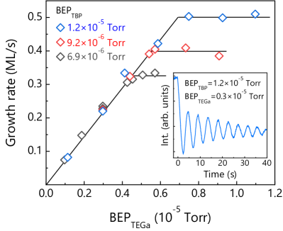
We prepared the samples in a Riber CBE32 system using triethylgallium (TEGa), tertiarybutylphosphine (TBP) and 1,1-dimethylhydrazine (DMHy) as gas sources for Ga, P and N, respectively. Low-temperature (120 ∘C) gas injectors were used for both TEGa and DMHy, while a high-temperature one (820 ∘C) was employed for TBP to increase its cracking efficiency, as attested by quadrupole mass spectrometry. The growth chamber is equipped with an infrared optical pyrometer for monitoring the substrate temperature, a 15 keV RHEED gun, and an ion gauge that can be placed at the position of the substrate holder during growth to assess the beam equivalent pressure (BEP) of each gas precursor, a magnitude directly proportional to its flux. In the cases of Ga and P, we previously correlated the BEP values of the gas precursors with their actual effective fluxes (i.e., the amount of material that is actually incorporated per time and area units) in equivalent growth rate units of monolayers per second (ML/s) by measuring the growth rate of GaP for different values of BEPTEGa and BEPTBP. We note that 1 ML corresponds to , where is the Si lattice constant, i. e., 1 ML atoms/cm2. The correlation between the BEP values and the fluxes is illustrated in Fig. 1, where the growth rate of GaP, extracted from the frequency analysis of RHEED intensity oscillations, is represented as a function of BEPTEGa for three different values of BEPTBP. As can be observed, the growth rate linearly increases with BEPTEGa (P-rich regime) until becoming limited by BEPTBP (Ga-rich regime). Further technical details about the CBE system can be found elsewhere [25].
All samples were grown on cm2 GaP-on-Si substrates diced from a 12" wafer purchased from. This wafer, despite its nominally exact orientation, exhibits a slight miscut of towards one of the four directions, as determined by high-resolution X-ray diffraction (HRXRD). The GaP layer, free of dislocations, stacking faults and twins, is 25 nm thick and possess a smooth surface (root mean square roughness of 0.3 nm) without anti-phase domains. The substrates were In-bonded onto Mo holders and outgassed under TBP supply inside the growth chamber at 610 ∘C until observing the appearance of a clear surface reconstruction. The latter reflects the complete thermal desorption of the native oxide layer formed on the purchased wafer due to air exposure. Upon desorbing the oxide, we prepared a 15 nm thick GaP buffer layer at 580 ∘C to planarize the surface and bury possible impurities. This layer was grown under P-rich growth conditions with BEP Torr and BEP Torr, values that correspond to fluxes of 0.5 and 0.22 ML/s, respectively (see Fig. 1). Under these conditions GaP grows layer-by-layer, as evidenced by the observation of strong RHEED intensity oscillations (see inset in Fig. 1). After the growth of the GaP buffer layer, GaP1-xNx was grown for min, which results in a thickness of about210 nm. As discussed below, different series of samples were prepared to independently investigate the impact of the growth temperature and the fluxes of DMHy and TBP on N incorporation taking as starting point the V/III ratio employed for the growth of the GaP buffer layer, i. e., .
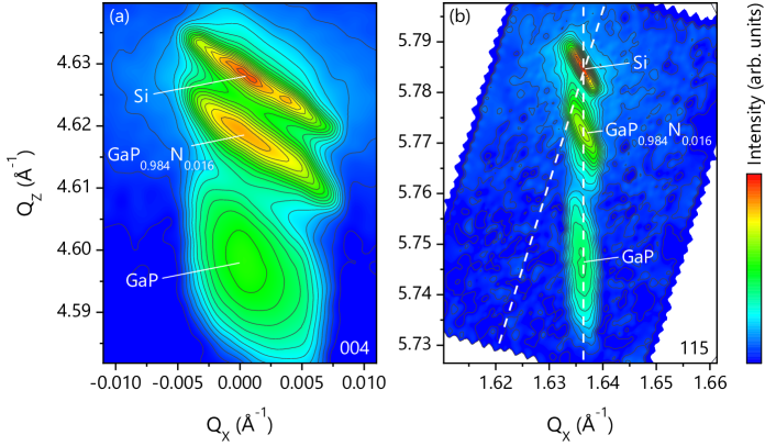
High-resolution X-ray diffraction measurements were performed with CuKα1 radiation (wavelength Å) using a BEDE D3 diffractometer equipped with a 4-bounce Si double-crystal monochromator and a Göbel mirror. Both reciprocal space maps (RSMs) and scans were acquired with a mm slit in front of the detector. All measurements were performed along the direction of the miscut. The chemical composition and the strain state of the layers were deduced from the peak locations in RSMs recorded along symmetrical and asymmetrical Bragg reflections. As can be observed in the exemplary RSMs shown in Fig. 2, we clearly resolve the GaP1-xNx, GaP and Si reflections. To calculate the chemical composition and the strain, we took into account the possible tilt of the epitaxial layers with respect to the normal of the Si substrate surface, , as described in Refs. 26, 27. The obtained values of are arcsec, i. e., one order of magnitude smaller than those reported for GaP layers grown on misoriented Si substrates [28]. The GaP1-xNx stiffness constants were estimated according to the Vegard’s law. The GaP and GaN stiffness constants and lattice parameters were taken from Ref. 29.
III Results and discussion
III.1 Effect of growth parameters on N incorporation
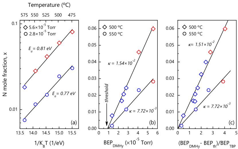
In this section, we systematically analyze the individual impact of the growth temperature and the fluxes of DMHy and TBP on the incorporation of N into GaP1-xNx. Figure 3(a) shows the N mole fraction x as a function of the growth temperature for BEP Torr and two different values of BEPDMHy, namely, and Torr. The N mole fractions shown in the figure are mean values, as some samples exhibit evidences of chemical phase separation (x values of phase-separated samples are shown using red color in Fig. 3). We will return to this point in section III.2. Regardless of the BEPDMHy value, we observe an exponential decrease of x with increasing growth temperature. Specifically, as the growth temperature is varied between 475 and 575 ∘C, x decreases from 0.03 to 0.008 for BEP Torr, and from 0.081 to 0.018 for BEP Torr. The maximum N mole fraction achieved here using DMHy as N source, 0.08, is significantly higher than the previous values reported for GaP1-xNx layers grown by CBE using either NH3[23] or monomethylhydrazine (MMHy)[24] ( for Ref.23 and 0.0189 for Ref.24). Returning to Fig. 3(a), the observed temperature dependencies of x are well described by Arrhenius laws. The fits to the experimental data included in the above figure yield activation energies of and eV for BEP and Torr, respectively. The activation energies are thus rather similar when taking into account the experimental uncertainties. Hence, the incorporation of N as a function of the growth temperature can be written as:
| (1) |
where is the Boltzmann’s constant, by using the mean activation energy value of E eV and a BEPDMHy dependent exponential prefactor A. In the present case, we found A for BEP Torr and A for BEP Torr. The decrease of x with the growth temperature is comparable to those reported for samples grown by plasma-assisted gas-source molecular beam epitaxy (GS-MBE) [30] and MOVPE using DMHy [31, 32]. In the case of MOVPE, the temperature dependence of x was also well described by Arrhenius laws, but with slightly higher activation energies, specifically, eV [31, 32]. In accordance to previous reports, we attribute the decreasing N content with increasing growth temperature to the desorption of N-related byproducts resulting from the dissociation of DMHy (NH2CH3, NH3 and NH2) and/or to the direct desorption of N atoms from the GaP1-xNx surface [33, 31, 32, 34].
Next, we investigate the influence of the impinging fluxes of DMHy and TBP on the incorporation of N. In principle, one would expect a dependence of x on the BEPs of DMHy and TBP given by:
| (2) |
where s1 and s2 are coefficients including both the sensitivity of BEP measurements to the particular precursor molecules (caused by their specific ionicity) and the incorporation efficiencies of N and P atoms with respect to the fluxes of DMHy and TBP, respectively [35]. Since dilute nitrides are characterized by small x values, , and Eq. (2) can thus be approximated by:
| (3) |
with representing the ratio between the N and P incorporation efficiencies with respect to the BEP values of DMHy and TBP. Notice that, according to Eq. (1), must depend on the growth temperature.
Let us see now whether the incorporation of N as a function of the impinging fluxes is actually well described by Eq. (3). Figure 3(b) presents the variation of the mean N mole fraction x with BEPDMHy at two different growth temperatures, 500 and 550 ∘C, using a constant flux of TBP given by BEP Torr. The experimental data show a nearly linear dependence with a temperature dependent slope. The values of derived from the fits are and for 500 and 550 ∘C, respectively. Consequently, within the investigated temperature range, N incorporation is about two orders of magnitude less efficient than P incorporation with respect to the BEP values of DMHy and TBP. Interestingly, the linear fits does not intercept the x-axis at zero, as predicted by Eq. (3). There is, however, a BEPDMHy threshold to overcome in order to incorporate a measurable amount of N. We attribute this threshold to the thermal desorption of N-reactive species and/or N atoms. On these basis, we rewrite the dependence of x on the impinging fluxes as:
| (4) |
where represents the above threshold. The values of extracted from the fits shown in Fig. 3(b) are and Torr for the series of samples prepared at 500 and 550 ∘C, respectively. In consequence, increases, as expected, with the growth temperature, but the variation is small when compared with the values ofBEPDMHy.
To further challenge Eq. (4), we plot in Fig. 3(c) x versus (BEPDMHy-BEPth)/BEPTBP for the samples shown in Fig. 3(b) as well as for three additional samples. These last three samples were grown at 500 ∘C with BEP Torr using different BEPTBP values than the one used to prepare the samples shown in Figs. 3(a) and 3(b), namely, , and Torr. The linear fits included in Fig. 3(c) demonstrate that Eq. (4) correctly describes all our growth data (the fit for the series prepared at 550 ∘C is analogous to the one presented in Fig. 3(b), but it is shown here again for the sake of completeness). The value derived for the samples grown at 500 ∘C, , is almost identical to one found before. Therefore, these results reinforce the validity of Eq. (4) to describe the dependence of x on the impinging fluxes for N mole fractions up to at least 0.06, i. e., the maximum x value shown in Fig. 3(c).
III.2 Phase separation
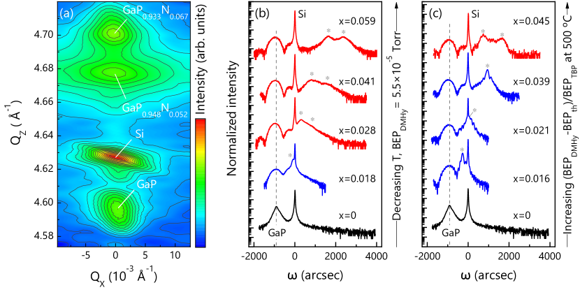
The N mole fractions shown in Fig. 3 are mean values because some GaP1-xNx layers are chemically phase separated, as discussed here. Blue and red data points in Fig. 3 correspond to single- and phase-separated samples, respectively. Single-phase samples are characterized by exhibiting a unique well-defined GaP1-xNx peak in RSMs, as exemplary illustrated in Fig. 2. In contrast, phase-separated samples exhibit two GaP1-xNx peaks as shown in Fig. 4(a) for a sample with a mean N mole fraction of grown at 500 ∘C with BEP Torr and BEP Torr. For this sample, the GaP1-xNx peaks detected in the RSM seem to be originated from regions with N mole fractions of and . In general, we found that the relative deviation of the chemical composition of the two different phases with respect to the mean chemical composition () is always below 25 .
As can be observed in Figs. 3(a) and 3(c), phase separation occurs as the N mole fraction is increased by either lowering the temperature or increasing the (BEPDMHy-BEPth)/BEPTBP ratio. The transition between single- and phase-separated GaP1-xNx layers as the growth parameters are varied is exemplified in Figs. 4(b) and 4(c), where we present HRXRD scans around the symmetric Bragg reflections of GaP1-xNx, GaP and Si for two different series of samples. Blue scans correspond to single-phase samples and red scans to phase-separated samples. As reference, we include in both figures the scan of a nm thick GaP layer prepared on the same type of substrate as ourGaP1-xNx layers. The 004 GaP peak of the reference sample appears at the same angular position as for the GaP1-xNx/GaP samples, but it is narrower due to its higher thickness. In Fig. 4(b), it can be seen how the GaP1-xNx peak, labelled as *, shifts towards larger angles as the N content is increased by lowering the growth temperature while keeping constant the impinging fluxes with BEP Torr and BEPTBP, Torr. For these particular fluxes, phase separation starts at some point between and , as revealed by the split of the GaP1-xNx reflection in two different peaks for . Analogously, Fig. 4(c) illustrates the onset of phase separation as the N content is increased by raising BEPDMHy at 500 ∘C with BEP Torr. Importantly, despite of the similar trend as x increases, it is worth to note that in this case it is possible to obtain single-phase samples with comparatively higher N mole fractions, up to a value between 0.039 and 0.045. Therefore, our results reveals that phase separation is not just determined by the N content, but it also depends on the specific growth parameters. Within the framework of this study, the maximum N mole fraction we achieved without phase separation was 0.039.
Last but important, the in-situ monitoring of the growing surface by RHEED revealed an univocal correlation between the growth mode of the GaP1-xNx layer and the ex-situ detection of chemical-phase separation by HRXRD. As shown in Fig. 5(a), upon the growth of phase-separated GaP1-xNx layers, we observed a three-dimensional RHEED pattern along the azimuth (RHEED azimuths were assigned according to Ref.36). The RHEED pattern is composed by chevrons revealing the formation of well-defined facets. According to the mean value of the chevron angles, as measured on raw RHEED screen images, , the roughing is likely caused by the formation of facets. In contrast, the RHEED pattern of single-phase samples along the azimuth is streaky, indicating a flat surface morphology [see Fig. 5(b)]. These results allow us to conclude that: (i) phase separation can be inferred in situ during growth by RHEED, and (ii) up to at least , it is possible to synthesize by CBE single-phase GaP1-xNx layers with flat surface morphologies.
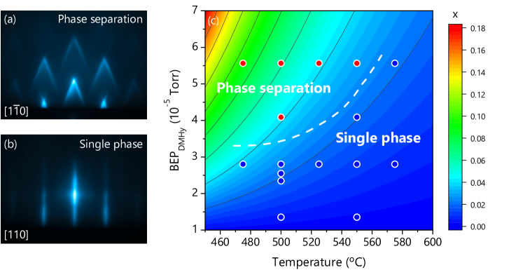
III.3 A growth diagram
All previous results are summarized here in a growth diagram that describes how the chemical and morphological properties of GaP1-xNx alloys grown by CBE depend on the growth parameters. Coming back to the control of the alloy composition, by combining Eqs. (1) and (4), the dependence of the N mole fraction on the growth temperature and the BEP values of the N and P precursors can be written in a compact form as:
| (5) |
where is a constant that might depend only on the impinging flux of the Ga precursor. By taking the mean values of and BEPth as 0.79 eV and Torr, we derived from the values of A and reported in section III.1 a value of for the Ga flux used in this study, i. e., 0.22 ML/s.
Figure 5(c) depicts a growth diagram, which visualizes according to Eq. (5) the impact of the growth temperature and BEPDMHy on the incorporation of N into GaP1-xNx. This diagram quantitatively holds for BEP Torr and the Ga flux used in this work. Nevertheless, analogous diagrams could be constructed for arbitrary values of BEPTBP using Eq. (5). Regarding the role of the actual Ga flux, it could affect the specific values of x, but we expect a comparable qualitative dependence of the N mole fraction on the growth temperature and BEPDMHy.
Besides the variation of x with the growth temperature and BEPDMHy, we also indicate in the growth diagram both the growth conditions of the samples grown in this study with BEP Torr (solid symbols), and the approximate boundary between the growth parameters resulting in single-phase and phase-separated GaP1-xNx layers (dashed line), as determined by the analysis of the samples by HRXRD. This boundary also applies to distinguish between growth conditions leading to flat and rough surface morphologies, as single-phase and phase-separated samples exhibit two- and three-dimensional RHEED patterns, respectively, as discussed above. The accuracy of our growth diagram was tested by comparing the N mole fractions shown in there with the actual ones measured by HRXRD for the samples prepared using the parameters indicated by the solid symbols shown in Fig. 5(c). The relative mean deviation between the expected and actual x values () is . The diagram thus provides a rather satisfactory description of x when considering all experimental uncertainties. Hence, Eq. (5) can be used to predict, with the aforementioned precision, the chemical composition of GaP1-xNx layers grown under unexplored growth conditions, at least for x values within the range analyzed here, i. e., .
To conclude, the growth diagram also evidences that identical chemical compositions can be achieved by combining different growth temperatures and BEPDMHy values, as these two parameters play opposite roles for the incorporation of N. It is also important to note that the phase-separated growth regime tends to extend towards lower values of x as thegrowth temperature is increased. Because of this effect and the exponential temperature dependence of x on the growth temperature, we recommend using moderate growth temperatures to prevent phase separation as well as to minimize the impact of possible temperature deviations on the final alloy composition. Nevertheless, it remains to be seen the impact of the growth temperature on point defects formation.
IV Summary and conclusions
We have comprehensively investigated the incorporation of N into GaP1-xNx layers grown on -oriented GaP-on-Si substrates by CBE using as gas sources DMHy, TBP and TEGa. According to our study, the N mole fraction: (i) exhibits an Arrhenius-like temperature dependence characterized by an apparent activation energy of eV, (ii) increases lineraly with the flux of DMHy, and (iii) is inversely proportional to the flux of TBP. The results are summarized in an empirical universal equation that can be used to predict the N mole fraction within the compositional range analyzed in this study, , with a relative degree of uncertainty of over the targeted value. All results are further illustrated in a growth diagram, which does not only visualize the dependence of x on the growth temperature and the flux of DMHy for given fluxes of TBP and TEGa, but also emphasizes under which growth conditions it is possible to obtain single-phase and flat GaP1-xNx layers. Importantly, although as a general trend chemical phase separation is triggered as the N mole fraction is increased, the threshold for the onset of phase separation is not just determined by x, it depends as well on the specific growth parameters. The maximum value of x we achieved for single-phase and flat GaP1-xNx layers was 0.039. This value is well above 0.021, i. e., the required N mole fraction for the synthesis of GaP1-xNx layers lattice matched to Si. This work thus evidences the feasibility of CBE for the monolithic integration of pseudomorphic GaP1-xNx-based optoelectronic devices on Si.
Data Availability Statement
The data that support the findings of this study are available from the corresponding author upon reasonable request.
Acknowledgements.
This work was supported by the former Ministerio de Ciencia, Innovación y Universidades and the current Ministerio de Ciencia e Innovación under Projects No. TEC2016-78433-R and PID2020-114280RB-I00, respectively. Additionally, S. Fernández-Garrido acknowledges the financial support received through the program Ramón y Cajal (co-financed by the European Social Fund) under Grant No. RYC-2016-19509 from Ministerio de Ciencia, Innovación y Universidades. We also thank to T. Vallés for his technical support and assistance.References
References
- [1] W Shan, K M Yu, W Walukiewicz, J Wu, J W Ager, and E E Haller. Band anticrossing in dilute nitrides. J. Phys.: Condens. Matter, 16:S3355, 2004.
- [2] J Chamings, S Ahmed, A R Adams, S J Sweeney, V A Odnoblyudov, C W Tu, B Kunert, and W Stolz. Band anti-crossing and carrier recombination in dilute nitride phosphide based lasers and light emitting diodes. Phys. Status Solidi B, 246:527, 2009.
- [3] H P Xin, R J Welty, and C W Tu. GaN0.011P0.989 red light-emitting diodes directly grown on GaP substrates. Appl. Phys. Lett., 77:1946, 2000.
- [4] C Cornet, C Robert, T N Thanh, W Guo, A Bondi, G Elias, A Létoublon, S Richard, J P Burin, M Perrin, J M Jancu, O Durand, J Even, S Loualiche, H Folliot, N Bertru, A Ponchet, and A L Corre. Carrier injection in GaAsPN/GaPN quantum wells on Silicon. IPRM 2011 - 23rd International Conference on Indium Phosphide and Related Materials, page 1, 2011.
- [5] C Robert, A Bondi, T N Thanh, J Even, C Cornet, O Durand, and J P Burin. Room temperature operation of GaAsPN/GaPN quantum well based light-emitting diodes: Effect of the incorporation of nitrogen. 251110:10, 2012.
- [6] N Jain and M K Hudait. III–V Multijunction Solar Cell Integration with Silicon: Present Status, Challenges and Future Outlook. Energy Harvesting and Systems, 1, 2014.
- [7] O Durand, S Almosni, Y Ping Wang, C Cornet, A Létoublon, C Robert, C Levallois, L Pedesseau, A Rolland, J Even, J M Jancu, N Bertru, A Le Corre, F Mandorlo, M Lemiti, P Rale, L Lombez, J.-F. Guillemoles, S Laribi, A Ponchet, and J Stodolna. Monolithic Integration of Diluted-Nitride III–V-N Compounds on Silicon Substrates: Toward the III–V/Si Concentrated Photovoltaics. Energy Harvesting and Systems, 1, 2014.
- [8] S Sukrittanon, R Liu, Y G Ro, J L Pan, K L Jungjohann, C W Tu, and S A Dayeh. Enhanced conversion efficiency in wide-bandgap GaNP solar cells. Appl. Phys. Lett., 107:153901, 2015.
- [9] K Kharel and A Freundlich. Band structure and absorption properties of (Ga,In)/(P,As,N) symmetric and asymmetric quantum wells and super-lattice structures: Towards lattice-matched III-V/Si tandem. J. Appl. Phys., 124:95104, 2018.
- [10] K Ben Saddik, A F Braña, N López, W Walukiewicz, and B J García. Growth of GaP1-x-yAsyNx on Si substrates by chemical beam epitaxy. J. Appl. Phys., 126:105704, 2019.
- [11] J Y Tsao, M H Crawford, M E Coltrin, A J Fischer, D D Koleske, G S Subramania, G T Wang, J J Wierer, and R F Karlicek. Solid-State Lighting: Toward Smart and Ultra-efficient Solid-State Lighting. Advanced Optical Materials, 2:803, 2014.
- [12] H Yonezu. Control of structural defects in group III – V – N alloys grown on Si. Semicond. Sci. Technol., 17:762, 2002.
- [13] S Almosni, C Robert, T Nguyen T., C Cornet, A Létoublon, T Quinci, C Levallois, M Perrin, J Kuyyalil, L Pedesseau, A Balocchi, P Barate, J Even, J M Jancu, N Bertru, X Marie, O Durand, and A Le Corre. Evaluation of InGaPN and GaAsPN materials lattice-matched to Si for multi-junction solar cells. J. Appl. Phys., 113:123509, 2013.
- [14] J.-M. Tilli, H Jussila, K M Yu, T Huhtio, and M Sopanen. Composition determination of quaternary GaAsPN layers from single X-ray diffraction measurement of quasi-forbidden (002) reflection. J. Appl. Phys., 115:203102, 2014.
- [15] K Yamane, S Mugikura, S Tanaka, M Goto, H Sekiguchi, H Okada, and A Wakahara. Impact of temperature and nitrogen composition on the growth of GaAsPN alloys. J. Cryst. Growth, 486:24, 2018.
- [16] M A G Balanta, P B A de Oliveira, H Albalawi, Y Galvão Gobato, H V A Galeti, A D Rodrigues, M Henini, S Almosni, C Robert, A Balocchi, Y Léger, H Carrère, M Bahri, G Patriarche, X Marie, and C Cornet. Effects of nitrogen incorporation and thermal annealing on the optical and spin properties of GaPN dilute nitride alloys. J. Alloys Compd., 814:152233, 2020.
- [17] S Nagarajan, H Jussila, J Lemettinen, K Banerjee, M Sopanen, and H Lipsanen. Strain-compensated GaPN/GaP heterostructure on (001) silicon substrates for intermediate band solar cells. J. Phys. D: Appl. Phys., 46:165103, 2013.
- [18] Q Li and Kei M Lau. Epitaxial growth of highly mismatched III-V materials on (001) silicon for electronics and optoelectronics. Prog. Cryst. Growth Charact. Mater., 63:105, 2017.
- [19] Y.-M. Houng. Chemical beam epitaxy. Crit. Rev. Solid State Mater. Sci., 17:277, 1992.
- [20] J Miguel-Sánchez, A Guzmán, and E Muñoz. Role of N ions in the optical and morphological properties of InGaAsN quantum wells for 1.3–1.5 m applications. Appl. Phys. Lett., 85:1940, 2004.
- [21] A Utsumi, H Yonezu, Y Furukawa, K Momose, and K Kuroki. Increase in luminescence efficiency of GaPN layers by thermal annealing. Phys. Status Solidi C, 0:2741, 2003.
- [22] S Y Moon, A Utsumi, H Yonezu, Y Furukawa, T Ikeda, and A Wakahara. GaPN-GaP double heterostructure light emitting diode grown on GaP substrate by solid-source molecular beam epitaxy. Phys. Status Solidi A, 201:2695, 2004.
- [23] N Y Li, W S Wong, D H Tomich, H K Dong, J S Solomon, J T Grant, and C W Tu. Growth study of chemical beam epitaxy of GaNxP1-x using NH3 and tertiarybutylphosphine. J. Cryst. Growth, 164:180, 1996.
- [24] I Suemune, T Shimozawa, K Uesugi, H Kumano, H Machida, and N Shimoyama. Metalorganic Molecular-Beam Epitaxial Growth and Optical Properties of Er-Doped GaNP. Jpn. J. Appl. Phys., 41:1030, 2002.
- [25] M Ait-Lhouss, J L Castaño, and J Piqueras. Chemical beam epitaxial growth of GaAs from tertiarybutylarsine and triethylgallium precursors. Mater. Sci. Eng. B, 28:155, 1994.
- [26] Tobias Roesener, Vera Klinger, Christoph Weuffen, David Lackner, and Frank Dimroth. Determination of heteroepitaxial layer relaxation at growth temperature from room temperature X-ray reciprocal space maps. J. Cryst. Growth, 368:21, 2013.
- [27] J.-M. Chauveau, Y Androussi, A Lefebvre, J Di Persio, and Y Cordier. Indium content measurements in metamorphic high electron mobility transistor structures by combination of x-ray reciprocal space mapping and transmission electron microscopy. J. Appl. Phys., 93:4219, 2003.
- [28] Yasufumi Takagi, Yuzo Furukawa, Akihiro Wakahara, and Hirofumi Kan. Lattice relaxation process and crystallographic tilt in GaP layers grown on misoriented Si(001) substrates by metalorganic vapor phase epitaxy. J. Appl. Phys., 107:63506, 2010.
- [29] I Vurgaftman, J R Meyer, and L R Ram-Mohan. Band parameters for III–V compound semiconductors and their alloys. J. Appl. Phys., 89(11):5815, 2001.
- [30] W G Bi and C W Tu. N incorporation in GaP and band gap bowing of GaNxP1-x. Appl. Phys. Lett., 69:3710, 1996.
- [31] B Kunert, J Koch, T Torunski, K Volz, and W Stolz. MOVPE growth experiments of the novel (GaIn)(NP)/GaP material system. J. Cryst. Growth, 272:753, 2004.
- [32] A Wakahara, Y Furukawa, S Itoh, S Hatakenaka, and H Yonezu. Growth and characterization of GaPN by OMVPE. J. Cryst. Growth, 300:182, 2007.
- [33] K Onabe. MOVPE Growth and Optical Characterization of GaPN Metastable Alloy Semiconductor. MRS Proc., 449:23, 1996.
- [34] H Suzuki, K Nishimura, H S Lee, Y Ohshita, N Kojima, and M Yamaguchi. Carbon incorporation process in GaAsN films grown by chemical beam epitaxy using MMHy or DMHy as the N source. Thin Solid Films, 515:5008, 2007.
- [35] D Wildt, B J García, J L Castaño, and J Piqueras. Phosphorus and arsenic incorporation during chemical beam epitaxial growth of strained GaAs1-xPx layers on GaAs(100) substrates. Proceedings of the 10th Conference on Semiconducting and Insulating Materials (SIMC-X) (Cat. No.98CH36159), IEEE, page 15, 1999.
- [36] T. J. Grassman, M. R. Brenner, S. Rajagopalan, R. Unocic, R. Dehoff, M. Mills, H. Fraser, and S. A. Ringel. Control and elimination of nucleation-related defects in GaP/Si(001) heteroepitaxy. App. Phys. Lett., 94(23):232106, 2009.