Gain and Pain of a Reliable Delay Model
jmaier@ecs.tuwien.ac.at
Abstract
State-of-the-art digital circuit design tools almost exclusively rely on pure and inertial delay for timing simulations. While these provide reasonable estimations at very low execution time in the average case, their ability to cover complex signal traces is limited. Research has provided the dynamic Involution Delay Model (IDM) as a promising alternative, which was shown (i) to depict reality more closely and recently (ii) to be compatible with modern simulation suites. In this paper we complement these encouraging results by experimentally exploring the behavioral coverage for more advanced circuits.
In detail we apply the IDM to three simple circuits (a combinatorial loop, an SR latch and an adder), interpret the delivered results and evaluate the overhead in realistic settings. Comparisons to digital (inertial delay) and analog (SPICE) simulations reveal, that the IDM delivers very fine-grained results, which match analog simulations very closely. Moreover, severe shortcomings of inertial delay become apparent in our simulations, as it fails to depict a range of malicious behaviors. Overall the Involution Delay Model hence represents a viable upgrade to the available delay models in modern digital timing simulation tools.
Index Terms:
Circuit models, glitch propagation, dynamic delay models, pulse degradation, faithful digital timing simulation, metastability analysisI Introduction
Modern circuit designs dedicate a major share of the overall development time to verification, in particular to answer questions like: At which pace propagate signals through the logic? How does their appearance change on their path? Can they be properly sampled at the output by succeeding units? To answer them simulations are heavily utilized.
The most accurate methods currently available to determine the behavior of a circuit are analog simulation suites like SPICE. These calculate time- and value-continuous signal traces based on very elaborate physical models. This is, however, a computationally expensive task such that analyses of larger circuits quickly exceed reasonable execution times.
To reduce the overall complexity, simulations are, in general, executed in the digital domain, where the analog trace are abstracted by zero time transitions between the discrete values LO and HI. Determining the temporal evolution of digital signals throughout the circuit is done in various fashions: The static timing analysis (STA) solely considers the static delay of a single input transition. Deriving reasonable values for a rising and falling transition is quite challenging, since they depend on a lot of parameters and thus differ among gates. For this purpose extensive analog simulations are carried out in advance, which then serve as basis for proper predictions. Prominent examples are the Extended Current Source Model (ECSM) by Cadence® [1] or the Complex Current Source Model (CCSM) by Synopsys® [2].
STAs are well suited to determine, for example, the maximum clock frequency. However, other effects, like signal degradation or interference that may result in very short pulses, cannot be identified. For this purpose dynamic timing simulations, which predict time and direction of a gate’s output transitions based on time and direction of its input transitions, are mandatory. Although several approaches are currently available (see Section II), Függer et al. [3] revealed, that solely the Involution Delay Model (IDM) is able to predict the behavior of a circuit solving the short pulse filtration problem. Recently Öhlinger et al. [4] practically applied the IDM to basic circuits, however, primarily to evaluate the accuracy of their introduced simulation framework. Consequently little is known about the behavioral coverage and performance of the IDM in realistic setups.
Main contributions: In this paper we are thus extending the evaluation of the IDM to additional place & routed circuits: For an OR Loop, an SR Latch and a ripple-carry Adder (i) analog and digital simulations are run, (ii) the achieved results are evaluated and finally (iii) the introduced overhead is determined. Our analyses (1) confirm the simple applicability of the IDM stated in [4], (2) show a high correlation between IDM and analog simulation results and (3) reveal major shortcomings of the approaches that are currently in use. The realistic behavioral description, however, also leads to a significant overhead in the simulation time of up to %.
This paper is organized as follows: In Section II we provide a short introduction to existing delay models, first and foremost to the IDM and its fundamental properties. Section III then contains a description of the simulation setup and the investigated circuits. A discussion of the achieved IDM results and the shortcomings of inertial delay together with an evaluation of the introduced overhead follows in Section IV. Finally, we conclude the paper in Section V.
II Background
In this section we want to provide a short overview over existing delay prediction methods, whereat we will focus in greater detail on the basics of the Involution Delay Model (IDM). For more details the interested reader is referred to the original publication [3].
The most straight-forward approach for digital delay estimation is clearly the pure delay which introduces a retardation of resp. . Obviously this leads to a linear relationship between input () and output () pulse width, i.e., the time difference between transitions of opposite directions. Fig. 1 shows the relationships for up-pulses (falling after rising transition) and down-pulses (falling before rising). The also depicted inertial delay is very similar, with the difference that pulses below a certain threshold are not propagated. Although a comparable behavior is observable in analog SPICE simulations, they mainly differ by a gradual degradation of . Capturing this effect is mandatory to realistically model the generation of glitches, i.e., very short pulses. Juan-Chico et al. [5] showed that inertial delay is unfit for this task which lead to the development of the Degradation Delay Model (DDM) [6]. This approach predicts the delay value using nonconstant delay functions resp. . The parameter is thereby defined as the time span from the last output transition to the current input transition, as is shown in Fig. 2.
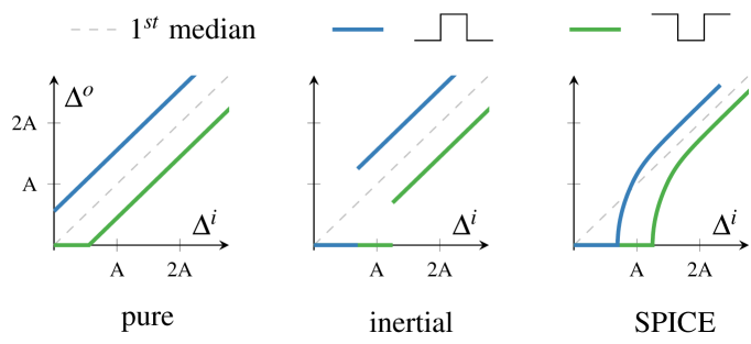
For long input pulses (large values of ), can be assumed to be constant, comparable to inertial/pure delay. Decreasing the pulse width eventually leads to a decline of , cp. Fig. 1, and hence to significant degradation. Finally, the equilibrium point is reached, which generates a zero-time glitch at the output. For even shorter input pulses the model schedules the digital output transitions in the wrong temporal order, e.g., when starting at LO a falling before a rising transition. In this case we speak of cancellation and both transition are removed. In the analog domain this corresponds to sub-threshold trajectories.
Despite its removal during cancellation, the latest transition time is still crucial, as it serves as reference point for the calculation of the succeeding . Since there are no more threshold crossings at the output available, that could be used to determine the delay, has to be predicted. For this purpose DDM simply extends the fitting of derived for . While this seems, at a first glance, like a legitimate choice it causes the delay estimation to fail in certain circumstances. In detail Függer et al. [8] were able to prove that all existing approaches, including DDM, pure and inertial delay, cannot faithfully model a circuit that solves the short-pulse filtration problem (SPF). In consequence the Involution Delay Model [3] was developed, with the distinguishing property that input pulses with have diminishing effect on the output. An interpretation of the model in the analog domain is described by the authors in the following fashion: The digital input signal first passes a pure delay component and is then transformed to the analog domain using two unique waveforms ( from LO to HI, from HI to LO), which are switched instantaneously upon a transition. Finally the analog trajectory is fed into a comparator, which issues a digital output event whenever the threshold voltage is crossed.
Although DDM and especially IDM have much higher expressive power modern circuit designs still heavily rely on the simple pure and inertial delay models. This is not surprising, given the very good integration in state-of-the-art simulation suites and thus its simple applicability: Implementations based on popular hardware description languages like VHDL Vital [9] or Verilog [10] are widespread. Albeit there is a distinguished simulation tool for DDM [11] available, it is shipped as a separate executable, making it demanding to integrate the simulation into an existing design flow. To circumvent this problem for the IDM, Öhlinger et al. [4] developed the InvTool, whose VHDL procedures simply have to be linked and thus enforce no changes on the established work flow.
III Experimental setup
To determine the behavioral coverage and performance of the IDM we chose to run analog and digital simulations. The respective framework, which utilizes the Nangate Open Cell Library with FreePDK15 FinFET models [12] (), is described in the sequel. A presentation and evaluation of the results follows in Section IV. The simulation data is freely available on-line111https://github.com/jmaier0/idm_evaluation.
III-A Design Flow
For the sake of realistic results we utilize the Cadence® tools GenusTM and InnovusTM (version 19.11) to place & route the design and automatically extract the parasitics (.spef format) and static delay values (.sdf format). For analog transient simulations we back-annotate the extracted parasitics to a transistor level model, which is then executed using Cadence® Spectre® (version 19.1). Note that these results serve as golden reference for the digital predictions, which enables a quick and simple evaluation regarding the correctness and behavioral coverage.
The digital simulations are run with Mentor® ModelSim® (version 10.5c), which reads the .sdf file to parameterize the circuit netlist generated by InnovusTM. Two prediction approaches were executed: The default one provided by the tool (INE), essentially an inertial delay, and the Involution Delay Model (IDM). For the latter we used the InvTool222https://github.com/oehlinscher/InvolutionTool, to retrieve the desired -channel model (ea/p_exp_channel.vhd). Note that the XOR gate could not be generated automatically and had to be created manually. Since the .sdf file just defines the static delays , we set, for the sake of simplicity, the pure delay to a constant value of .
We want to emphasize at this point that we were able to confirm the simplicity of applying IDM to an existing design flow. Starting from the test setup for INE we solely had to compile and link the respective IDM files. Nevertheless, we were not able to reuse our testbench since the IDM and the tool’s delay model are implemented in differing hardware description languages (Verilog vs. VHDL). Some commands, such as forcing signals, do not properly work across language boundaries, which made it necessary to duplicate the testbench while, of course, conserving the same behavior.
III-B Circuits
In the sequel we introduce the circuits used in our simulations. Note that additional buffers, which we added at the in- and output to emulate the settings far away from the chip boundaries, are not shown.
III-B1 OR Loop
In its bare form the circuit shown in Fig. 3 has been used in [3] for proofing the faithfulness of IDM regarding the SPF problem. It utilizes an arbitrary amount of buffers to create a combinatorial loop, whereat up-pulses are coupled in via a single OR-gate. Based on the input pulse width the signal may oscillate for a possibly infinite amount of time before vanishing or setting the loop to HI. Depending on the length of the feedback path either distinguished pulses or intermediate voltage values are observable. While the former corresponds to a simple ring oscillator the latter depicts metastability [13], which leads to a wide range of problematic behaviors such as late output transitions or a spurious mapping to LO and HI among succeeding gates. Thus it is crucial to model metastable upsets in a suitable fashion in the digital domain. To ease the descriptions of oscillations and metastability we are going to use and to denote the high respectively low time of the oscillation at node A.
To focus on different characteristics we ran simulations with a varying number of buffers in the feedback path, which effectively varies the loop delay. We are aware that the same could also be achieved by adding capacitances, however, in our setup this would lead to significantly different results since a capacitance serves as a low pass filter and thus suppresses short, high frequency, pulses very effectively. Using multiple buffers in succession, on the contrary, conserves the signal shape such that oscillating signals can be generated. Nonetheless we artificially added a large capacitance at node B, which enables us (i) to analyze the internal behavior and (ii) to reveal shortcomings of the delay models more easily.
III-B2 SR Latch
The second circuit we chose is the SR Latch as shown in Fig. 4, a well-known circuit with the possibility for metastability and slightly improved complexity. Note that we added a single buffer on the coupling paths between the NOR-gates, to pronounce the observable effects and thus ease their detection.
The Set Reset Latch operates very intuitively: If the set () input turns HI, switches to HI, for a HI on the reset () input, changes to LO. represents the inverse of and thus shows the opposite behavior. Both inputs set to HI leads to an intermediate voltage value at nodes U & T and thus has to be prevented. Note the similarities between SR Latch and OR Loop: If one input is LO, the SR Latch behaves, w.r.t. the other one, just like the OR Loop: Very short pulses are blocked, very long ones immediately set the loop, while ones in between may lead to metastability. Significantly different behavior is possible, however, if both inputs are allowed to change. While one steers the loop into a metastable state the other one can either support or impair its resolution, a fact that we will exploit in our simulations.
III-B3 Adder
To investigate the scaling of the IDM and its predictions on loop-free circuits we also simulated a simple ripple carry adder as shown in Fig. 5, whereat we used . Each full adder block FA is defined on the gate level and implements the equations
Out of the manifold input possibilities, those leading to a maximum number of transitions are the most interesting for our analysis, as they allow an investigation of the whole circuit in a single simulation run. For this purpose we chose , and introduced an up-pulse on signal . For a down-pulse on signal we used a very similar setup, with the sole difference of setting initially.
IV Results
In this section we present and compare the analog resp. digital simulation results for the circuits introduced in Section III. We start by studying oscillatory behavior and its digital counterpart for the OR Loop with long feedback delay. Subsequently we remove the buffers from the feedback path and investigate the effects on the (significantly changing) analog and (only slightly differing) digital simulation results. Afterwards we use the SR Latch to demonstrate the superior modeling power of the IDM, which, in contrast to inertial delay, predicts the metastable behavior quite well. Simulations of the Adder confirm the superiority of the IDM but also reveal inaccuracies. Finally we present an extensive comparison of the overhead and thus the price that has to be paid.
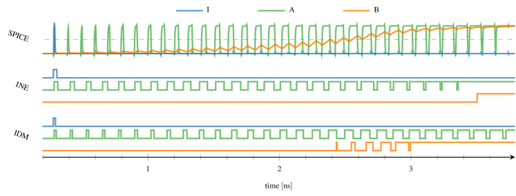
IV-A OR Loop with Long Feedback
For our first experiments we added thirty buffers to the feedback path. In this setup it is, for , possible to generate multiple periodic signals in the loop since the signal rise/fall time is significantly smaller than the overall delay of the loop. However, the static delay values extracted after place & route did not match: Rising transitions are delayed less than falling ones, leaving exactly one that perfectly compensates the increase in by pulse degradation effects and thus creates infinite oscillation.
IV-A1 SPICE
Fig. 6 (top) shows the analog simulation results for an initially very short pulse that grows and eventually settles the loop at . Clearly visible is the impact of the high capacitive load. Since the transitions at node A are very quick compared to node B it actually seems as if charging and discharging curves are switched immediately when an input transition occurs333Recall that this perfectly matches the analog domain model of the IDM. Consequently the threshold (dashed line) is crossed multiple times, whereat the time difference between rising and falling trajectories strictly increases.
Noteworthy is the high sensitivity of the feedback loop in this operation region and thus also the very low probability to reach such a state. We had to vary in steps of in order to eventually generate an oscillation trace inside the loop that lasted at most .
IV-A2 INE
At a first glance the inertial delay results shown in Fig. 6 (middle) look comparable. The short initial pulse increases until the loop is constant HI and thus also node B gets HI. However, on closer examination a severe shortcoming is revealed: The shown pulse is the shortest one that can be inserted into the loop, as smaller ones are removed by a high-delay buffer at the input. This indicates a general problem: A gate with long delay at the front may remove a big share of the input pulses, which can include highly relevant ones. Consequently it is impossible to detect any infinite or decaying oscillations for the shown circuit using INE.
Note that the rising transition at node B only occurs after the loop has fully settled, i.e., the oscillations have ceased. This can again be explained by the big delay of the succeeding gate, which thus serves as a metastability filter. This does, however, not correspond well to the analog simulations, where the threshold is already crossed way before the loop is fully locked. Therefore INE is not suited to properly describe the exact behavior of the circuit in such circumstances. In particular, it is impossible to achieve pulses at node B for the inertial delay model: only a single transition is observed or none at all.
IV-A3 IDM
Compared to INE the Involution Delay Model achieves a much more fine grained behavioral description. First and foremost, any value of can be generated, also ones that quickly decay. Fig. 6 (bottom) shows a simulation with increasing for ascending : Considering the model representation in the analog domain presented in Section II this corresponds to utilizing for an increasing and for a decreasing amount. Consequently the mean analog value steadily rises, eventually crossing and resulting in the digital oscillations on node B shown in the figure.
By properly tuning it is even possible to achieve an infinite pulse train, i.e., one that perfectly recreates itself. Note that, although the loop is highly unstable in this configuration, not a single transition on B could be observed, which reveals a problem of the IDM: Depending on the value of the discretization threshold voltage , zero, one or infinitely many transitions are indicated for the same analog trajectory.
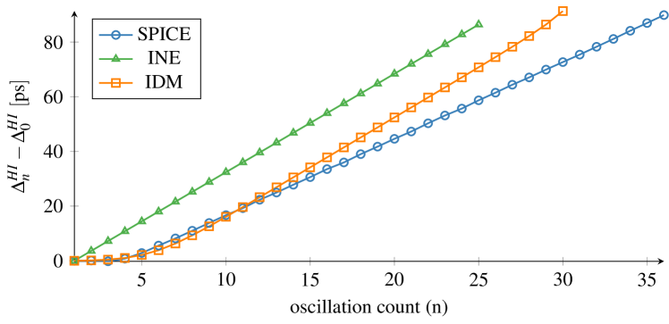
IV-A4 Comparison
IDM and INE also handle the evolution of , shown in Fig. 7, differently. Consider that the rate of growth is determined as the gap between falling and rising transition delay, which is constant for INE due to fixed delay values. Consequently a linear increase of can be observed. SPICE and IDM, however, show a quite different behavior: For small , increases only marginally, as the circuit initially operates near the metastable point, i.e., where pulses recreate themselves. With increasing pulse width the rate, however, quickly ramps up.
Very interesting is the nonlinear increase of the IDM. Intuitively, is expected to settle at a constant rate, since for large values of the IDM and inertial delay are equal. While this is true, one has to consider that the increase in causes a drop of , which eventually experiences pulse width degradation and thus further enhances the increase rate of .
IV-B OR Loop with Direct Feedback
Recall that the buffer count in the feedback path is a very sensitive parameter with major implications: Reducing the delay of the loop moves rising and falling transitions closer together, while leaving the rise and fall time untouched. Eventually the single transitions will merge meaning that GND/ are not reached any more.
The effects on the infinite oscillatory behavior are as follows: As long as there is at least one gate in the loop still performing full range switching, which is possible due to differing parasitics, oscillations with a reduced amplitude, i.e., within the range with and , are possible (cf. Section IV-C). Due to the lower amplitude, the time between succeeding threshold crossings declines and thus the oscillation frequency increases. Further reducing the delay finally leads to a damped oscillation, whereat the damping factor is increased with decreasing delay. For the simulations presented in the sequel we removed all gates and thus force a direct transition to the constant metastable voltage.
IV-B1 SPICE
Analog simulations confirm our intuitive explanation. Fig. 8 shows two traces on node A, which stay at a constant value near for some time and then resolve to LO in one case and to HI in the other one. The facts that the corresponding only differ by and, nonetheless, it is only possible to stay in the metastable state for a few picoseconds, indicate the very high sensitivity of this circuit configuration.
IV-B2 INE
As described in Section IV-A the shaping gates at the input filter many incoming pulses. In fact, only those longer than the delay of the storage loop are able to pass, causing an immediate switch to HI. Consequently, for INE, the simulation either delivers a single rising transition on all wires or none at all. While this might seem reasonable at a first glance, the metastable state, and thus the increase in delay, are not revealed, suggesting falsely a settled and well defined behavior.
IV-B3 IDM
Although the analog simulations did not show any crossing during metastability, the IDM again delivers an oscillatory behavior, which seems to be awfully wrong. Considering, however, the analog representation, more specifically the switching between and , it becomes apparent that the closest the analog trajectory in the IDM can get to a constant intermediate value is to oscillate around it. Therefore a pulse train is used to indicate metastability.
The fact that the IDM used a pulse train to describe both real oscillations in Section IV-A as well as metastability begs the question: How can these scenarios be distinguished? The answer is discouraging. Solely based on the digital predictions this is impossible. The major difference among oscillatory traces are respectively , which, however, do not yield much information on their own. Only in combination with the switching waveforms & or the static delays it is possible to estimate the voltage gain during the HI resp. LO period. As s rule of thumb one has to expect damping if () is approximately or lower than ().
In our setup we extracted and for the OR-gate, which is clearly more than respectively in Fig. 8. Although this seems very disadvantageous for the IDM be advised that also for INE comparisons with the delay values are necessary to determine if a pulse is close to suppression. Since knowing the peak values in the analog domain is so important we are currently working on an extension of the IDM that is able to indicate the underlying analog waveform. This is, however, only suited for rough estimations and is not intended to replace analog simulations.
Overall it has to be stated that an oscillating simulation trace does not automatically indicate an undesired behavior. Just as periods reach a circuit dependent range ill shaped pulses or even metastability have to be inferred.
IV-C SR Latch
After studying the general behavior of digital simulation approaches on the rather synthetic OR Loop, we now turn to the common SR Latch. Interestingly, INE again fails to cover very important parts of the real behavior and thus delivers overly optimistic results, while the IDM stays close to the analog trace. The latter even enables us to explore unfavorable input conditions, which we will use to artificially prolong metastability.
IV-C1 Set or Reset Input Pulse
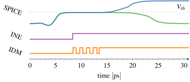
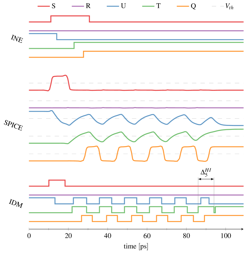
Since setting either or LO degrades the SR Latch to the OR Loop w.r.t. the other input, simulations shown in Fig. 9 lead to similar results. For INE the shortest pulse, that is able to pass the input buffers, once again immediately sets the loop, leading to a single output transition. This strongly contradicts the analog simulation, which shows (non full-range) oscillations on all wires. As discussed earlier, such a behavior is possible if one of the gates in the path, in this case the buffers, still issue full range waveforms.
In contrast, the IDM describes the behavior in, and also the resolution out of, metastability faithfully, which enabled us to search for “malicious” input conditions that prolong the metastable state. In Fig. 9 a very long HI phase () on node T is visible as Q switches to constant HI. To prevent the oscillation from resolving it would be necessary to decrease and simultaneously increase . Reiher et al. [14] described a similar effect when “kicking” synchronizers, i.e., abruptly changing an internal voltage value, which also led to a potential extension of the metastable state.
It can be easily retraced that a properly placed up-pulse on the reset input does the trick. Essential for success is the time of the rising transition, as it determines the width of . On the contrary the falling transition can be issued at any point in time during the HI period of the other NOR-gate input, since in this case the reset input is masked anyway.
IV-C2 Set and Reset Input Pulse
To verify our predictions, we extended the previous simulation by a pulse on input . Results for INE, shown in Fig. 10 (top), reveal solely one additional output transition and thus suggest a fully settled circuit, while completely hiding the potential instabilities.
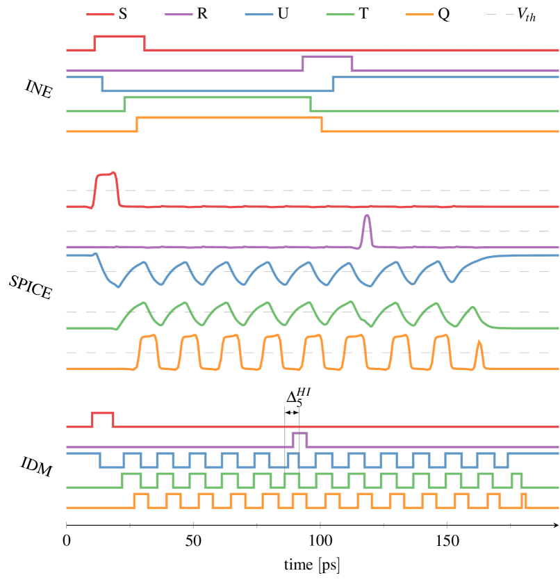
On the contrary, SPICE simulations shown in Fig. 10 (middle) confirm our predictions. Not only is metastability extended but also a resolution to HI is forced. We want to emphasize that the signal on used to prolong metastability is too short to have any impact on a fully settled memory loop, which was revealed by further simulations. Only in combination with this particular unstable circuit state a change in value becomes possible. Consequently, a close observation of unstable states and short pulses is very important.
Finally an execution of the IDM shown in Fig. 10 (bottom) delivers exactly the predicted behavior. Cutting indeed sets the loop back into metastability, resulting in a very realistic representation of the underlying analog behavior.
IV-D Adder
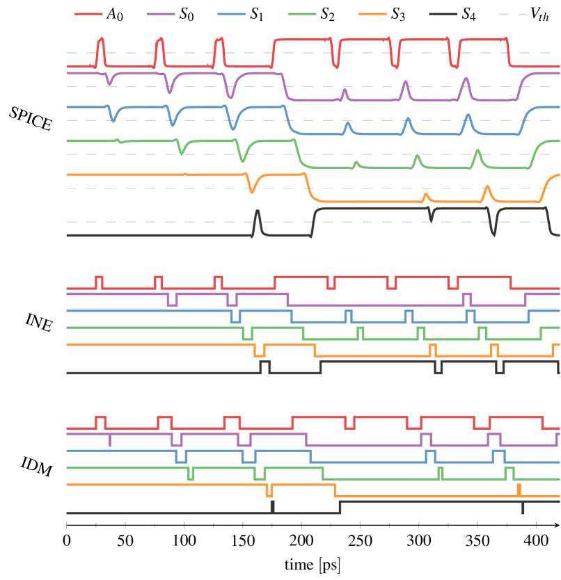
At last we turn to the four Bit Adder to evaluate the scaling potential of the IDM. Analog SPICE simulation results [see Fig. 11 (top)] clearly show the propagation of the input pulse through the unit and the corresponding degradation. Whether a pulse is observed on output depends on (i) the initial input pulse width on signal and (ii) the path length from to . The longer the path the bigger the input signal has to be to still have an impact. Interestingly the carry signals seem to be faster than the ones representing the corresponding sum value , which can be seen very clearly by comparing and (the latter is actually the carry signal of the last full adder). While still barely crosses the threshold already reaches all the way to GND/.
Overall these results show the threat caused by glitches: Due to the differing path lengths through the circuit the input signal generates a varying number of output pulses with decreasing pulse widths on signals which elevate the chance to violate the setup and hold times of succeeding flip-flops. Furthermore we want to emphasize that in this circuit a metastable input value has the chance to spread to five output signals and thus the effect of a single upset gets multiplied. This shows, once more, the importance of faithfully predicting glitches and metastability in the first place.
For INE a very inconsistent buildup of transitions can be observed: Increasing the pulse width of an input, that only induced a pulse on , by , caused a pulse propagation all the way up to . This is a direct consequence of the fact, that INE suppresses pulse widths below a certain threshold, as was shown in Fig. 1. For down-pulses on INE even delivers very nonphysical results as signal only starts to change after every other signal had been triggered. We retraced this to an unfortunate series of delays causing the signal closest to the input switch last, which is the actual opposite of what is seen in analog simulations. Finally note the constant shifts in pulse widths, i.e., once a pulse appears on a signal its pulse width differs from the input pulse solely by a constant additive value. These values are very similar for each output such that very similar output traces are achieved.
A smooth increase of pulse widths is naturally much better modeled by the IDM. In the simulations we even observed a strict causality among to , i.e, showed a transition after all had also switched. Compared to INE this is a big improvement. Compared to SPICE, however, some inaccuracies are still observable. For example the quick increase on in relation to is not well depicted. Possible causes are inaccurate delay values extracted from the design (as reported in [4]) or the still nonoptimal description of multi-input gates. Nonetheless, due to its accurate pulse width degradation coverage, the IDM is able to provide overall realistic results.
| INE | IDM | ||||
|---|---|---|---|---|---|
| # | [] | [] | [] | [] | overhead [%] |
IV-E Overhead
Calculating delay values for the IDM, which includes exponential and logarithmic operations, is obviously computationally more expensive than applying constant values paired with some minor removal checks for INE. To evaluate the overhead we ran extensive simulations and measured the execution time (Intel Xeon X5650, 1600 MHz, 32 GB RAM, CentOS 6.10). As test circuits we chose to use the Adder and the Clock Tree of an open source MIPS processor [15] that comprises of inverters which drive flip-flops. To also generate results for larger circuits we simply instantiated each unit multiple times.
For comparable results we had to ensure that INE and the IDM process the same amount of transitions. Since their behavior mainly differs for high input frequencies we used rather long pulses to assure no internal cancellations, whereat overall input transitions were applied per simulation run. The results are shown in Table I for the Adder and in Table II for the Clock Tree, whereat the first column denotes how often the circuit had been instantiated. First and foremost we want to note that due to a rather high variance we ran each simulation times and calculated the average respectively . Furthermore be advised that the presented values serve as lower bound, since real input signals may lead to very short internal pulses which increases the workload of IDM compared to INE.
In essence the results show that the improved coverage of the IDM definitely comes at a price. For the Adder the overhead increases with circuit size, while for instances it is almost %. The significant elevated values for and instances show a bottleneck of the computational platform that is not experienced by both methods in the same fashion, making them not representative. For the Clock Tree the overhead is lower and more constant, ranging from to almost %. We explain the deviation by the fact that only simple inverters are utilized, again showing that there is still a lot to be done in the IDM regarding multi-input gates.
| INE | IDM | ||||
|---|---|---|---|---|---|
| # | [] | [] | [] | [] | overhead [%] |
IV-F Summary
Our simulation results have shown that INE fails to model wide ranges of undesired behaviors in the form of high frequency oscillations or metastable intermediate voltages. The causes are single gates with larger delays, which have to be expected in almost every real world circuit. Relying exclusively on these predictions thus leads to a false sense of security. Investing sometimes considerably more computational effort by applying the IDM leads to a much better behavioral coverage and, in consequence, more trustworthy results. We therefore claim that the Involution Delay Model is able to enhance digital simulations significantly.
V Conclusion and Future Work
In this paper we evaluated the Involution Delay Model (IDM), an elaborate alternative to classic digital timing analysis approaches. To motivate this statement we ran analog (SPICE) and digital (inertial delay, IDM) simulations on three different circuits (simple OR-loop, an SR-latch and an adder) and compared the derived results. Appropriate interpretation of the predictions by the IDM confirmed the high behavioral coverage, especially for short pulses. On the contrary a single high delay gate, which blocks a large share of incoming pulses, caused massive mispredictions for inertial delay. Consequently state-of-the-art simulation suites tend to miss potentially malicious circuit states like infinite oscillations or metastability. Although an evaluation of the overhead introduced by the IDM showed a significant increase in simulation time, we still think that the IDM poses a viable alternative to existing approaches, especially if confined to the most critical parts.
In the paper we argued, that a proper interpretation of the digital results, i.e., whether a signal shows malicious behavior, is only possible by considering the internal analog representation. Thus, future work will be devoted to developing an extension that allows the designer to take a look at the underlying analog traces on top of the digital results. Furthermore, we are considering ways to improve the coverage of metastable behavior that is currently not detectable at the digital output and of course performance improvements.
One point deliberately neglected in this paper is accuracy. Investigations by Öhlinger et al. [4] and Maier et al. [7] revealed that deriving appropriate description is a nontrivial task. Furthermore, characterizing each single gate by relying heavily on analog simulations is computationally expensive. Approaches that yield reasonable results based on available, or easily achievable, data are instrumental for making the IDM a truly competitive alternative to existing delay models.
References
- [1] Effective Current Source Model (ECSM) Timing and Power Specification, Cadence Design Systems, January 2015, version 2.1.2.
- [2] CCS Timing Library Characterization Guidelines, Synopsis Inc., October 2016, version 3.4.
- [3] M. Függer, R. Najvirt, T. Nowak, and U. Schmid, “A faithful binary circuit model,” IEEE Transactions on Computer-Aided Design of Integrated Circuits and Systems, August 2019.
- [4] D. Öhlinger, J. Maier, M. Függer, and U. Schmid, “The involution tool for accurate digital timing and power analysis,” Integration, vol. 76, pp. 87 – 98, 2021. [Online]. Available: http://www.sciencedirect.com/science/article/pii/S0167926020302777
- [5] J. Juan-Chico, P. Ruiz de Clavijo, M. J. Bellido, A. J. Acosta, and M. Valenia, “Inertial and degradation delay model for cmos logic gates,” in 2000 IEEE International Symposium on Circuits and Systems (ISCAS), vol. 1, 2000, pp. 459–462 vol.1.
- [6] M. J. Bellido, J. Juan, and M. Valencia, Logic-Timing Simulation and the Degradation Delay Model. Imperial College, 2005. [Online]. Available: https://www.worldscientific.com/doi/abs/10.1142/p411
- [7] J. Maier, M. Függer, T. Nowak, and U. Schmid, “Transistor-level analysis of dynamic delay models,” in 2019 25th IEEE International Symposium on Asynchronous Circuits and Systems (ASYNC), 2019, pp. 76–85.
- [8] M. Függer, T. Nowak, and U. Schmid, “Unfaithful glitch propagation in existing binary circuit models,” in Proceedings of the 19th IEEE International Symposium on Asynchronous Circuits and Systems (ASYNC). New York City: IEEE Press, 2013, pp. 191–199.
- [9] IEEE Standard for VITAL ASIC (Application Specific Integrated Circuit) Modeling Specification, IEEE Computer Society, Sep. 2001, IEEE Std 1076.4-2000.
- [10] IEEE Standard Verilog Hardware Description Language, IEEE Computer Society, Sep. 2001, IEEE Std 1264-2001.
- [11] P. Ruiz de Clavijo Vazquez, J. Juan-Chico, M. J. Bellido, A. Acosta, and M. Valencia, “Halotis: High accuracy logic timing simulator with inertial and degradation delay model,” in Proceedings Design, Automation and Test in Europe. Conference and Exhibition 2001, 2001, pp. 467–471.
- [12] M. Martins, J. M. Matos, R. P. Ribas, A. Reis, G. Schlinker, L. Rech, and J. Michelsen, “Open cell library in 15nm freepdk technology,” in Proceedings of the 2015 Symposium on International Symposium on Physical Design, ser. ISPD ’15. New York, NY, USA: ACM, 2015, pp. 171–178. [Online]. Available: http://doi.acm.org/10.1145/2717764.2717783
- [13] R. Ginosar, “Metastability and synchronizers: A tutorial,” IEEE Design & Test of Computers, vol. 28, no. 5, pp. 23–35, 2011.
- [14] J. Reiher, M. R. Greenstreet, and I. W. Jones, “Explaining Metastability in Real Synchronizers,” in 2018 24th IEEE International Symposium on Asynchronous Circuits and Systems (ASYNC), May 2018, pp. 59–67.
- [15] J. C. Ferreira, “Physical synthesis with encounter (cadence),” https://paginas.fe.up.pt/~jcf/ensino/disciplinas/mieec/pcvlsi/2015-16/tut_encounter/tut_encounter.html, 2015/16.