Electrically Controllable van der Waals Antiferromagnetic Spin Valve
Abstract
We propose a spin valve that is based on van der Waals antiferromagnetism and fully electrically controlled. The device is composed of two antiferromagnetic terminals that allow for vertical bias control and a linked central scattering potential region. The magnetoresistance varies significantly when the bias orientations in two terminals are switched from parallel to antiparallel because this switch induces a mismatch of the bands for the same spin projection in different parts of the system. It is shown from density functional calculations that bilayer graphene encapsulated by two atomic layers of Cr2Ge2Te6 provides a material platform to realize the antiferromagnetism, which is robust against the required vertical electric fields.
I Introduction
Spin valve, consisting of two or more layered conducting ferromagnetic (FM) materials, is a key element of spintronics MonLod ; ParkWund . The electrical resistance of a spin valve switches between high and low values depending on whether the alignment of the magnetization in the layers is parallel (P) or antiparallel (AP). The mechanism of this change is the giant magnetoresistance (MR) effect Grunberg , which is the basis of modern commercial devices such as reading heads for computer hard drives or magnetic sensors. In the past decade, spin valve also attracted much attention in 2D materials, see e.g. Refs. [YeZhu, ; ModMog, ; LuoM, ; LinYang, ; CarSor, ; SongCai, ; HanKaw0, ], which have easily tunable electronic properties.
Recently-discovered 2D van der Waals (vdW) magnets, notably Cr2Ge2Te6 (CGT) GongLi and CrI3 HuaCla , have easily-manipulated magneto-electric and magneto-optical properties BurchMand ; GoZha , and therefore are very promising for spintronics. In particular, the layered antiferromagnetic (LAF, i.e. two adjacent FM monolayers coupled antiferromagnetically) order confirmed in bilayer insulating CrI3 HuaCla ; JiangLi ; JiangShan ; SunYi adds an intriguing dimension to develop 2D antiferromagnetic spintronics with low power consumption and robustness against perturbations from magnetic fields BalMan ; JungMar . A few proposals exploiting LAF have been put forward, including manipulating electron spin by high-intensity electric field GongSJ and exotic topological phases by electro-optical effect ZhaiBlanter . However, the intrinsic LAF systems usually have large band gaps, no or weak spin polarization or low electron mobility HuaCla ; BurchMand ; GoZha ; JiangLi ; JiangShan ; SunYi ; GongSJ , which strongly limit their applications in design of electronic circuits with low energy consumption.
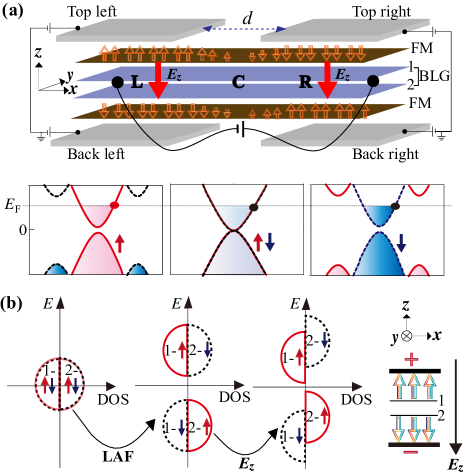
Recent progress made it possible to fabricate 2D structures composed of almost any layers on top of each other LiYang ; ZhongSey ; NovMish . These structures display a higher variety of properties than natural materials, can be tailored to have predefined physical properties, and open a way to design high-performance devices based on unusual interface physics. Motivated by the latest advances on fabrication of four-layer vdW heterosystems (typically graphene/bilayer CrI3/graphene SongCai and WSe2/bilayer graphene (BLG)/WSe2 Island ) and a BLG-based device that allows for local bias control LiWang , we propose an artificial four-layer LAF device [Fig. 1(a)] with two gated terminals linked by the central scattering region to realize a fully electrically controlled spin valve. Its operation mechanism is similar to that of existing giant MR devices Grunberg ; YeZhu ; ModMog ; LuoM ; LinYang ; CarSor ; SongCai ; HanKaw0 , with the difference that it does not require magnetic field: By altering the mutual bias orientation in the two terminals, from P to AP, the MR of in-plane transport varies significantly. Due to the magneto-electric coupling [Fig. 1(b)], the spin valve effect is transferred to the nonmagnetic vdW layers. We start with a phenomenological model, and further use the density functional theory (DFT) calculations to demonstrate the concept with a material platformBLG encapsulated by two single layers of CGT.
Our proposed LAF spin valve has three advantages over the usual spin valves Grunberg ; YeZhu ; ModMog ; LuoM ; LinYang ; CarSor ; SongCai ; HanKaw0 : () It is robust against environmental perturbations from magnetic or null-stray fields due to antiferromagnetism BalMan ; JungMar ; GongSJ ; () It requires only small vertical bias to control, is reversible to operate, superior to traditional magnetic control Grunberg ; () It is not sensitive to the presence of domain walls (DWs), thus enabling the device to possess strong anti-jamming of DWs. The two latter points are not trivial, and we demonstrate their validity here.
II Model and Theory
Our model of four vdW layers in Fig. 1(a) contains the nonmagnetic conducting BLG with Bernal stacking McKosh ; Neto in the middle and two FM insulating layers located respectively on the upper and lower sides. As a typical conducting system, BLG has the advantages of highly-adjustable electron mobility McKosh ; ZhaTan and long spin relaxation length HanKaw ; Suichen ; XuZhu , which can be very little affected by vdW proximity Island ; YangTu and suggest an easily-prepared platform to realize low-consumption devices. We assume that the two insulating layers are identical 2D magnets with out-of-plane magnetization (favorable to ultrahigh density data storage WelMos ), and do not contribute to the low-energy electronic bands except for proximity-induced magnetism. An effective low-energy Hamiltonian from an empirical tight-binding model (see Appendix A) reads
| (1) |
where , , () are, respectively, the Pauli matrices for sublattice isospin, layer isospin and real spin. Here, indicate two opposite valleys , of the hexagonal Brillouin zone, is the momentum component, is the Fermi velocity in graphene (, are the bond length and nearest-neighbor hopping, respectively), and , and denote the strengths of the interactions. The first and second terms are, respectively, the massless Dirac term and the interlayer nearest-neighbor coupling (usually sufficient to capture the band features McKosh ; Neto ). The third term indicates the LAF field induced by short-range magnetic proximity from two FM layers TangZhang ; CarSor . The last term represents the vertical bias.
We also consider other possible interactions which might be present but do not qualitatively change the MR effect we concern with. They read KarpCum ; Island ; YangTu , where represents the intralayer inversion-symmetry breaking induced by interface lattice mismatch and KarpCum ; ZhaiJin1 ; ZhaiJin2 is the proximity-induced Rashba interaction. For simplicity, we take the same in both monolayers. Disregarding , the low-energy four bands are solved as
| (2) |
where ( denote spin up and spin down, respectively). In the actual numerical calculations below (Fig. 2), weak is taken into account as well.
As sketched in Fig. 1(a), the system is divided into three regions, including the left (L), right (R) terminals and the central (C) scattering region. We use an effective empirical potential SanPra and , respectively, to simulate the AP and P bias configurations. Here, erf is the error function, and is the center of region C.
Depending on the sample quality, the system can be a pristine LAF crystal when no DW is present in region C (). The simplest DW is collinear, as sketched in Fig. 1(a), and can be simulated by a smooth potential WahAug
| (3) |
Here, the magnetization vanishes at due to the destructive overlap between opposite spins. We can further consider the noncollinear Bloch (, ) and Néel (, ) types of DW due to spin fluctuation WahAug by adding in-plane magnetization terms and to Eq. (1), respectively. The in-plane magnetization of Bloch (Néel) type is parallel (perpendicular) to the DW, and the sign of or indicates the DW chirality. The spin valve functions qualitatively the same with or without DWs, however, the details of scattering potential differ.
Taking the collinear DW in Fig. 1(a) for example, we illustrate a typical band-to-band tunneling to realize the high MR state for the P bias configuration due to spin mismatch between L and R. By tuning the direction of vertical bias, the LAF spin valve can be switched on or off. The giant MR effect is understood from a general picture of phase transition in Fig. 1(b), seen from model (1), that the LAF field drives BLG to be insulating by moving the states with opposite spins in the same layer and the states with the same spin in opposite layers oppositely. The vertical bias induces a full spin polarization by moving the states in the opposite layers oppositely. More crucial for the realization of the entirely electric control of the spin valve effect is that the opposite bias induces the opposite spin polarization. We characterize the MR effect by a resistance ratio LinYang ; Grunberg
| (4) |
where is the resistance for the P (AP) case. The conductance can be calculated by using the nonequilibrium Green’s function method Datta as
| (5) |
with the transmission given by , where is the Green’s function of the system, Tr denotes the trace, represents the broadening of L and R, and is the Fermi-Dirac distribution function.
III RESULTS AND DISCUSSION
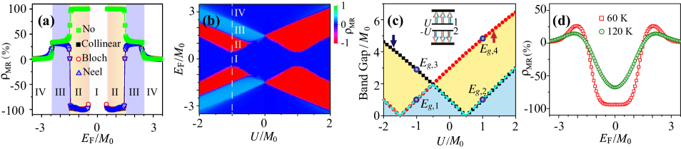
We first solve the model by performing calculations in an armchair-edged sample with the width . Two terminals L and R are assumed to be semi-infinite. A relatively-short scattering region with the length is fixed, and the main electrically-tunable parameters are the bias voltage and the Fermi energy (see details in Appendix B) and Ref. [GavLaz, ]). We keep the same for P and AP configurations and fix the parameters eV and eV from bare GBL Neto and meV, meV and meV.
When meV is fixed ( V/nm ZhaTan ), our results of MR ratio versus in Fig. 2(a) show that nearly-perfect MR effect, i.e. , appears for , independent of whether the DW is present or not. The MR ratio of this spin valve effect changes the sign if a DW appears. This is because the -induced spin polarization near changes sign in terminal R (is unchanged in L). Nontrivially, we find the giant MR effect is not sensitive to whether the DW type is collinear, Bloch or Néel, and meanwhile, the spin valve effect is irrelevant to the magnetic chirality of DW, confirmed by changing the sign of or in calculations. To illustrate the MR effect in more detail, we show the contour plot of MR ratio in the plane for the collinear DW in Fig. 2(b). The result shows that there is a sharp transition between the absence of the MR effect for lower and the nearly-perfect MR effect for higher [see also in Fig. 2(a)]. This parameter regime of no MR, , is attributed to either of the following two factors: One is the absence of transport states induced by band gap in two terminals, and the other is the spin mismatch for both P and AP bias configurations.
To precisely clarify the result in Fig. 2(b), we plot the band gap (green dashed line) for terminal L as a function of in Fig. 2(c). For contrast, we also plot the spin-dependent band gap (circle for spin up, rectangle for spin down) by ignoring in calculations. It is found that the total band gap changes very little if is added due to . In the presence of the DW in Eq. (3), the band gap in terminal R can be directly obtained by interchanging the tabs for opposite spins in Fig. 2(c) due to the opposite magnetic orientation in two terminals. Thus, it is sufficient to get all the information of band gap by analyzing either of two terminals. After sorting four values for terminal L in order from lowest to highest, labeled as (=1 to 4), we find considering the tunnelling mechanism in Fig. 2(b) that MR vanishes (I, ) for , and the nearly-perfect MR (II, ) occurs under the conditions for and for . Likewise, the normal giant MR (III, Grunberg ) holds for , and weak MR (IV, ) happens for .
Without a DW, the dependence of is identical for the two terminals, the condition for MR to vanish in Fig. 2(a) is strictly given by [see the blue region in Fig. 2(c)]. Independent of whether the DW is present or not, the nearly-perfect MR can work for the overlapping band gap region of opposite spins [see the yellow region in Fig. 2(c)] by tuning the magnitude of the bias which can be different for L and R, in addition to the sign of the bias.
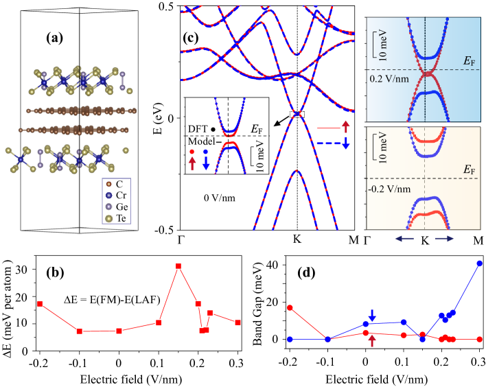
Figure 2(d) further considers the influence of temperature, showing MR at K and 120 K, for the collinear DW at . Unsurprisingly, MR ratio versus becomes smooth due to the presence of the Fermi-Dirac distribution in Eq. (5), in comparison with that in Fig. 2(a). The energy broadening induced by temperature can cover the whole band gap region, and thus enables giant MR effect when lies inside the band gap. Note that the pattern of the curves in Fig. 2(d) remains the same even if the -modified is considered in a specific system. This means, the proposed spin-valve mechanism remains operational up to the Curie temperature of the FM layers.
In particular, the numerical result for the finite-size strip in Fig. 2(c) agrees with the analytical result for the 2D bulk case derived from Eq. (2) for . This reveals a negligible edge effect. Further calculations indicate that the edge effect on band gap can be ignored when exceeds a critical value (5 nm), consistent with the experimental report YinJiang for bare BLG. Additionally, it is argued that the electron mean free path can be estimated by SanPra ( is the Fermi wavelength, nm for ). The spin diffusion length may be estimated by (the Fermi velocity ) in the Dyakonov-Perel mechanism DyaPerel . The ballistic spin transport, on which we deliberately focus here, should always dominate for (see Appendix C, is usually on the scale). The nanoscale and here should be experimentally available YinJiang ; WahAug .
For zigzag-edged systems, the LAF field or vertical bias can induce edge states ZhaiBlanter , which reduce the MR ratio. However, edge disorder or defects can increase the MR ratio by hindering the edge transport. For both the armchair or zigzag-edged systems with , the spin valve effect can still hold in spite of strong quantum confinement, which only leads to some quantitative variations in MR.
IV Proposal for materials realization
We now propose, based on DFT calculations KreFur ; KreFurth ; KreHaf ; PerBur ; TangSan , that BLG encapsulated by CGT monolayers, each of which is a FM semiconductor GongLi ; GoZha , is feasible to realize the antiferromagnetism in our model. There was a previous LAF prediction in CrI3/BLG/CrI3 CarSor , but the formation of mixed low-energy bands from both BLG and CrI3 strongly limits its superiority. For the compounds of graphene and CGT, the influence of spin-orbit couplings on low-energy bands are much smaller than other parameters and can be disregarded, as proved previously ZolGmi ; ZolGmi20 .
In Fig. 3, we show the DFT results for CGT/BLG/CGT with an average equilibrium interlayer spacing between CGT monolayer and its close-contacted graphene monolayer. The unit cell in Fig. 3(a) is constructed with a supercell of 50 carbon atoms per graphene layer and a supercell of 12 chromium atoms per CGT layer. See Appendix D for other computable details. To clarify the magnetism of the ground state, we show the energy difference on average per atom () between the FM and LAF states in Fig. 3(b), which strongly suggests that the system has a LAF ground state robust against small that we focus on. In contrast, bilayer CGT itself is FM GongLi , which becomes LAF here when the layers are spatially separated.
We show the DFT band at in the left panel of Fig. 3(c), where the inset enlarges the local band near and is well fitted by meV, meV, eV, eV in our model and an additional interlayer next-nearest neighboring hopping eV. Here, we have and , different from the assumptions in Fig. 2. As expected, we show the contrasting spin polarization of the bands for V/nm, which is much smaller than 13 V/nm experimentally accessible in vdW systems of BLG ZhaTan and bilayer CrI3 JiangLi . We plot the spin-dependent band gap versus in Fig. 3(d), where spin-up and spin-down band gaps vanish for V/nm and V/nm, respectively. This is beyond our model because CGT has a nonnegligible contribution to as increases.
V Conclusion
Our proposal of antiferromagnetic spin valve based on vdW magnetic proximity effect paves the way for engineering spintronic devices with low energy consumption by making full use of magneto-electric coupling. The appearance of nearly-perfect MR and the robustness of antiferromagneism against required vertical bias have revealed the superiority of our proposed device. Other adjustable quantities, e.g. stacking order, interlayer sliding, rotation angle or layer number, may bring rich opportunities for developing 2D antiferromagnetic spintronics.
ACKNOWLEDGMENTS
This work was supported by the NSFC with Grant Nos. 12074193, 61874057 and 11874059, the QingLan Project of Jiangsu Province (2019), Key Research Program of Frontier Sciences, CAS, Grant No. ZDBS-LY-7021, Beijing National Laboratory for Condensed Matter Physics, Natural Science Foundation of Zhejiang Province (Grant No. LR19A040002). We are grateful to S. Jiang for insightful experimental discussion.
References
- (1) D. J. Monsma, J. C. Lodder, Th. J. A. Popma, and B. Dieny, Perpendicular hot-electron spin-valve effect in a new magnetic-field sensor: the spin-valve transistor, Phys. Rev. Lett. 74, 5260 (1995).
- (2) B. G. Park, J. Wunderlich, X. Martí, V. Holý, Y. Kurosaki, M. Yamada, H. Yamamoto, A. Nishide, J. Hayakawa, H. Takahashi, A. B. Shick, and T. Jungwirth, A spin-valve-like magnetoresistance of an antiferromagnet-based tunnel junction, Nat. Mater. 10, 347 (2011).
- (3) P. A. Grünberg, Nobel lecture: from spin waves to giant magnetoresistance and beyond, Rev. Mod. Phys. 80, 1531 (2008).
- (4) H. Ye, Y. Zhu, D. Bai, J. Zhang, X. Wu, and J. Wang, Spin valve effect in VN/GaN/VN van der Waals heterostructures, Phys. Rev. B 103, 035423 (2021).
- (5) M. Modarresi, A. Mogulkoc, Y. Mogulkoc, and A. N. Rudenko, Lateral spin valve based on the two-dimensional CrN/P/CrN heterostructure, Phys. Rev. Appl. 11, 064015 (2019).
- (6) M. Luo, Antiferromagnetic spin valve based on a heterostructure of two-dimensional hexagonal crystals, Phys. Rev. B 99, 165407 (2019).
- (7) X. Lin, W. Yang, K. L. Wang, and W. Zhao, Two-dimensional spintronics for low-power electronics, Nat. Electron. 2, 274 (2019).
- (8) T. Song, X. Cai, M. W.-Y. Tu, X. Zhang, B. Huang, N. P. Wilson, K. L. Seyler, L. Zhu, T. Taniguchi, K. Watanabe, M. A. McGuire, D. H. Cobden, D. Xiao, W. Yao, and X. Xu, Giant tunneling magnetoresistance in spin-filter van der Waals heterostructures, Science 360, 1214 (2018).
- (9) C. Cardoso, D. Soriano, N. A. García-Martínez, and J. Fernández-Rossier, Van der Waals Spin Valves, Phys. Rev. Lett. 121, 067701 (2018).
- (10) W. Han, R. K. Kawakami, M. Gmitra, and J. Fabian, Graphene spintronics, Nat. Nanotchnol. 9, 794 (2014).
- (11) C. Gong, L. Li, Z. Li, H. Ji, A. Stern, Y. Xia, T. Cao, W. Bao, C. Wang, Y. Wang, Z. Q. Qiu, R. J. Cava, S. G. Louie, J.Xia, and X. Zhang, Discovery of intrinsic ferromagnetism in two-dimensional van der Waals crystals, Nature 546, 265 (2017).
- (12) B. Huang, G. Clark, E. Navarro-Moratalla, D. R. Klein, R. Cheng, K. L. Seyler, D. Zhong, E.Schmidgall, M. A. McGuire, D. H. Cobden, W. Yao, D. Xiao, P. Jarillo-Herrero, and X. Xu, Layer-dependent ferromagnetism in a van der Waals crystal down to the monolayer limit, Nature 546, 270 (2017).
- (13) K. S. Burch, D. Mandrus, and J.-G. Park, Magnetism in two-dimensional van der Waals materials, Nature 563, 47 (2018).
- (14) C. Gong and X. Zhang, Two-dimensional magnetic crystals and emergent heterostructure devices, Science 363, 706 (2019).
- (15) S. Jiang, J. Shan, and K. F. Mak, Electric-field switching of two-dimensional van der Waals magnets, Nat. Mater. 17, 406 (2018).
- (16) S. Jiang, L. Li, Z. Wang, K. F. Mak, and J. Shan, Controlling magnetism in 2D CrI3 by electrostatic doping, Nat. Nanotechnol. 13, 549 (2018).
- (17) Z. Sun, Y. Yi, T. Song, G. Clark, B. Huang, Y. Shan, S. Wu, D. Huang, C. Gao, Z. Chen, M. McGuire, T. Cao, D. Xiao, W.-T. Liu, W. Yao, X. Xu, and S. Wu, Giant nonreciprocal second-harmonic generation from antiferromagnetic bilayer CrI3, Nature 572, 497 (2019).
- (18) V. Baltz, A. Manchon, M. Tsoi, T. Moriyama, T. Ono, and Y. Tserkovnyak, Antiferromagnetic spintronics, Rev. Mod. Phys. 90, 015005 (2018).
- (19) T. Jungwirth, X. Marti, P. Wadley, and J. Wunderlich, Antiferromagnetic spintronics, Nat. Nanotechnol. 11, 231 (2016).
- (20) S.-J. Gong, C. Gong, Y.-Y. Sun, W.-Y. Tong, C.-G. Duan, J.-H. Chu, and X. Zhang, Electrically induced 2D half-metallic antiferromagnets and spin field effect transistors, Proc. Natl. Acad. Sci. 115, 8511 (2018).
- (21) X. Zhai and Y. M. Blanter, Spin-valley polarized quantum anomalous Hall effect and a valley-controlled half-metal in bilayer graphene, Phys. Rev. B 101, 155425 (2020).
- (22) J. Li, X. Yang, Y. Liu, B. Huang, R. Wu, Z. Zhang, B. Zhao, H. Ma, W. Dang, Z. Wei, K. Wang, Z. Lin, X. Yan, M. Sun, B. Li, X. Pan, J. Luo, G. Zhang, Y. Liu, Y. Huang, X. Duan, and X. Duan, General synthesis of two-dimensional van der Waals heterostructure arrays, Nature 579, 368 (2020).
- (23) D. Zhong, K. L. Seyler, X. Linpeng, R. Cheng, N. Sivadas, B. Huang, E. Schmidgall, T. Taniguchi, K. Watanabe, M. A. McGuire, W. Yao, D. Xiao, K.-M. C. Fu, and X. Xu, Van der Waals engineering of ferromagnetic semiconductor heterostructures for spin and valleytronics, Sci. Adv. 3, e1603113 (2017).
- (24) K. S. Novoselov, A. Mishchenko, and A. Carvalho, 2D materials and van der Waals heterostructures, A. H. Castro Neto, Science 353, 461 (2016).
- (25) J. O. Island, X. Cui, C. Lewandowski, J. Y. Khoo, E. M. Spanton, H. Zhou, D. Rhodes, J. C. Hone, T. Taniguchi, K. Watanabe, L. S. Levitov, M. P. Zaletel, and A. F. Young, Spin-orbit-driven band inversion in bilayer graphene by the van der Waals proximity effect, Nature 571, 85 (2019).
- (26) J. Li, K. Wang, K. J. McFaul, Z. Zern, Y. Ren, K. Watanabe, T. Taniguchi, Z. Qiao, and J. Zhu, Gate-controlled topological conducting channels in bilayer graphene, Nat. Nanotechnol. 11, 1060 (2016).
- (27) E. McCann and M. Koshino, The electronic properties of bilayer graphene, Rep. Prog. Phys. 76, 056503 (2013).
- (28) A. H. Castro Neto, F. Guinea, N. M. R. Peres, K. S. Novoselov, and A. K. Geim, The electronic properties of graphene, Rev. Mod. Phys. 81, 109 (2009).
- (29) Y. Zhang, T.-T. Tang, C. Girit, Z. Hao, M. C. Martin, A. Zettl, M. F. Crommie, Y. R. Shen, and F. Wang, Direct observation of a widely tunable bandgap in bilayer graphene, Nature 459, 820 (2009).
- (30) M. Sui, G. Chen, L. Ma, W.-Y. Shan, D. Tian, K. Watanabe, T. Taniguchi, X. Jin, W. Yao, D. Xiao, and Y. Zhang, Gate-tunable topological valley transport in bilayer graphene, Nat. Phys. 11, 1027 (2015).
- (31) W. Han and R. K. Kawakami, Spin Relaxation in Single-Layer and Bilayer Graphene, Phys. Rev. Lett. 107, 047207 (2011).
- (32) J. Xu, T. Zhu, Y. K. Luo, Y.-M. Lu, and R. K. Kawakami, Strong and Tunable Spin-Lifetime Anisotropy in Dual-Gated Bilayer Graphene, Phys. Rev. Lett. 121, 127703 (2018).
- (33) B. Yang, M.-F. Tu, J. Kim, Y. Wu, H. Wang, J. Alicea, R. Wu, M. Bockrath, and J. Shi, Tunable spin-orbit coupling and symmetry-protected edge states in graphene/WS2, 2D Mater. 3, 031012 (2016).
- (34) D. Weller and A. Moser, Thermal effect limits in ultrahigh-density magnetic recording, IEEE Trans. Magn. 35, 4423 (1999).
- (35) C. Tang, Z. Zhang, S. Lai, Q. Tan, and W.-B. Gao, Magnetic proximity effect in graphene/CrBr3 van der Waals heterostructures, Adv. Mater. 32, 1908498 (2020).
- (36) B. Karpiak, A. W. Cummings, K. Zollner, M. Vila, D. Khokhriakov, A. M. Hoque, A. Dankert, P. Svedlindh, J. Fabian, S. Roche, and S. P. Dash, Magnetic proximity in a van der Waals heterostructure of magnetic insulator and graphene, 2D Mater. 7, 015026 (2020).
- (37) X. Zhai and G. Jin, Reversing Berry phase and modulating Andreev reflection by Rashba spin-orbit coupling in graphene mono- and bilayers, Phys. Rev. B 89, 085430 (2014).
- (38) X. Zhai and G. Jin, Proposal for realizing the quantum spin Hall phase in a gapped graphene bilayer, Phys. Rev. B 93, 205427 (2016).
- (39) P. San-Jose, E. Prada, E. McCann, and H. Schomerus, Pseudospin valve in bilayer graphene: towards graphene-based pseudospintronics, Phys. Rev. Lett. 102, 247204 (2009).
- (40) D. A. Wahab, M. Augustin, S. M. Valero, W. Kuang, S. Jenkins, E. Coronado, I. V. Grigorieva, I. J. Vera-marun, E. Navarro-Moratalla, R. F. L. Evans, K. S. Novoselov, and E. J. G. Santos, Quantum Rescaling, Domain Metastability, and Hybrid Domain-Walls in 2D CrI3 Magnets, Adv. Mater. 2004138 (2020).
- (41) S. Datta, Electronic Transport in Mesoscopic Systems (Cambridge University Press, Cambridge, UK, 1995).
- (42) P. Gava, M. Lazzeri, A. M. Saitta, and F. Mauri, Ab initio study of gap opening and screening effects in gated bilayer graphene, Phys. Rev. B 79, 165431 (2009).
- (43) L.-J. Yin, H. Jiang, J.-B. Qiao, and L. He, Direct imaging of topological edge states at a bilayer graphene domain wall, Nat. Commun. 7, 11760 (2016).
- (44) M. I. Dyakonov and V. I. Perel, Spin relaxation of conduction electrons in nancentrosymmetric semiconductors, Sov. Phys. Solid State 13, 3023 (1972).
- (45) G. Kresse and J. Furthmüller, Efficient iterative schemes for ab initio total-energy calculations using a plane-wave basis set, Phys. Rev. B 54, 11169 (1996).
- (46) G. Kresse and J. Furthmüller, Efficiency of ab-initio total energy calculations for metals and semiconductors using a plane-wave basis set, Comput. Mater. Sci. 6, 15 (1996).
- (47) G. Kresse and J. Hafner, Ab initio molecular dynamics for liquid metals, Phys. Rev. B 47, 558 (1993).
- (48) J. P. Perdew, K. Burke, and M. Ernzerhof, Generalized gradient approximation made simple, Phys. Rev. Lett. 77, 3865 (1996).
- (49) W. Tang, E. Sanville, and G. Henkelman, A grid-based Bader analysis algorithm without lattice bias, J. Phys.: Condens. Matter 21, 084204 (2009).
- (50) K. Zollner, M. Gmitra, and J. Fabian, Electrically tunable exchange splitting in bilayer graphene on monolayer Cr2X2Te6 with XGe, Si, and Sn, New J. Phys. 20, 073007(2018).
- (51) K. Zollner, M. Gmitra, and J. Fabian, Swapping exchange and spin-orbit coupling in 2D van der Waals heterostructures, Phys. Rev. Lett. 125, 196402 (2020).