Gate-Assisted Phase Fluctuations in All-Metallic Josephson Junctions
Abstract
The discovery that a gate electrode suppresses the supercurrent in purely metallic systems is missing a complete physical understanding of the mechanisms at play. We here study the origin of this reduction in a Superconductor-Normal metal-Superconductor Josephson junction by performing, on the same device, a detailed investigation of the gate-dependent switching probability together with the local tunnelling spectroscopy of the normal metal. We demonstrate that high energy electrons leaking from the gate trigger the reduction of the critical current which is accompanied by an important broadening of the switching histograms. The switching rates are well described by an activation formula including an additional term accounting for the injection of rare high energy electrons from the gate. The rate of electrons obtained from the fit remarkably coincides with the independently measured leakage current. Concomitantly, a negligible elevation of the local temperature is found by tunnelling spectroscopy which excludes overheating scenarios. This incompatibility is resolved by the fact that phase dynamics and thermalization effects occur at different time-scales.
pacs:
74.45.+c, 74.40.GhI Introduction
Understanding the dynamics of quasiparticle excitations in a superconductor and how they interact with the superconducting condensate is important for understanding dissipation mechanisms responsible for decoherence in superconducting devices Lutchyn2006 ; Zgirski2011 . For example, thermally-induced phase slips of the superconducting order parameter or absorption of electromagnetic radiation locally suppress superconductivity, produces quasiparticles and hence decoherence Golubev2008 ; Martinis2009 ; Vepsalainen2020 ; Cardani2021 . Whereas the injection of low energy quasiparticles (meV) in mesoscopic superconductors has been extensively studied Beckmann2004 ; Cadden2007 ; Kleine2010 ; Quay2013 , little is known about the injection of high energy (eV) quasiparticles Alegria2020 , especially in the limit of few quanta.
Recently, it has been observed that the critical current of a superconducting weak link formed by a mesoscopic nanowire or constriction DeSimoni2018 ; Paolucci2018 ; Paolucci2019 ; DeSimoni2019 ; Paolucci2019bis ; Puglia2020 ; Rocci2020 ; Paolucci2020bis , can be suppressed by applying a voltage bias to a side gate in the vicinity of the weak link. This all metal-based superconducting device, which at first sight seems to operate like a semiconducting field effect transistor, could be used in quantum technologies as a tunable inductance or switch provided dissipation is demonstrated to be low Morpurgo1998 ; Lee2003 ; Wagner2019 . Beyond such practical implications, the understanding of this unexpected effect is attracting a lot of attention. In particular, even though it is still disputed, there is indirect evidence that the leakage current of high energy electrons from the gate plays a major role in reducing the critical currents of mesoscopic constrictions Golokolenov2020 ; Alegria2020 ; Ritter2020 ; Ritter2021 .
The goal of this article is to investigate the transition regime in which a supercurrent reduction is induced by a small ( fA), high energy, quasiparticles leakage rate which already demonstrates a sizeable and puzzling reduction of the supercurrent. In particular, we make use of complementary tools (tunnelling spectroscopy Giaever1960 ; Pothier1997 ; Lesueur2008 and switching probability histograms) to study the gate-induced modulation of the supercurrent in a superconductor-normal metal-superconductor (SNS) Josephson junction. A side gate allows us to attenuate the critical current of the junction in a way similar to previous studies DeSimoni2018 ; Paolucci2018 ; Paolucci2019 ; DeSimoni2019 ; Paolucci2019bis ; Puglia2020 ; Rocci2020 ; Paolucci2020bis ; Ritter2020 ; Golokolenov2020 ; Alegria2020 ; Ritter2021 . The SNS junction contains a tunnel electrode to perform tunnel spectroscopy of the proximitized region. We demonstrate that a current leakage from the gate to the normal metal triggers a supercurrent reduction. This leakage current is composed of rare () and high energy () electrons. It is accompanied by a large broadening of the switching histograms Puglia2020 while, at the same time, a small elevation ( mK for eV) of the local time-averaged electron temperature is found by tunnelling spectroscopy, excluding a simple overheating scenario Alegria2020 . Instead, each high energy electron reaching the junction generates a large temperature spike. The small spike rate combined with the high probability of premature switching to the resistive state due to the high energy involved in the spikes leads to an enhancement of the switching rates for small currents. These independent events are however too rare to significantly elevate the time-averaged electron temperature seen by tunnel spectroscopy. The values of the leakage current obtained from this model match the leakage current measured independently with high resolution confirming the soundness of our model. The proposed scenario is similar to the hotspots created by photons acting on superconducting nanowires or Josephson junction based single photon detectors Engel2013 ; McCaughan2019 ; Walsh2021 ; Marsili2016 ; Kadin1996 ; Goltsman2001 .
The article is organized as follows. After presenting the sample fabrication and the measurement setup in section II, we investigate the static properties of the gating effect in section III where we study critical current reduction, leakage current and perform tunnel spectroscopy. We then analyse the phase dynamics in section IV that we compare to a model of independent high energy quasiparticles reaching the weak link. Discussion of the results, including comparison to other experiments is given in section V.
II Sample fabrication and experimental setup
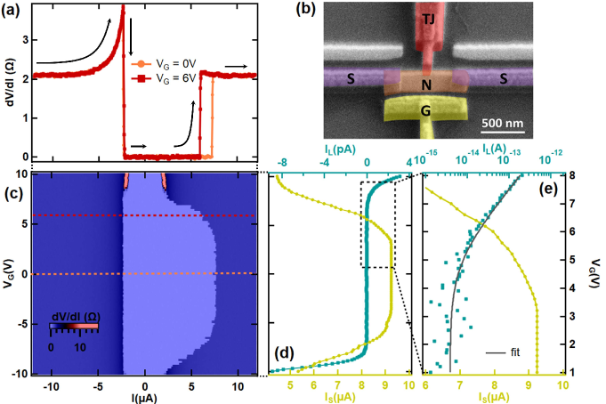
The sample consists of a Superconductor-Normal metal-Superconductor (SNS) Josephson junction tunnel coupled to a superconducting electrode and a side gate (G). All superconducting electrodes are made of Al while the normal metal is Cu. The tunnel junction (TJ) is used to probe the density of states and the local temperature in N Giaever1960 . A typical sample is shown in figure 1(b). The tunnel junction surface is roughly nm nm and the gate is located nm away from the SNS junction. The device is fabricated in a single step e-beam lithography followed by a three angle e-gun evaporation technique. We first deposit a thin nm layer of Al with a positive angle (red in figure 1(b)). This layer is then oxidized in pure oxygen to form a good tunnel barrier with nm of copper evaporated at zero angle (orange) just after oxidation. A third evaporation, at a negative angle, of nm of Al defines the superconducting contacts (violet) as well as the gate electrode (yellow) necessary to tune the supercurrent across the SNS junction. The samples are cooled down in a dilution refrigerator at mK base temperature. Each contacts of the SNS and tunnel junctions are connected through dissipative, highly filtered and closely packed twisted pairs. Of note, the gate electrode is independently connected to a semi-rigid microwave cable to avoid stray leakage currents with the measurement lines (see Supplementary Material for details SM ). The SNS junction normal state resistance is whereas the tunnel junction resistance is M. Therefore the tunnel junction is non invasive for voltages lower than mV where the current reaches roughly 100 pA. From the temperature dependence of the tunneling spectroscopy and the geometry, we estimate the Thouless energy eV and a diffusion time ps.
III Stationary properties
III.1 Gate-dependent supercurrent and leakage current
We first address the gate-induced change of the mean switching current, , by measuring the differential resistance as a function of the current and gate voltage . The results are shown as a colormap in figure 1(c) with line cuts in figure 1(a). As in previous reports, no gate-dependence of is observed below a threshold value which in our case is about V. For V and up to V the switching current is reduced by about 50% while the retrapping current, the current at which the voltage drop snaps back to zero, is unaffected. Above V the hysteresis in the I-V characteristics disappears and . The switching current is suppressed further by increasing . We separately measure, with high accuracy 444Such precision was achieved using an automated differential measurement technique between gate on and off as explained in the supplementary materials SM , the leakage current from the gate , as a function of the gate voltage (figure 1(d) and (e)). These data demonstrate a clear correlation between the critical current reduction and the leakage current.
III.2 Tunnelling spectroscopy
In order to show that the reduction of the switching current is not due to overheating, we first measure its temperature and gate dependence and shown in figure 2(a). We then estimate, in a second time, the increase of the electronic temperature due to the gate voltage by tunnelling spectroscopy. The comparison of the temperature and gate datasets allow us to conclude that overheating is, in the limit of small leakage current, a negligible source of reduction of the critical current.
To access experimentally the electronic temperature of the normal metal region, we perform tunnel spectroscopy by measuring the non-linear conductance of the tunnel contact coupled to the N part of the SNS junction (see figure 1(b)) as a function of gate voltage (figure 2(b)) and temperature (figure 2(c)). In this geometry, the quasiparticles current that flows through the junction is given by:
| (1) |
where is the Al BCS density of states and is the density of states in N as modified by the proximity effect. and are the distribution functions. Assuming that and are the Fermi-Dirac distribution functions at the bath temperature and at , respectively, the tunnel current is a direct probe of the time-averaged electron temperature in the normal metal. According to equation (1), a rounding of the distribution function, due to an increase of shall be visible for a voltage bias of the tunnel junction where eV is the Al superconducting gap and eV is the mini-gap induced in N Lesueur2008 .
We show in figure 2(b) the differential conductance of the tunnel probe as a function of bias voltage for different gate voltages. At the lowest temperature, and only in the extreme case of high gate voltage V, a small modification of the differential conductance is visible corresponding to a slight overheating of N.
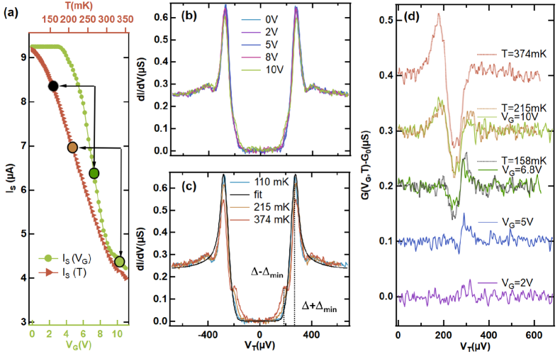
To estimate , we compare these gate-dependent datasets to the ones obtained as a function of the bath temperature reported in figure 2(c). The temperature dependence is well captured by equation (1). In particular, the high temperature curve exhibits a peak in the differential conductance at when the bath temperature becomes comparable with the minigap . This peak comes from thermal quasiparticles in N. Because the deviations from equilibrium are small we show in figure 2(d) the numerical difference where . This difference shows that gating starts to raise the temperature from V. We see experimentally that for V, the increase in is about 50 mK and 100 mK for V as can be seen through the perfect overlaps shown in figure 2(d). At the same time, even though the tunneling data coincide, strong differences are observed in the mean switching current (see dots in figure 2(a)) which is a first hint that the large gate-induced supercurrent reduction observed experimentally cannot be explained by a simple overheating Alegria2020 ; Catto2021 .
We now relate the small raise of temperature to the leakage current. For that we estimate the increase in the average electron temperature in the junction due to a flow of high energy electrons. At V where the leakage current reaches , we get with the energy relaxation time and K the temperature spike generated by a single high energy quasiparticle according to where , is the Sommerfeld constant of N and the diffusion volume ( cm3). The relaxation time in our case is ns, the time for the high energy quasiparticles to escape the same diffusion volume 555This volume includes both the Copper junction but also the small Al contacts until the larger contacts sink the electrons. The small Al leads need to be taken into account because of the high energy of the electrons which are not bound to Copper. This crude estimation of the temperature rise is comparable to the value obtained by tunnelling spectroscopy.
IV Switching dynamics
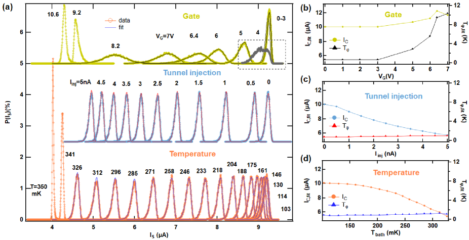
We have seen in the previous section that the effect of the gate on the temperature is negligible while the switching current is strongly reduced. This suggests that the phase of the junction is driven out-of-equilibrium by the gate. In order to confirm this out-of-equilibrium scenario, we investigate the switching dynamics. To address the gate-induced superconducting phase dynamics Stewart1968 ; McCumber1968 , we measure the switching probability histograms for a different set of control parameters (e.g , , …). To do so, we repeatedly (M times) current bias the SNS junction with a sawtooth signal varying from 0 to 10 A and back at the frequency Hz. The junction switches to a resistive state with a certain probability . We show in figure 3 the histograms obtained for different gate voltages, temperatures and low-energy quasiparticle injection currents.
The switching probability can be written as a function of the escape rate as Kurkijarvi1972 ; Fulton1974 :
| (2) |
where is the speed of the current bias ramp. In the thermally activated regime, the escape rate is given by Kramers1940 ; Stewart1968 ; McCumber1968 :
| (3) |
where is the potential barrier defined by the tilted-washboard potential, is the current dependent plasma frequency and is the phase temperature, which can be higher than the time-averaged electron temperature , due to out-of-equilibrium current noise (see Supplementary Materials for more details SM ; Heikkila2002 ; Basset2019 ).
We first verify that the temperature dependence of the histograms is well captured by the thermal rate expression (3). The histograms (orange color in figure 3(a)) slightly broaden and shift to lower current values when the temperature is raised from 100 mK up to roughly 325 mK. Above 330 mK a sharpening of the histograms is observed as the phase dynamics changes from switching to diffusion because of dissipation Krasnov2005 ; Mannik2005 . The transition between these two regimes occurs at a temperature corresponding to the mini-gap, as expected, since the number of thermal quasiparticles in N is strongly increased for . In the restricted range of low temperatures, the histograms are fitted using the thermal rate given in equation (3). The critical current and the effective phase temperature extracted from the fits are shown in figure 3(d). diminishes from 10 A down to 5 A while the phase temperature increases from 800 mK up to 1200 mK. The same analysis can be done for quasiparticles injection from the tunnel junction where a thermal fit reproduces the data using the parameters shown in figure 3(c). This comparison confirms that injecting low energy quasiparticles ( meV) is equivalent to raising the average temperature, 666Note that this tunnel current injection corresponds to a voltage ( mV) across the tunnel junction higher than that used for the spectroscopic experiment ( mV) presented above and for which the injected current was too small to perturb the switching mechanism..
Comparing the gate dependence to the temperature dependence (figure 3(a)), the same reduction of the mean switching current by gate voltage leads to much broader histograms Puglia2020 ; Ritter2021 . We tentatively fit these histograms using eq.(3). The quality of the fits is reasonable for most gate voltages but fail to explain histograms close to V (see the boxed area at the top of figure 3(a)) where the supercurrent starts to diminish and the histograms are clearly non-thermal. Away from this transient regime, the fitting parameters are shown in figure 3(b). The fitted phase temperature rises to 10 K for the largest gate voltage studied here, this is at least 10 times larger than the equilibrium phase temperature and much larger than the electronic temperature observed in tunnelling spectroscopy reported in section III.2. Note also that the increase in obtained from the fits is not physical but effectively compensates the huge increase in the width of histograms. Finally, we also used the tunnel probe to study the combined action of injecting low energy quasiparticles, equivalent to raising the effective temperature, and high energy electrons leaking from the gate (see Supplementary Material SM ). In conclusion, the fitting parameters using eq.(3) are not physical and confirm that a more sophisticated model than overheating is necessary, especially for the transition regime ( V) where the histograms cannot be fitted.
To do so, we assume, similarly to single photon detectors Walsh2021 , that electrons coming from the gate generates temperature spikes of amplitude equivalent to hot spots 777The effect of the high energy electrons leaking from the gate is modelled by a Poissonian time distribution of the temperature spikes. This reflects the statistics of an independent flow of high energy electrons for small leakage currents. These spikes induce phase fluctuations and do not necessarily switch the junction to the dissipative state if damping is sufficiently high as corroborated by numerical solution of the RCSJ model (see Supplementary Material SM ).. The escape rate associated with the gate leakage current is then given by multiplied by the escape probability that we choose here to be a thermal escape probability with a temperature . With these assumptions, the total escape rate is:
| (4) |
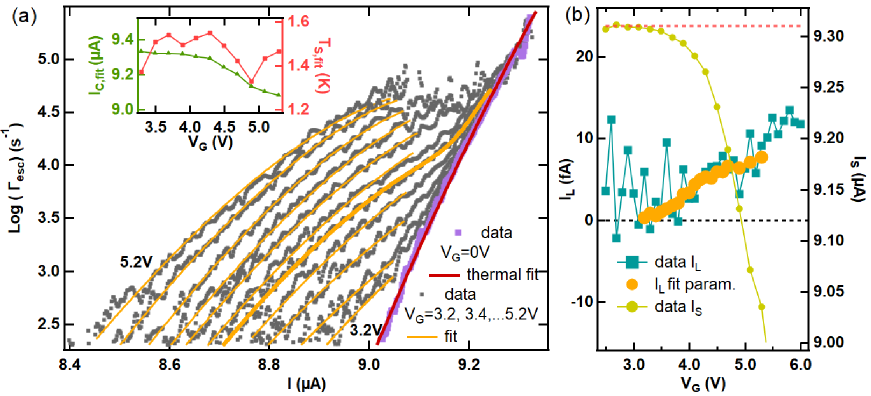
For a more direct comparison of the data to eq. (4) we extract the escape rates as a function of from the switching histograms inverting eq. (2) 888We verified first that the escape rate is independent on the ramp frequency (while the histograms do, see the Supplementary material SM for details). The escape rates for different gate voltages are shown in Figure 4 in the regime of weak leakage current 999weak leakage currents corresponds to a negligible increase of the time-averaged electron temperature and very likely to a leakage current of uncorrelated electrons as supposed in equation (4), V. The log scale graph 4(a) demonstrates that firstly, the logarithm of the escape rates are nearly linear in current bias (thus exponential rates), secondly, they grow as the gate voltage/leakage current is raised and thirdly, each curves seems shifted to one another. Using the second term of eq.(4), we fit our data with the leakage current , the spike temperature and as fitting parameters. For V (purple dots) the data are well fitted (red line) using only the first term of eq.(4) and the same parameters ( and ) as for the histograms shown in figure 3. Increasing requires the second term of eq. (4) which even becomes dominant. Using both terms in the fitting procedure perfectly reproduces our experimental data (gray dots and orange lines in figure 4). Importantly, whereas and allow to tackle the full shape of the curve, fixes the shift between the curves. The values of obtained from the fits as a function of are reported as orange markers in figure 4(b). They follow well the leakage current measured with a room temperature current amplifier also shown in Figure 4(b). The parameters and are shown in the inset of figure 4(a). Interestingly, we find a quasi gate-independent which is very close from the inferred K estimated at V using the formula proposed at the end of section III.
V Discussions and comparison to other experiments
Researchers from University of Lancaster Golokolenov2020 (see also Catto2021 ) recently measured the real and imaginary part of the microwave impedance of a gated Josephson weak link. They show that the field-effect induces large 1/f noise of the microwave impedance. This is coherent with gate-induced non-thermal phase fluctuations. Additionally, the spatially resolved suppression of the critical current reported in reference Ritter2020 has been attributed to current leakage from the gate. An even more recent work Ritter2021 emphasizes that the high energy phonons excited by a remote source of high energy electrons alter the supercurrent the same way as a local gate does. This implies that this is the energy brought by the electron that matters and is qualitatively consistent with the temperature spike scenario proposed here. It is however not clear yet, which is the exact microscopic mechanism at the origin of the leakage current. Some recent studies report that it follows the Fowler-Nordheim model of electron field emission from a metal electrode Golokolenov2020 ; Alegria2020 . In our case (see supplementary material SM ) but also in Ritter2021 this does not seem to be the case and it is more likely that the electrons flow either through the substrate or via surface states.
All these experiments point to out-of-equilibrium effects to explain the gate-induced reduction of the average critical current. We have here emphasized that high energy quasiparticles produce large phase fluctuations visible in the broadening of the switching histograms. Finally, if the leak rate is higher than the relaxation rate the temperature spikes overlap and a global overheating takes place Alegria2020 . From our experiment it is not possible to discriminate between charge and energy fluctuations induced by the leakage current, or in other words between the voltage and temperature pulses associated with absorption of hot electrons from the gate. However it is likely that energy imbalance is more relevant than charge imbalance simply because the estimated temperature spike in the normal wire resulting from a 5 eV electron is which sets an energy scale much larger than the chemical potential change that we estimate to eV.
VI Conclusion
To conclude, we have performed an experiment to probe the field-effect in a metallic Josephson junction by two complementary means, tunnelling spectroscopy and switching histograms. Our experiment reveals that the gate-controllable switching current is triggered by high energy electrons leaking from the gate to the Josephson junction. Their effect is not equivalent to overheating but instead to locally-induced large energy fluctuations which translate in large phase fluctuations visible in the switching histograms. From the escape rates given by the histograms we could extract the leakage current which is in agreement with direct measurements. These findings clarify the local dynamics of high energy quasiparticles and sheds light on the complex mechanisms at play in gated metallic Josephson junctions.
Acknowledgements
We thank F. Giazotto, B. Reulet for fruitful discussions and F. Paolucci, F. Giazotto for providing some SNS samples at the beginning of this work. This research has been funded by a ANR JCJC (SPINOES) grant from the Agence Nationale de la Recherche.
References
- (1) R. Lutchyn, L. Glazman, and A. Larkin, Kinetics of the superconducting charge qubit in the presence of a quasi-particle, Phys. Rev. B 74, 064515 (2006).
- (2) M. Zgirski, L. Bretheau, Q. Le Masne, H. Pothier, D. Esteve, and C. Urbina, Evidence for Long-Lived Quasiparticles Trapped in Superconducting Point Contacts, Phys. Rev. Lett. 106, 257003 (2011).
- (3) D. S. Golubev and A. D. Zaikin, Thermally activated phase slips in superconducting nanowires, Phys. Rev. B 78, 144502 (2008).
- (4) J. M. Martinis, M. Ansmann, and J. Aumentado, Energy decay in superconducting josephson-junction qubits from nonequilibrium quasiparticle excitations, Phys. Rev. Lett. 103, 097002 (2009).
- (5) A.P. Vepsalainen, A.H. Karamlou, J.L. Orrell et al., Impact of ionizing radiation on superconducting qubit coherence, Nature 584, 551–556 (2020).
- (6) L. Cardani, F. Valenti, N. Casali, G. Catelani, T. Charpentier, M. Clemenza, I. Colantoni, A. Cruciani, G. D’Imperio, L. Gironi, L. Grünhaupt, D. Gusenkova, F. Henriques, M. Lagoin, M. Martinez, G. Pettinari, C. Rusconi, O. Sander, C. Tomei, A. V. Ustinov, M. Weber, W. Wernsdorfer, M. Vignati, S. Pirro, and I. M. Pop, Reducing the impact of radioactivity on quantum circuits in a deep-underground facility, Nature Communications 12, 2733 (2021).
- (7) D. Beckmann, H. B. Weber, and H. V. Löhneysen, Evidence for Crossed Andreev Reflection in Superconductor-Ferromagnet Hybrid Structures, Phys. Rev. Lett. 93, 197003 (2004).
- (8) P. Cadden-Zimansky, Z. Jiang, and V. Chandrasekhar, Charge imbalance, crossed Andreev reflection and elastic co-tunnelling in ferromagnet/superconductor/normal-metal structures, New J. Phys. 9, 116 (2007).
- (9) A Kleine, A Baumgartner, J Trbovic, D S Golubev, A D Zaikin and C Schönenberger, Magnetic field and contact resistance dependence of non-local charge imbalance, Nanotechnology 21 274002 (2010).
- (10) C. H. L. Quay, D. Chevallier, C. Bena and M. Aprili, Spin imbalance and spin-charge separation in a mesoscopic superconductor, Nature Physics 9, 84–88 (2013).
- (11) L.D. Alegria, C.G.L. Bottcher, A.K. Saydjari et al., High-energy quasiparticle injection into mesoscopic superconductors, Nat. Nanotechnol. 16, 404–408 (2021).
- (12) G. De Simoni, F. Paolucci, P. Solinas, E. Strambini, and F. Giazotto, Metallic supercurrent field-effect transistor, Nature Nanotechnol. 13, 802 (2018).
- (13) F. Paolucci, G. De Simoni, E. Strambini, P. Solinas, and F. Giazotto, Ultra-Efficient Superconducting Dayem Bridge Field-Effect Transistor, Nano Lett. 18, 4195 (2018).
- (14) G. De Simoni, F. Paolucci, C. Puglia, and F. Giazotto, Josephson Field-Effect Transistors Based on All-Metallic Al/Cu/Al Proximity Nanojunctions, ACS Nano 13, 7871 (2019).
- (15) F. Paolucci, G. De Simoni, P. Solinas, E. Strambini, N. Ligato, P. Virtanen, A. Braggio, and F. Giazotto, Magnetotransport Experiments on Fully Metallic Superconducting Dayem-Bridge Field-Effect Transistors, Phys. Rev. Appl. 11, 024061 (2019).
- (16) F. Paolucci, F. Vischi, G. De Simoni, C. Guarcello, P. Solinas, and F. Giazotto, Field-Effect Controllable Metallic Josephson Interferometer, Nano Lett. 19, 9, 6263-6269 (2019).
- (17) C. Puglia, G. De Simoni, and F. Giazotto, Electrostatic Control of Phase Slips in Ti Josephson Nanotransistors, Phys. Rev. Applied 13, 054026 (2020).
- (18) M. Rocci,G. De Simoni, C. Puglia, D. Degli Esposti, E. Strambini, V. Zannier, L. Sorba, and F. Giazotto, Gate-Controlled Suspended Titanium Nanobridge Supercurrent Transistor, ACS Nano, 14, 12621-12628 (2020).
- (19) F. Paolucci, G. De Simoni, P. Solinas, E. Strambini, C. Puglia, N. Ligato, and F. Giazotto, Field-effect control of metallic superconducting systems, AVS Quantum Sci. 1, 016501 (2019).
- (20) A. F. Morpurgo, T. M. Klapwijk, and B. J. van Wees, Hot electron tunable supercurrent Appl. Phys. Lett. 72, 966 (1998).
- (21) S.B. Lee, G.D. Hutchinson, D. A. Williams, D. G. Hasko, and H. Ahmed, Superconducting nanotransistor based digital logic gates Nanotechnology 14, 2, 188 (2003).
- (22) A. Wagner, L. Ranzani, G. Ribeill, and T. A. Ohki, Demonstration of a superconducting nanowire microwave switch, Appl. Phys. Lett. 115, 172602 (2019).
- (23) I. Golokolenov, A. Guthrie, S. Kafanov, Yu. A. Pashkin, and V. Tsepelin, On the origin of the controversial electrostatic field effect in superconductors. Nat. Comm. 12, 2747 (2021).
- (24) M.F. Ritter,A. Fuhrer, D.Z. Haxell et al., A superconducting switch actuated by injection of high-energy electrons. Nat. Commun 12, 1266 (2021).
- (25) M. F. Ritter, N. Crescini, D. Z. Haxell, M. Hinderling, H. Riel, C. Bruder, A. Fuhrer, F. Nichele, On the Role of Out-of-Equilibrium Phonons in Gated Superconducting Switches, arXiv:2106.01816 (2021).
- (26) H. le Sueur, P. Joyez, H. Pothier, C. Urbina, and D. Estève, Phase Controlled Superconducting Proximity Effect Probed by Tunneling Spectroscopy, Phys. Rev. Lett. 100, 197002 (2008).
- (27) I. Giaever, Energy Gap in Superconductors Measured by Electron Tunneling, Phys. Rev. Lett. 5, 147 (1960).
- (28) H. Pothier, S. Guéron, Norman O. Birge, D. Esteve, and M. H. Devoret, Energy Distribution Function of Quasiparticles in Mesoscopic Wires, Phys. Rev. Lett. 79, 3490 (1997).
- (29) F. Marsili, M. J. Stevens, A. Kozorezov, V. B. Verma, Colin Lambert, J. A. Stern, R. D. Horansky, S. Dyer, S. Duff, D. P. Pappas, A. E. Lita, M. D. Shaw, R. P. Mirin, and S. W. Nam, Hotspot relaxation dynamics in a current-carrying superconductor, Phys. Rev. B 93, 094518 (2016).
- (30) A. M. Kadin and M. W. Johnson, Nonequilibrium photon-induced hotspot: A new mechanism for photodetection in ultrathin metallic films, Appl. Phys. Lett. 69, 3938 (1996).
- (31) G. N. Goltsman, O. Okunev, G. Chulkova, A. Lipatov,A. Semenov, K. Smirnov, B. Voronov, A. Dzardanov,C. Williams, and R. Sobolewski, Picosecond superconducting single-photon optical detector, Appl. Phys. Lett. 79,705 (2001).
- (32) A. Engel and A. Schilling, Numerical analysis of detection-mechanism models of superconducting nanowire single-photon detector, J. Appl. Phys. 114, 214501 (2013).
- (33) A. N. McCaughan, V. B. Verma, S. M. Buckley, J. P.Allmaras, A. G. Kozorezov, A. N. Tait, S. W. Nam, and J. M. Shainline, A superconducting thermal switch with ultrahigh impedance for interfacing superconductors to semiconductors, Nat. Electronics 2, 451 (2019).
- (34) E. D. Walsh, W. Jung, G.-H. Lee, D.K. Efetov, B.-I. Wu, K.-F. Huang, T.A. Ohki, T. Taniguchi, K. Watanabe, P. Kim, D. Englund, and K. C. Fong, Josephson junction infrared single-photon detector, Science 372, 6540, pp. 409-412 (2021).
- (35) See Supplementary Material at XXX for additional data and discussions regarding the experimental setup, numerical simulations, switching histograms and the combined action of low and high energy electrons injection.
- (36) W.C. Stewart, Current-voltage characteristics of Josephson junctions, Appl. Phys. Lett. 12, 277 (1968).
- (37) D. E. McCumber, Effect of ac Impedance on dc Voltage-Current Characteristics of Superconductor Weak-Link Junctions, J. Appl.Phys. 39, 3113 (1968).
- (38) J. Kurkijärvi, Intrinsic Fluctuations in a Superconducting Ring Closed with a Josephson Junction, Phys. Rev. B 6, 832 (1972).
- (39) T. A. Fulton and L. N. Dunkleberger, Lifetime of the zero-voltage state in Josephson tunnel junctions, Phys. Rev. B 9, 4760 (1974).
- (40) H.A. Kramers, Brownian motion in a field of force and the diffusion model of chemical reactions, Physica 7, 284 (1940).
- (41) T. T. Heikkilä, J. Särkkä, and F.K. Wilhelm, Supercurrent-carrying density of states in diffusive mesoscopic Josephson weak links, Phys. Rev. B. 66, 184513 (2002).
- (42) J. Basset, M. Kuzmanović, P. Virtanen, T. T. Heikkilä, J. Estève, J. Gabelli, C. Strunk, and M. Aprili, Nonadiabatic dynamics in strongly driven diffusive Josephson junctions, Phys. Rev. Research 1, 032009 (R) (2019).
- (43) V. M. Krasnov, T. Bauch, S. Intiso, E. Hürfeld, T. Akazaki, H. Takayanagi, and P. Delsing, Collapse of Thermal Activation in Moderately Damped Josephson Junctions, Phys. Rev. Lett. 95, 157002 (2005).
- (44) J. Mannik, S. Li, W. Qiu, W. Chen, V. Patel, S. Han, and J. E. Lukens, Crossover from Kramers to phase-diffusion switching in moderately damped Josephson junctions, Phys. Rev. B 71, 220509 (R)(2005).
- (45) Giacomo Catto, Wei Liu, Suman Kundu, Valtteri Lahtinen, and Mikko Möttönen, Microwave response of a metallic superconductor subject to a high-voltage gate electrode, arXiv:2105.08322 (2021).
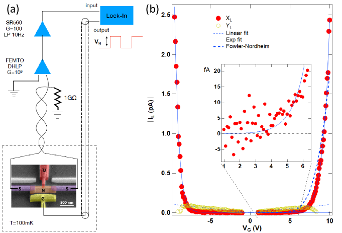
Appendix A Measurement of the gate leakage current
The sample is electrically connected to room temperature connectors using twisted resistive wire pairs (the resistance of each wire is about 100 Ohms). To avoid cross-talk and leakage currents, the gate electrode is independently connected using a semi-rigid coaxial cable which is physically separated from the twisted pairs rope. The leakage current , is measured using the circuit presented in figure A.1(a). To increase the sensitivity, the gate is biased with a TTL signal of amplitude and frequency equals to 50mHz. is then measured using a lock-in amplifier after amplification and low pass filtering (gain = A/V). We verified that a DC measurement of gives the same result with only a worse signal to noise ratio. The absolute values of the in-phase , and out-of phase , components of as a function of are presented in figure A.1(b) for positive and negative values of . Note that the values for negative are actually negative. We also verified that a sweep from zero to 10 V in gate voltage gives the same that a sweep back to zero from 10V. is linear with at low bias as expected for a pure capacitive coupling. The stray capacitance extracted from the fit is C fF. instead is exponential with and corresponds to the dissipative part of the current. The inset of figure A.1(b) shows a zoom of in the range V. These are the data also presented in figure 4 of the main text.
The microscopic mechanism at the origin of the leakage current remains to be elucidated. Cold emission which has been proposed in SAlegria2020 ; SGolokolenov2020 seems unlikely in our case. Indeed, using the Fowler-Nordheim formula SFowler1928 :
| (5) |
where , e, is the work function of N (here Cu), is the electric field, i.e. () poorly fit the experimental data (see figure A.1(b)). More importantly the best fitting parameters give a work function for the gate electrode which is more than one order of magnitude smaller than expected. Using the correct work function, the expected leakage current would be negligible. A better fit of the data is provided using the function
| (6) |
with the coefficients A ( A) , (-1.96 ) and V (-3.25 V) for positive (negative) , respectively. is reminiscent of the I-V characteristics of a diode. This supports that the leakage current flows through the Si/SiO2 substrate and is similar to the leakage current between the gate and the source-drain channels in a Metal Oxide Semiconductor Field Effect Transistor SRalls1984 .
Finally we would like to point out that samples where the distance between the gate and the weak link was about 200 nm did not show any effect on the switching current up to a gate voltage of 120 V.
Appendix B Numerical solution of the RCSJ model with gaussian (thermal) noise and poissonian (shot) noise
We describe the phase dynamics within the RCSJ model SStewart1968 ; SMcCumber1968 in which the Josephson junction is considered as a parallel circuit of three separated components: a resistance that accounts for the dissipative current carried in the weak link by the quasiparticles, a capacitance , and a non-linear inductance due to the finite Josephson current. Following the Kirchhoff’s law, the bias current is divided through these three independent elements. Current conservation translates in an equation for the phase dynamics. Fluctuations are typically accounted by adding a Langevin term that corresponds physically to the thermal noise associated to dissipation in the junction, i.e. the thermal noise of which is a Gaussian noise. The effect of rare high energy electrons leaking from the gate can be included as a Poissonian noise of Dirac current peaks whose amplitude is larger than . This is equivalent to temperature spikes larger than , caused by the absorption of high energy electrons. We here implicitly makes the assumption that energy relaxation is much faster than the average time between two successive events. The stochastic equation governing the phase dynamics can be written as:
| (7) |
where the leakage current is included in the last term . We have introduced the dimensionless bias , the Gaussian Langevin term , the damping parameter and the plasma frequency .
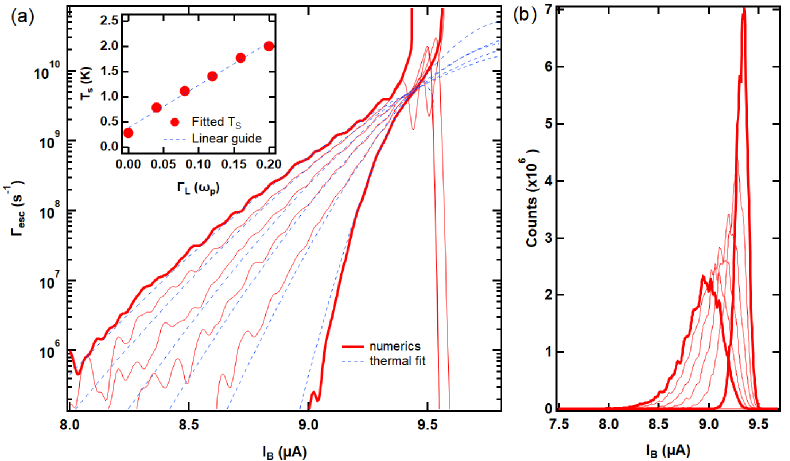
We numerically solve eq.(7) using a Runge-Kutta algorithm SRunge1895 ; SKutta1901 . To construct switching histograms we use a linear ramp for the current bias and repeat the ramp times to get a reasonable statistic. The main technical problem to perform such a numerical investigation is that the plasma frequency is about 8 orders of magnitude larger than the ramp frequency that we used experimentally. To overcome this difficulty, we increase the ramp frequency to and start the ramp sufficiently close from the switching current, to optimize the calculation at currents where the switching probability is sufficiently large. While this procedure is not appropriate to fit the measured histograms, it can however gives some specific insights on the evolution of the histograms and escape rates with increasing leakage current.
We first verified that without Poissonian noise, the Gaussian noise reproduces the thermal histograms, then we added the Poissonian noise. The escape rates and switching histograms obtained numerically are presented in figure B.2(a) and B.2(b) respectively for and increasing the leakage current given in units of the plasma frequency multiplied by the electron charge. We remark that when the frequency of the electrons leaking from the gate is sufficiently high, the associated leakage current, whose statistics is Poissonian, leads to a thermal escape rate in which the phase temperature is much higher than the electron temperature in the Josephson junction. This is particularly clear in the inset of figure B.2(a) where the phase temperature obtained from thermal fits of escape rates is reported as function of leakage rate. Note however that there is a major difference compared to purely thermally-induced switching for which a stronger reduction of the mean value of the switching current is expected. Here instead is only weakly suppressed. This explains the experimental results where the mean value and the variance of the histograms measured as function of the gate voltage and reported in the figure 3 of the main text, are actually uncorrelated. Note also that because of the huge difference in the ramp frequency with respect to the plasma frequency the simulations have been carried out for values of the order of for which indeed we recover experimentally a thermal shape of the histograms. Smaller leakage currents are difficult to simulate and the analytical approach described in the main text turns out to be more appropriate.
Appendix C Switching measurements
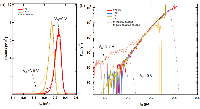
We report in figure C.3(a) the switching histograms measured at two different current bias ramp frequencies, = 17 and 277 Hz for V (thick line) and (thin line) together with fits using the thermal formula (3) in the main text SKurkijarvi1972 ; SFulton1974 for which the critical current and the phase temperature are fitting parameters. From the V fit we get A and mK. figure C.3(b) shows the corresponding escape rates obtained from the histograms SFulton1974 . As expected, while the histograms depend on the speed of the ramp and shift to higher bias current for faster ramps, the rates do not. The reason is that for higher ramp frequencies one explores shorter escape rates as the integrated switching probability is lower for the same bias current, . Note that even in presence of a leakage current induced by a gate voltage, while the histograms are clearly dependent the escape rates are not. To fit the escape rates we use :
| (8) |
where is the potential barrier defined by the tilted-washboard potential. In the case of long diffusive SNS junctions and low temperature the usual cos term has to be replaced by due to the contribution of higher harmonics to the current-phase relation SHeikkila2002 . In the limit , the potential barrier can be approximated by and the plasma frequency, which defines also the attempt frequency to escape, becomes with . The dashed black line in figure C.3(b) is a fit of the data at =0V for which =0 fA while the fitting parameters are the same as for the histograms i.e. and A. The dash-dotted line instead is a fit of the =3.8V rates taking into account the second term in eq.(8) as dominant. The corresponding fitting parameters are fA and . These results have been discussed and analysed in the main text.
Appendix D Combined effect of quasiparticles injection from the tunnel junction and gate
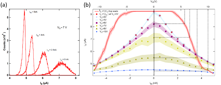
To confirm that the reduction of the switching current, , and the broadening of the switching histograms result from the phase dynamics we intentionally increase the damping by injecting low energy quasiparticles using the tunnel junction. While doing so, we make sure that the injection current is always lower than 5 nA and hence more than three orders of magnitude less than . As such, it acts as a source of out-of-equilibrium quasiparticles while adding a negligible extra current bias to the weak link. We show in figure D.4(a) the switching histograms obtained for =7.0V and different injection currents. From these curves, it is obvious that both the mean value and the variance of the distribution are reduced by increasing the amount of injected quasiparticles. A more complete picture is summarized in figure D.4(b), where we present and the width of the histograms as a function of the injection current , for different values of . As explained in the main text, the injection of low energy quasiparticles in N is equivalent to raising the electron average temperature. Such elevation has two important effects: it decreases the critical current and the resistance within the RCSJ model. A lower is equivalent to increasing the damping and hence the dissipation as described above. Thus, while the reduction of is a direct consequence of the decrease of , the narrowing of the switching histograms is due to the enhanced damping. The shrink of the distribution due to damping finds its origin in the reduction of the attempt frequency in the thermal component of the escape rate. A numerical solution of eq.(7) can also illustrate this result. It is also worth noting that in the case of very high damping the switching distribution becomes a delta function. In the specific case of the leakage current-assisted escape, i.e. the second term of equation (8), the damping does not change the rate of electrons leaking from the gate but reduces the temperature spike, , due to absorption of high energy electrons from the gate and hence reduce the energy fluctuations in N.
References
- (1) I. Golokolenov, A. Guthrie, S. Kafanov, Yu. A. Pashkin, and V. Tsepelin, On the origin of the controversial electrostatic field effect in superconductors. Nat. Comm. 12, 2747 (2021).
- (2) L.D. Alegria, C.G.L. Bottcher, A.K. Saydjari et al., High-energy quasiparticle injection into mesoscopic superconductors, Nat. Nanotechnol. 16, 404–408 (2021).
- (3) R. H. Fowler and L. Nordheim, Electron emission in intense electric fields, P. R. Soc. Lond. A-Conta. 119, 173 (1928).
- (4) K. S. Ralls, W. J. Skocpol, L. D. Jackel, R. E. Howard, L. A. Fetter, R. W. Epworth, and D. M. Tennant, Discrete Resistance Switching in Submicrometer Silicon Inversion Layers: Individual Interface Traps and Low-Frequency (1/f) Noise, Phys. Rev. Lett. 52, 228 (1984).
- (5) W.C.Stewart, Current-voltage characteristics of Josephson junctions, Appl. Phys. Lett. 12, 277 (1968).
- (6) D. E. McCumber, Effect of ac Impedance on dc Voltage-Current Characteristics of Superconductor Weak-Link Junctions, J. Appl.Phys. 39, 3113 (1968).
- (7) C.D.T. Runge, Über die numerische Auflösung von Differentialgleichungen, Mathematische Annalen, Springer 46 (2): 167–178 (1895).
- (8) M. Kutta, Beitrag zur näherungsweisen Integration totaler Differentialgleichungen, Zeitschrift für Mathematik und Physik 46: 435–453 (1901).
- (9) J. Kurkijärvi, Intrinsic Fluctuations in a Superconducting Ring Closed with a Josephson Junction, Phys. Rev. B 6, 832 (1972).
- (10) T. A. Fulton and L. N. Dunkleberger, Lifetime of the zero-voltage state in Josephson tunnel junctions, Phys. Rev. B 9, 4760 (1974).
- (11) T. T. Heikkilä, J. Särkkä, and F.K. Wilhelm, Supercurrent-carrying density of states in diffusive mesoscopic Josephson weak links, Phys. Rev. B. 66, 184513 (2002).