Electronic Self-passivation of Single Vacancy in Black Phosphorus via a Controlled Ionization
Abstract
We report that mono-elemental black phosphorus presents a new electronic self-passivation scheme of single vacancy (SV). By means of low-temperature scanning tunneling microscopy and bond-resolved non-contact atomic force microscopy, we demonstrate that the local reconstruction and ionization of SV into negatively charged leads to the passivation of dangling bonds and thus the quenching of in-gap states, which can be achieved by mild thermal annealing or STM tip manipulation. SV exhibits a strong and symmetric Friedel oscillation (FO) pattern, while shows an asymmetric FO pattern with local perturbation amplitude reduced by one order of magnitude and a faster decay rate. The enhanced passivation by forming can be attributed to its weak dipole-like perturbation, consistent with density-functional theory and numerical calculations. Therefore, self-passivated is electronically benign and acts as a much weaker scattering center, which may hold the key to further enhance the charge mobility of BP and its analogs.
High-mobility two-dimensional semiconductors (2DSCs) are essential for the development of ultra-thin high-speed and energy-efficient electronics and optoelectronics [1, 2, 3, 4, 5]. The intrinsic mobility of defect-free 2DSCs is normally set by the effective mass of carriers and phonon scattering processes [6, 7]. However, materials synthesis and device fabrication processes of 2DSCs, including metal chalcogenides and black phosphorus (BP), inevitably introduce surface vacancies with dangling bonds (DBs) due to the volatile nature of chalcogen and phosphorus (P) atoms [8, 9, 10, 11]. Such atomic defects often act as undesirable sinks for charge carriers and nonradiative recombination centers of photoexcited electron-hole pairs [12, 13, 14], which becomes one of the major device performance limiting factors. Therefore, effective passivation of vacancies in high-mobility 2DSCs is vital to maintaining their high-performance device characteristics.
The ideal surface passivation method should deactivate only the defect states of 2DSCs without a permanent crystal lattice change and degradation of their electronic performance. Inspired by the conventional passivation technologies used in the semiconductor industry, various strategies, including chemical functionalization [7, 15]and surface coating [16, 17], have been exploited for the passivation of surface vacancies in 2DSCs to remove the associated detrimental in-gap electronic states. However, most passivation schemes developed to date mainly improve the photoluminescence quantum yield without significant enhancement in charge transport properties [18, 15], and even degrade the electronic performance by altering the van der Waals structure [19, 16].
Here, we demonstrate that mono-elemental BP, a prototypical high-mobility 2DSC with a unique puckered square lattice [1, 20, 21, 22, 23, 24], is able to effectively passivate isolated vacancies by a self-driven lattice reconstruction process to form negatively charged sites. Such an self-passivation mechanism of vacancies and the associated in-gap electronic states relies on the formation of homoelemental hypervalent bonding, which is not reported in heteroelemental 2DSCs (e.g., metal chalcogenides).
As illustrated in Fig. 1a, removal one P atom from the buckled lattice in BP creates an SV and leaves DBs at three adjacent P sites . Neutral SVs in BP are predicted to possess in-gap electronic states, which play an essential role in modulating electronic and optical properties of BP and thus affecting their device characteristics [25, 26, 27, 11, 28, 29]. Despite advances in BP research, the atomic-scale structural and electronic properties of SVs and their impact on charge dynamics in BP remain elusive. In addition, the microscopic knowledge of defect passivation mechanism for eliminating DBs in SVs of BP is still missing.
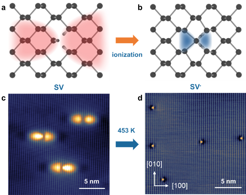
To this end, we have exploited low-temperature scanning tunneling microscopy (STM) and bond-resolved non-contact atomic force microscopy (nc-AFM) to probe the electronic self-passivation of intrinsic SV in BP. The versatile bond configuration of P atoms and mono-elemental composition of BP introduce a new deactivation mechanism of SV via local reconstruction, saturating the DBs at adjacent P sites. The structural transformation and migration of SV in BP can proceed readily due to a relatively low energy barrier [30, 31]. Amongst various SV configurations predicted previously [32, 33, 34, 35, 36], this one involves the formation of hypervalent four-coordinated P atoms at the defect center (Fig. 1b), allowing for the saturation of all the DBs but leaving one extra electron at SV sites (denoted as negatively charged ). The lattice flexibility of BP ensures a feasible transformation of SVs into electronically inactive ones via self-passivation, which can be triggered by a mild thermal annealing or tip-induced local ionization.
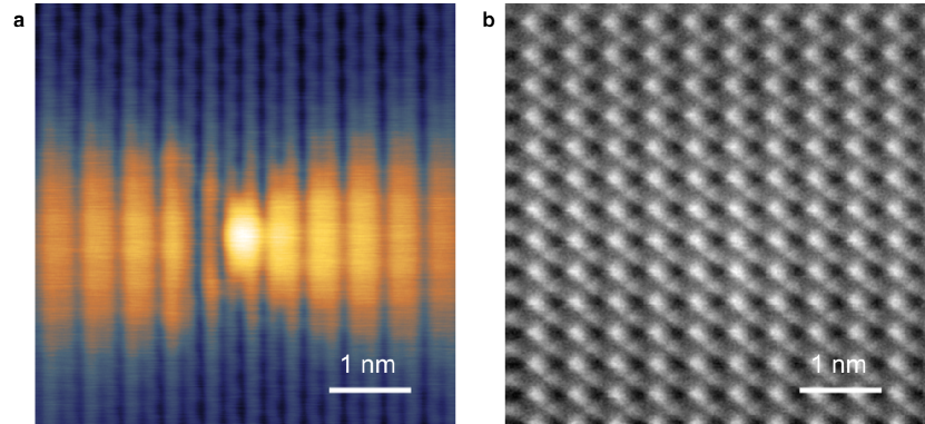
STM imaging of BP surface cleaved in-situ reveals a ubiquitous presence of defects with large-sized dumbbell-shaped appearance across more than tens of zigzag (ZZ) lattice chains (Fig. 1c), which are tentatively labeled as neutral SV (in the following context, SV represents neutral SV unless stated otherwise). The spatially extended dumbbell feature is probably associated with the delocalized bound hole states over SV due to its shallow acceptor nature, which will be further discussed in detail below. We also performed constant-height nc-AFM imaging of these defects with a CO-functionalized tip to monitor the spatial variation of frequency shift () in the Pauli repulsive regime. The higher reflects positions of atoms or chemical bond with a high electron density [37]. The nc-AFM image of SV shows the perfect ZZ chains attributed to the P atoms at the topmost surface (Fig. S5). This result suggests that these SVs reside in the sub-surface layers, consistent with a recent DFT prediction that SVs in the sub-surface layers are energetically more favorable [36].
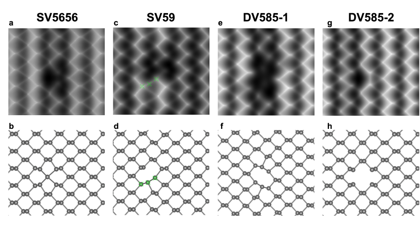
Upon thermal annealing at 453 K followed by rapid cooling, the majority of these dumbbell-shaped SVs vanished. Instead, a new type of defect manifested as a much smaller protrusion predominates the surface (Fig. 1d). A close examination revealed that this new defect adopts a butterfly-shaped feature spanning over two nearest neighbouring ZZ chains (Fig. 2a). Moreover, the identical STM contrast of these butterfly-shaped defects (BSDs) suggests that these surface feastures are due to the reconstruction and migration of SVs during thermal annealing.
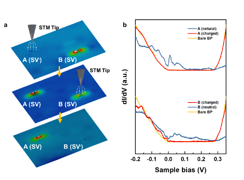
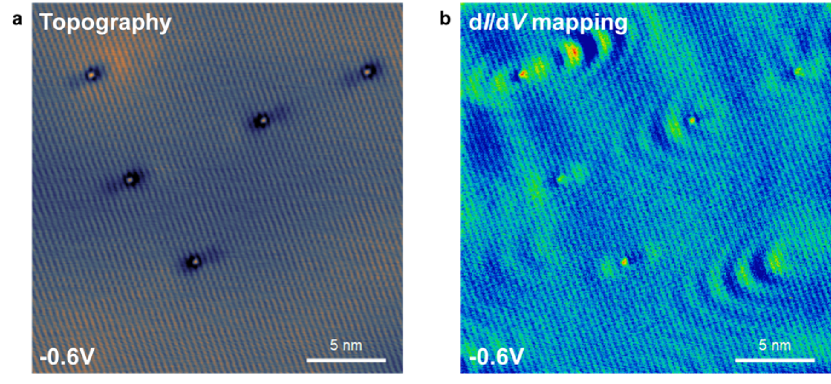
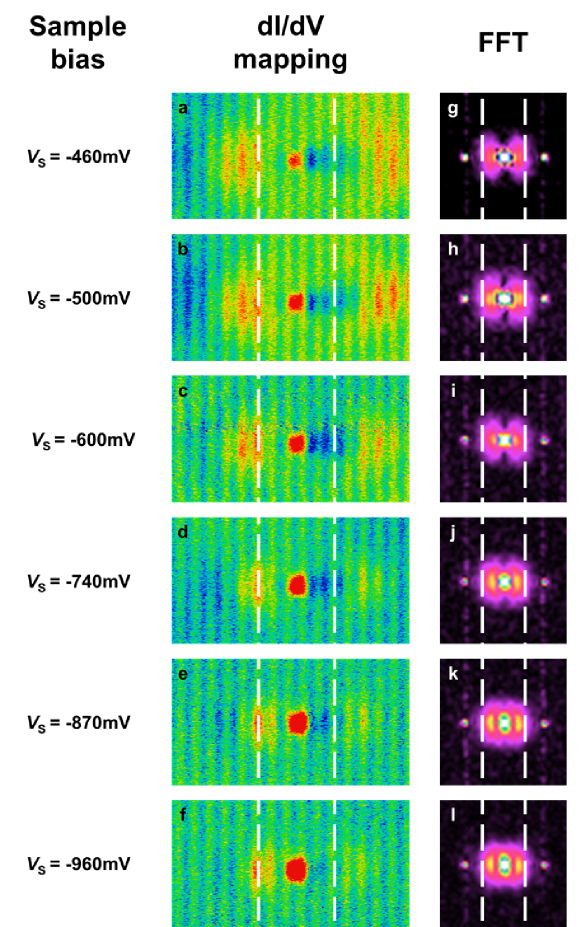
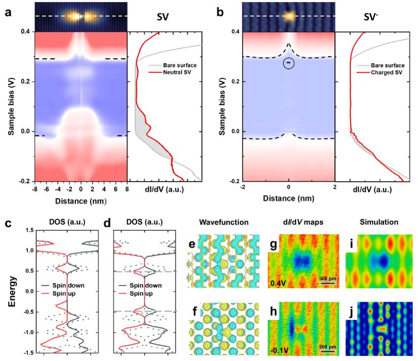
Bias-dependent line spectra taken across the dumbbell and butterfly defects along the armchair (AC) direction (indicated by a white dashed line) are shown in the left panel of Fig. 3a and 3b, respectively. A dumbbell-shaped SV mainly induces a strong LDOS modulation in the vicinity of the valence band maximum (VBM) as marked by grey color in the right panel of Fig. 3a. The in-gap states near VB of SV span nm away from the defect center, suggesting a shallow acceptor nature forming spatially extended bound hole states [38]. In contrast, BSD lacks in-gap states but exhibits an upward band bending of tens of meV for both VBM and CBM. In addition, maps taken at eV and eV show a weak modulation, including a faint dark depression and protrusion over the defect site, respectively (Fig. 3g,h). All these observations consistently show that BSD is negatively charged.
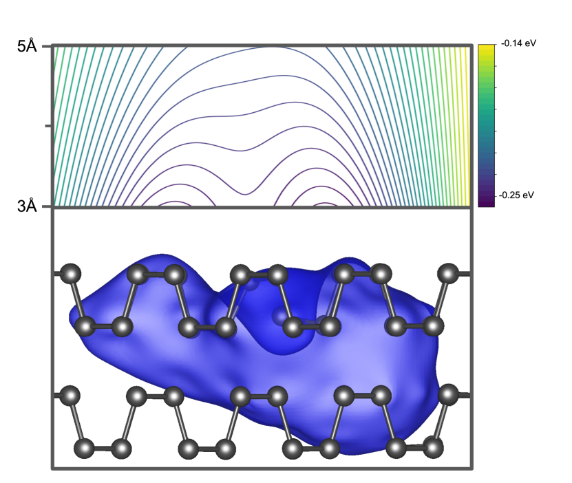
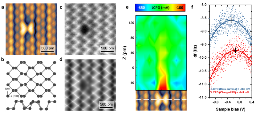
Kelvin probe force microscopy (KPFM) was further applied to characterize the local contact potential difference (LCPD) between BSD and bare BP surface. Fig. 2f presents the KPFM results acquired right over and nm away from BSD at a relative height of pm. A parabolic fitting of frequency shift curves reveals a positive shift of LCPD (i.e parabolic maximum) from mV (over bare BP) to mV (over BSD), conforming that BSDs are negatively charged [39]. The LCPD (, ) color-map acquired across BSD defect along the AC direction at different tip-sample distances further indicates a smaller LCPD and associated negative charge in close vicinity to BSD (Fig. 2e), consistent with the calculated potential profile (Fig. S6).
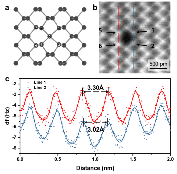
To decipher the local structure of BSD, we performed nc-AFM imaging with a CO-functionalized tip (Fig. 2c). The frequency shift image collected by nc-AFM reveals a dark hole-like feature surrounded by two bright spots and two dimmer spots. The protrusions in the nc-AFM image correspond to P atom positions due to their stronger repulsive interaction with CO-tip. Therefore, the nc-AFM image suggests BSD likely contains a missing top P atom (SV) or both top P and its bonded P atom at the bottom (divacancy denoted as DV). By DFT simulation of various defect structures via Probe Particle Model (See Fig. S3 in SI), the simulated nc-AFM (Fig. 2d) of reconstructed SV reproduces the key features in experimental data well, including bright asymmetric protrusions at two sides of BSD. Therefore, BSD is determined to be negatively charged SV (). The asymmetry in both STM and nc-AFM images of stems from the local reconstruction involving the bonding of central P atom with four adjacent P atoms (Fig. 2b and Fig. S4), forming a hypervalent configuration with one extra negative charge.
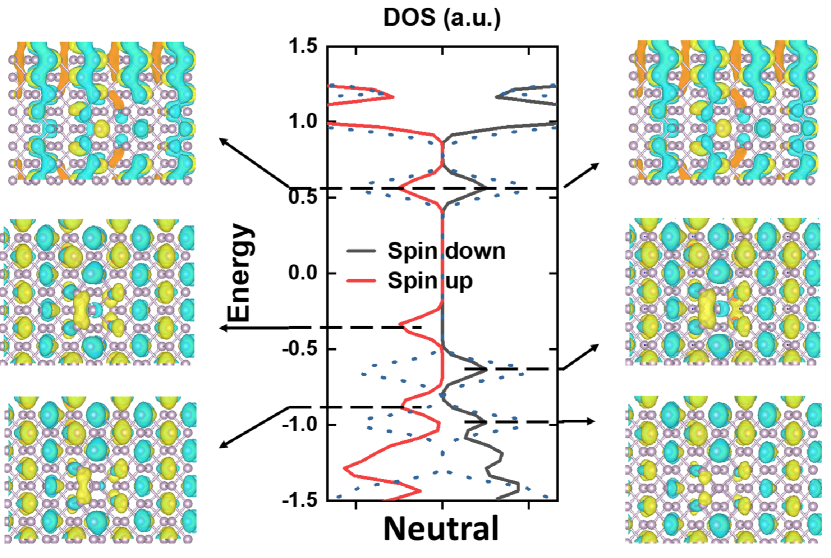
The drastically different electronic properties of neutral SV and can be further understood by DFT calculations using hybrid pbe0 functional. Neutral SV shows the spin-polarized density of states (DOS) with in-gap states above the VBM (Fig. 3c). In contrast, the calculated DOS of resembles that of pristine BP (dashed blue curve) with a slight shift of both VB and CB towards each other (Fig. 3d). Upon the local reconstruction and ionization of SV, all the DBs are passivated in , eliminating in-gap states and restoring the spin degeneracy in the DOS. Wavefunction plot of CB and VB band-edge states reveals a major contribution from dispersive band-like electronic states with small perturbation from the defect (Fig. 3e,f). In addition, the simulated maps at two energetic positions close to CB (Fig. 3i) and VB (Fig. 3j)side reproduce the key features in the experimental maps well. Therefore, a combination of DFT calculations and nc-AFM imaging unambiguously reveals that BSDs are , presumably transformed from neutral SV.
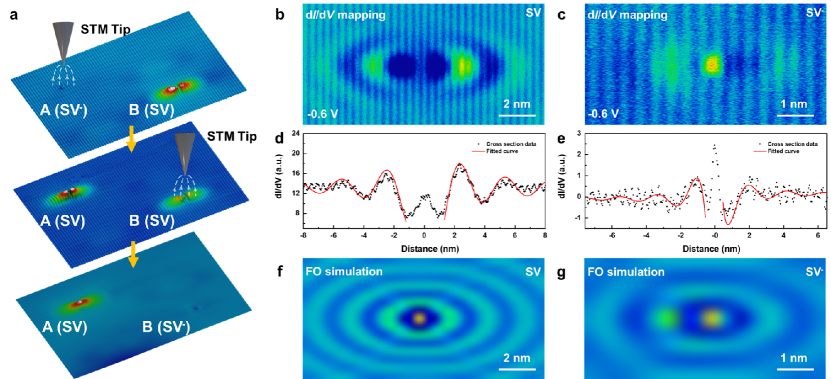
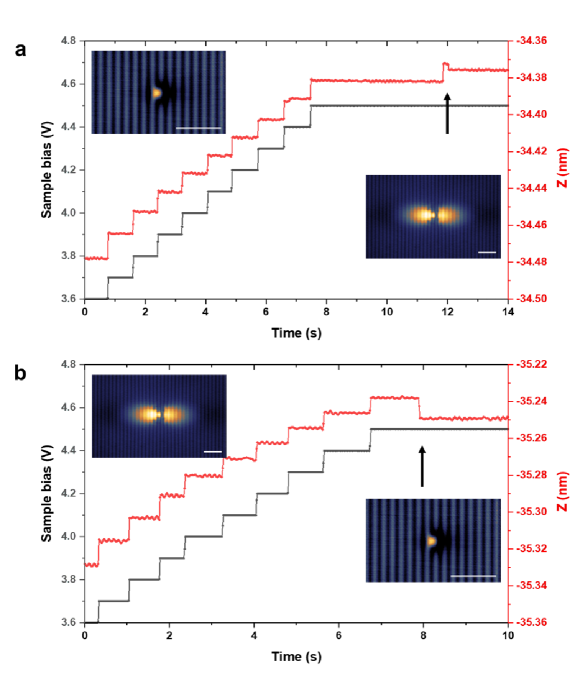
In addition, we took advantage of STM tip manipulation to control the switch between SV and over two individual defects as shown in Fig. 4a (from to SV for defect A and SV to for defect B). We note that a reversible switch over a single defect between SV and is challenging as high bias applied also may result in pulling nearby P atoms out from the surface, depending on the tip geometry. Nevertheless, positioning the STM tip over one charged defect A() followed by a gradual increase of sample bias to V, triggers its switch back to neutral SV with the re-emergence of characteristic dumbbell shape and in-gap states (Fig. S2). Similarly, upon applying a bias of V, another neutral B(SV) can be transformed into B() with the appearance of butterfly shape and disappearance of in-gap states (Fig. S2). Such a tip-controlled transformation between SV and is presumably attributed to the ionization and de-ionization of defects induced by the local electric field or inelastic tunnelling process [40, 41].
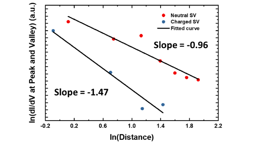
We then evaluated the impact of self-passivation of SV on the local charge scattering behavior by comparing the corresponding Friedel oscillations (FO) before and after ionization of SV. The scattering of charge carriers by defects often produces a periodic long-range modulation of the LDOS with periodicity associated with wave vector of scattered carriers [42]. We indeed observed contrasting LDOS oscillation pattern surrounding between SV and . The characteristic energy-dependent wavelength of these oscillation patterns verifies their FO origin (Fig. 4b-c and Fig. S9). Neutral SV exhibits a highly anisotropic FO pattern with a stronger modulation along the AC direction, which can be attributed to a smaller effective carrier mass along this crystallographic axis [43, 44]. According to the standard FO theory [45], we performed the fitting of the line cross-section data for both SV and to the expression: , which yields a dramatic difference in the phase, amplitude and decay rate of FO patterns between SV and . Firstly, the fitting of cross-section data to the equation above yields a phase difference between the oscillation at two sides of defect by for SV and for . Hence, a small phase shift at SV produces a nearly symmetric FO pattern, while a significant phase shift results in an asymmetric FO pattern across . Secondly, according to the fitting result, the oscillation amplitude in LDOS for SV (, ) is nearly one order of magnitude larger than that for (, ). Equally important, shows a faster decay rate () than SV (), which may be the result of a weak perturbation and a large phase shift between two sides of .
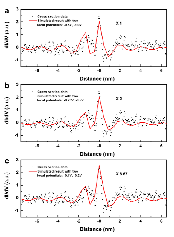
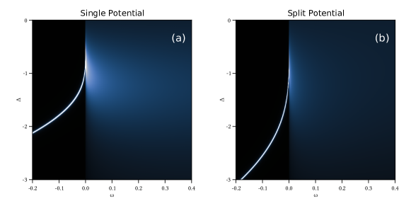
To understand the origin of different FO behaviours, we performed numerical calculations to simulate FO patterns for both SV and by treating BP as a single (valence) band 2D material with a direction-dependent carrier mass (See SI for details). Removing a P atom can be viewed as adding a P “anti-nucleus.” This negatively charged “anti-nucleus” creates an attractive long-range potential for the holes, giving rise to FO and mid-gap bound states, as seen in Fig. 3a and c. Although the potential profile is non-trivial and must include screening effects, it is illuminating to get a rough estimate of the energy scales involved by assuming that the perturbation is limited to the unit cell with the missing P atom. First, we note that the lowest-energy mid-gap state for SV is located about eV above the VBM. Next, following the approach described in SI, we calculate the spectral function for the unit cell hosting the vacancy for a range of attractive potentials generated by the “anti-nucleus,” as shown in Fig. S12. From our analysis, we observe that the single-unit-cell potential of about eV produces a localized state at the correct energy, which is thus set as the perturbation potential from SV to calculate the corresponding spectral maps of surrounding BP at different energies. The calculated spectral function map at the energy of eV reveals the symmetric oscillation pattern, consistent with experimental maps of SV taken at the same energy (Fig. 4b and f). The FO wavelength of nm in the AC direction obtained from the numerical simulations also agrees with the experimental results far from the defect (Fig. S8). As for , the local reconstruction involving the shift of central P atom to bond with adjacent four P atoms results in a more diffusive and asymmetric charge density, leading to a dipole-like potential splitting as shown in Fig. S6. To capture these effects, we split the perturbation ( eV) from SV into two unit cells. By adjusting the ratio and the separation (Fig. S11), we found that the calculated spectral function map with a split potential of and eV shows the best agreement with the experimental data (Fig. 4c). In fact, the asymmetry and phase shift of spectral function maps is independent on the absolute value of split potentials (Fig. S11). This points out that making the potential less singular by spreading the perturbation out spatially leads to a reduced band distortion and carrier scattering.
In summary, we demonstrated a new electronic self-passivation of SV in BP through the local reconstruction and ionisation of SV into negatively charged through a mild thermal annealing or STM tip manipulation, leading to the passivation of all the DBs and elimination of in-gap states. In contrast to SV with a strong and symmetric FO pattern, shows an asymmetric FO pattern with oscillation amplitude reduced by one order of magnitude and a faster decay rate, which can be attributed to its weak dipole-like perturbation. Our work opens up a new route for electronic self-passivation of defects, crucial for the further optimisation of the carrier mobility in BP and its analogues.
I Acknowledgements
J. Lu acknowledges the support from MOE grants (MOE2019-T2-2-044 and R-143-000-B58-114). M. Telychko acknowledges the support from A*STAR AME YIRG grant (Project No. A20E6c0098, R-143-000-B71-305). A.R. acknowledges the National Research Foundation, Prime Minister Office, Singapore, under its Medium Sized Centre Programme and the support by Yale-NUS College (through Grant No. R-607-265- 380-121). A.G. and P.J. acknowledge support of Czech Science Foundation project no. 20-13692X.
References
- Li et al. [2014] L. Li, Y. Yu, G. J. Ye, Q. Ge, X. Ou, H. Wu, D. Feng, X. H. Chen, and Y. Zhang, Nature Nanotechnol. 9, 372 (2014).
- Qiao et al. [2014] J. Qiao, X. Kong, Z. X. Hu, F. Yang, and W. Ji, Nat. Commun. 5, 4475 (2014).
- Buscema et al. [2014] M. Buscema, D. J. Groenendijk, S. I. Blanter, G. A. Steele, H. S. Van Der Zant, and A. Castellanos-Gomez, Nano Lett. 14, 3347 (2014).
- Chen et al. [2015] X. Chen, Y. Wu, Z. Wu, Y. Han, S. Xu, L. Wang, W. Ye, T. Han, Y. He, Y. Cai, and N. Wang, Nat. Commun. 6, 7315 (2015).
- Sheng et al. [2021] F. Sheng, C. Hua, M. Cheng, J. Hu, X. Sun, Q. Tao, H. Lu, Y. Lu, M. Zhong, K. Watanabe, T. Taniguchi, Q. Xia, Z.-A. Xu, and Y. Zheng, Nature 593, 56 (2021).
- Chen et al. [2008] J.-H. Chen, C. Jang, S. Xiao, M. Ishigami, and M. S. Fuhrer, Nature Nanotechnology 3, 206 (2008).
- Yu et al. [2014] Z. Yu, Y. Pan, Y. Shen, Z. Wang, Z. Y. Ong, T. Xu, R. Xin, L. Pan, B. Wang, L. Sun, J. Wang, G. Zhang, Y. W. Zhang, Y. Shi, and X. Wang, Nat. Commun. 5, 5290 (2014).
- Lin et al. [2015] Y. C. Lin, T. Björkman, H. P. Komsa, P. Y. Teng, C. H. Yeh, F. S. Huang, K. H. Lin, J. Jadczak, Y. S. Huang, P. W. Chiu, A. V. Krasheninnikov, and K. Suenaga, Nat. Commun. 6, 6736 (2015).
- Schuler et al. [2019] B. Schuler, D. Y. Qiu, S. Refaely-Abramson, C. Kastl, C. T. Chen, S. Barja, R. J. Koch, D. F. Ogletree, S. Aloni, A. M. Schwartzberg, J. B. Neaton, S. G. Louie, and A. Weber-Bargioni, Phys. Rev. Lett. 123, 076801 (2019).
- Liu et al. [2017] Y. Liu, Z. Qiu, A. Carvalho, Y. Bao, H. Xu, S. J. Tan, W. Liu, A. H. Castro Neto, K. P. Loh, and J. Lu, Nano Lett. 17, 1970 (2017).
- Kiraly et al. [2017] B. Kiraly, N. Hauptmann, A. N. Rudenko, M. I. Katsnelson, and A. A. Khajetoorians, Nano Lett. 17, 3607 (2017).
- Pashley et al. [1993] M. D. Pashley, K. W. Haberern, R. M. Feenstra, and P. D. Kirchner, Phys. Rev. B 48, 4612 (1993).
- Hong et al. [2015] J. Hong, Z. Hu, M. Probert, K. Li, D. Lv, X. Yang, L. Gu, N. Mao, Q. Feng, L. Xie, J. Zhang, D. Wu, Z. Zhang, C. Jin, W. Ji, X. Zhang, J. Yuan, and Z. Zhang, Nat. Commun. 6, 6293 (2015).
- Khan et al. [2017] M. A. Khan, M. Erementchouk, J. Hendrickson, and M. N. Leuenberger, Phys. Rev. B 95, 245435 (2017).
- Han et al. [2016] H. V. Han, A. Y. Lu, L. S. Lu, J. K. Huang, H. Li, C. L. Hsu, Y. C. Lin, M. H. Chiu, K. Suenaga, C. W. Chu, H. C. Kuo, W. H. Chang, L. J. Li, and Y. Shi, ACS Nano 10, 1454 (2016).
- Pak et al. [2015] J. Pak, J. Jang, K. Cho, T.-Y. Kim, J.-K. Kim, Y. Song, W.-K. Hong, M. Min, H. Lee, and T. Lee, Nanoscale 7, 18780 (2015).
- Park et al. [2017] J. H. Park, A. Sanne, Y. Guo, M. Amani, K. Zhang, H. C. Movva, J. A. Robinson, A. Javey, J. Robertson, S. K. Banerjee, and A. C. Kummel, Sci. Adv. 3, e1701661 (2017).
- Amani et al. [2015] M. Amani, D.-H. Lien, D. Kiriya, J. Xiao, A. Azcatl, J. Noh, S. R. Madhvapathy, R. Addou, S. KC, M. Dubey, K. Cho, R. M. Wallace, S.-C. Lee, J.-H. He, J. W. Ager, X. Zhang, E. Yablonovitch, and A. Javey, Science 350, 1065 (2015).
- Cho et al. [2015] K. Cho, M. Min, T.-Y. Kim, H. Jeong, J. Pak, J.-K. Kim, J. Jang, S. J. Yun, Y. H. Lee, W.-K. Hong, and T. Lee, ACS Nano 9, 8044 (2015), pMID: 26262556.
- Luo et al. [2015] Z. Luo, J. Maassen, Y. Deng, Y. Du, R. P. Garrelts, M. S. Lundstrom, P. D. Ye, and X. Xu, Nat. Commun. 6, 8572 (2015).
- Li et al. [2015] L. Li, G. J. Ye, V. Tran, R. Fei, G. Chen, H. Wang, J. Wang, K. Watanabe, T. Taniguchi, L. Yang, X. H. Chen, and Y. Zhang, Nature Nanotechnology 10, 608 (2015).
- Deng et al. [2017] B. Deng, V. Tran, Y. Xie, H. Jiang, C. Li, Q. Guo, X. Wang, H. Tian, S. J. Koester, H. Wang, J. J. Cha, Q. Xia, L. Yang, and F. Xia, Nat. Commun. 8, 14474 (2017).
- Li et al. [2017] L. Li, J. Kim, C. Jin, G. J. Ye, D. Y. Qiu, F. H. Da Jornada, Z. Shi, L. Chen, Z. Zhang, F. Yang, K. Watanabe, T. Taniguchi, W. Ren, S. G. Louie, X. H. Chen, Y. Zhang, and F. Wang, Nature Nanotechnol. 12, 21 (2017).
- Jung et al. [2020] S. W. Jung, S. H. Ryu, W. J. Shin, Y. Sohn, M. Huh, R. J. Koch, C. Jozwiak, E. Rotenberg, A. Bostwick, and K. S. Kim, Nat. Mater. 19, 277 (2020).
- Xia et al. [2014] F. Xia, H. Wang, and Y. Jia, Nat. Commun. 5, 4458 (2014).
- Wang et al. [2015] X. Wang, A. M. Jones, K. L. Seyler, V. Tran, Y. Jia, H. Zhao, H. Wang, L. Yang, X. Xu, and F. Xia, Nature Nanotechnol. 10, 517 (2015).
- Liu et al. [2016] Y. Liu, T. Low, and P. P. Ruden, Phys. Rev. B 93, 165402 (2016).
- Riffle et al. [2018] J. V. Riffle, C. Flynn, B. St Laurent, C. A. Ayotte, C. A. Caputo, and S. M. Hollen, J. Appl. Phys. 123, 044301 (2018).
- Babar and Kabir [2019] R. Babar and M. Kabir, Phys. Rev. Mater. 3, 074008 (2019).
- Cai et al. [2016] Y. Cai, Q. Ke, G. Zhang, B. I. Yakobson, and Y.-W. Zhang, Journal of the American Chemical Society 138, 10199 (2016), pMID: 27448591.
- Yao et al. [2020] F. Yao, Y. Cai, Z. Xiao, G. Zhang, R.-J. Xie, and C. Jin, 2D Materials 8, 025004 (2020).
- Liu et al. [2014] Y. Liu, F. Xu, Z. Zhang, E. S. Penev, and B. I. Yakobson, Nano Lett. 14, 6782 (2014).
- Guo and Robertson [2015] Y. Guo and J. Robertson, Sci. Rep. 5, 14165 (2015).
- Hu and Dong [2015] T. Hu and J. Dong, Nanotechnology 26, 65705 (2015).
- Hu and Yang [2015] W. Hu and J. Yang, J. Phys. Chem. C 119, 20474 (2015).
- Gaberle and Shluger [2018] J. Gaberle and A. L. Shluger, Nanoscale 10, 19536 (2018).
- Gross et al. [2009a] L. Gross, F. Mohn, N. Moll, P. Liljeroth, and G. Meyer, Science 325, 1110 (2009a).
- Qiu et al. [2017] Z. Qiu, H. Fang, A. Carvalho, A. S. Rodin, Y. Liu, S. J. Tan, M. Telychko, P. Lv, J. Su, Y. Wang, A. H. Castro Neto, and J. Lu, Nano Lett. 17, 6935 (2017).
- Gross et al. [2009b] L. Gross, F. Mohn, P. Liljeroth, J. Repp, F. J. Giessible, and G. Meyer, Science 324, 1428 (2009b).
- Lee and Gupta [2010] D. H. Lee and J. A. Gupta, Science 330, 1807 (2010).
- Wong et al. [2015] D. Wong, J. Velasco, L. Ju, J. Lee, S. Kahn, H. Z. Tsai, C. Germany, T. Taniguchi, K. Watanabe, A. Zettl, F. Wang, and M. F. Crommie, Nature Nanotechnol. 10, 949 (2015).
- Friedel [1952] J. Friedel, The London, Edinburgh, and Dublin Philosophical Magazine and Journal of Science 43, 153 (1952).
- Zou et al. [2016] Y. L. Zou, J. Song, C. Bai, and K. Chang, Phys. Rev. B 94, 035431 (2016).
- Kiraly et al. [2019] B. Kiraly, E. J. Knol, K. Volckaert, D. Biswas, A. N. Rudenko, D. A. Prishchenko, V. G. Mazurenko, M. I. Katsnelson, P. Hofmann, D. Wegner, and A. A. Khajetoorians, Phys. Rev. Lett. 123, 216403 (2019).
- Crommie et al. [1993] M. F. Crommie, C. P. Lutz, and D. M. Eigler, Nature 363, 524 (1993).
- Blum et al. [2009] V. Blum, R. Gehrke, F. Hanke, P. Havu, V. Havu, X. Ren, K. Reuter, and M. Scheffler, Computer Physics Communications 180, 2175 (2009).
- Ren et al. [2012] X. Ren, P. Rinke, V. Blum, J. Wieferink, A. Tkatchenko, A. Sanfilippo, K. Reuter, and M. Scheffler, New Journal of Physics 14, 053020 (2012).
- Tkatchenko and Scheffler [2009] A. Tkatchenko and M. Scheffler, Phys. Rev. Lett. 102, 073005 (2009).
- Hultgren et al. [1935] R. Hultgren, N. S. Gingrich, and B. E. Warren, The Journal of Chemical Physics 3, 351 (1935).
- Lewis et al. [2011] J. P. Lewis, P. Jelínek, J. Ortega, A. A. Demkov, D. G. Trabada, B. Haycock, H. Wang, G. Adams, J. K. Tomfohr, E. Abad, H. Wang, and D. A. Drabold, physica status solidi (b) 248, 1989 (2011).
- Lee et al. [1988] C. Lee, W. Yang, and R. G. Parr, Phys. Rev. B 37, 785 (1988).
- Grimme et al. [2010] S. Grimme, J. Antony, S. Ehrlich, and H. Krieg, The Journal of Chemical Physics 132, 154104 (2010).
- Hapala et al. [2014] P. Hapala, G. Kichin, C. Wagner, F. S. Tautz, R. Temirov, and P. Jelínek, Phys. Rev. B 90, 085421 (2014).
- Krejčí et al. [2017] O. Krejčí, P. Hapala, M. Ondráček, and P. Jelínek, Phys. Rev. B 95, 045407 (2017).
- Bezanson et al. [2017] J. Bezanson, A. Edelman, S. Karpinski, and V. B. Shah, Society for Industrial and Applied Mathematics 59, 10.1137/141000671 (2017).
II Supplementary Information
Appendix A Sample preparation
The bulk BP crystal (HQ graphene) was cleaved under ultrahigh vacuum to remove the degraded surface. Subsequently, the sample was heated up to 375 K to further remove potential absorbents before conducting the STM imaging and STS spectroscopic measurements at 4.8 K using Createc LT-STM system. The tungsten tip was calibrated spectroscopically to check the Shockley surface state on Au (111) surface. All the spectroscopy and mapping were obtained by a standard lock-in technique with a modulation voltage of 10mV and modulation frequency of 877Hz.
Appendix B DFT and Simulated SPM methods.
All the studied structures were relaxed with the FHI-AIMS [46] package using the hybrid pbe0 [47] potential with light wave functions and spin treatment, using the -point to describe the reciprocal space. Van der Waals interaction was included using the Tkatchenko–Scheffler approximation [48] and we set a tolerance for the convergence of force and energy of eV/Å and eV, respectively. For the calculations, we used a 4-layers supercell of black phosphorus formed by 256 atoms (255 for the SV and 254 for the DV structures) of phosphorus, allowing the 3 top layers to relax with Å of vacuum space above and lattice constants Å and Å[49]. After the simulations with AIMS, a supercell composed by 2303 atoms of the SV structure was built and studied for both neutral and charged state. The 5.25 nm (armchair) and 3.98 nm (zig-zag) distances between the vacancy and its periodic copies isolate it and allow us to study the large scale charge redistribution shown in Fig. S6. To study this rather large system we used the home build code Fireball [50] using the general gradient approximation BLYP [51] and vdW-D3[52] with a local-orbital basis set with a.u., a.u. and a.u.. To check the precision of the fireball calculations we replicated the calculation carried with AIMS of the supercell of the SV structure and obtained similar wavefunctions in shape and order. The simulated AFM images were obtained with the probe particle model package [53] using a stiffness of and a factor for the electrostatic interaction included using the hartree potential of black phosphorus calculated with DFT. Simulated images were obtained with the PP-STM code [54], using a s-like orbital as probe and the eigenstates from AIMS to describe the sample.
Appendix C Friedel oscillation fitting
The cross-section data of FO can be divided into three parts: FO pattern on the left, the LDOS modulation by defect state at center, and FO pattern on the right. These three parts can be fitted and understood respectively: the defect state follows the Gaussian distribution along AC direction; the FO patterns on both sides are fitted by the expression for LDOS oscillations as a function of distance : [45]
| (1) |
where is the initial amplitude, is the independent variable, is the center position determined by extracting the peak center at defect state, is the wavelength determined from the FFT results, is the phase of FO, is the decay rate determined by fitting the peak and valley intensity to distance in logarithm scale, is a constant value from the background.
Appendix D Analytical Formalism
To describe the pristine BP with added local potential, we use the single-band nearly-free electron model with a direction-dependent dispersion , where is the electron mass, while and are the effective masses in arm-chair and zigzag directions. Note that 0.15 in the AC direction and 1.18 in the ZZ direction, where is the electron rest mass. [2]). the single-band model contains one orbital per unit cell, setting the limit for the finest resolution scale.
The second-quantized Hamiltonian for the system can be written as
| (2) |
Here, () are fermionic creation (annihilation) operators for the single-band eigenstates, () are their real-space counterparts operating on the unit cell at , and is the position-dependent potential. To write the summation as matrix product, we combine and into vectors of operators and , respectively. () is a diagonal matrix with () on the diagonal.
Using the fact that and are related by the Fourier transform, we have , where the elements of the matrix are given by and is the number of unit cells in the system. With this, the Hamiltonian can be rewritten using the real-space operators as
| (3) |
Next, we use this Hamiltonian to obtain the real-space Matsubara Green’s function by subtracting the matrix in Eq. (3) from and taking the inverse:
| (4) |
Here, is the real-space Green’s function for the unperturbed system and the last term in the expression above is the correction due to .
We can obtain the spectral function by taking the diagonal elements of the Green’s function and substituting with
| (5) |
where is measured relative to the Fermi level. Given that is diagonal and only contains non-zero entries for the unit cells containing the local potential, the expression inside the brackets simplifies to
| (6) |
where only contains the unit cells where local potential is added and is the portion of including only these unit cells.
To calculate , first note that is a unitary matrix so that
| (7) |
The matrix elements of are given by
| (8) |
where we used the fact that is a diagonal matrix. Changing the momentum sum into an integral yields
| (9) |
where is the area of the system, is the area of the unit cell, and .
For ,
| (10) |
where is the modified Bessel function. When , we need to introduce a cutoff so that the integral does not diverge
| (11) |
We now consider the choice of . Recall that is the spectral function for the pristine system whose integral over the energies , yields . Using this fact, we have
| (12) |
leading to
| (13) |
where , is the Rydberg energy, and is the Bohr radius. Finally, is given by
| (14) | ||||
| (15) |
All the field-theoretic numerical calculations were performed using Julia programming language. [55] The code is available at https://github.com/rodin-physics/black-phosphorus-defects.