Activation of magnetic moments in CVD-grown graphene by annealing
Abstract
Effects of annealing on chemical vapor deposited graphene are investigated via a weak localization magnetoresistance measurement. Annealing at in inert gases, a common cleaning procedure for graphene devices lin2011graphene ; cheng2011toward , is found to raise the dephasing rate significantly above the rate from electron-electron interactions, which would otherwise be expected to dominate dephasing at 4 K and below PhysRevB.22.5142 ; kozikov2010electron ; tikhonenko2008weak ; tikhonenko2009transition ; min2017asymmetric . This extra dephasing is apparently induced by local magnetic moments activated by the annealing process, and depends strongly on the backgate voltage applied.
I I. Introduction
The first graphene samples made into electronic devices came from flakes exfoliated from bulk graphite, and were only a few microns in size neto2009electronic ; geim2010rise . The discovery that graphene could also be grown over large areas, using a chemical vapour deposition (CVD) process on metal films, opened up many technological possibilities that were unimaginable with exfoliated flakes. One application proposed in the early days of graphene research was spintronics, making use of potentially long spin lifetimes in carbon-based materials. Although the hope of graphene spintronics persists, experimental realizations remain less impressive than theoretical proposals RevModPhys.92.021003 ; han2011spin .
Despite the promise of CVD-grown graphene for technology, this growth technique tends to yield samples with more defects, such as carbon vacancies and domain boundaries, compared to exfoliated graphene lee2017review . In fact, defects like those found in CVD graphene are believed to be a potential source of magnetic moments that would spoil spintronic applicationsyazyev2007defect . At the same time, the interaction of magnetic moments with conduction electrons in graphene is predicted to be different than what is observed in conventional metals, offering new avenues to realize correlated electronic statesshi2019kondo .
Here, we present an unexpected characteristic of defects in CVD graphene: we show that the relatively gentle annealing process typically used to remove residues from graphene devices lin2011graphene ; ishigami2007atomic ; dan2009intrinsic ; cheng2011toward ; pirkle2011effect ; dean2010boron ; leong2014does ; lin2012graphene significantly enhances the quantum mechanical phase-breaking (dephasing) rate measured via weak localization (WL)tikhonenko2008weak , and that this dephasing is due to the activation of magnetic moments. Although data from phase coherent measurements at cryogenic temperatures might seem unrelated to applications at room temperature, our results imply that these activated defects create a fast mechanism for spin relaxation that would limit the use of CVD graphene in spintronics. At the same time, this finding sheds light on the microscopic origin of local moments in this form of graphene, and demonstrates that samples grown by CVD will be a fruitful platform to study interactions between magnetic moments and electrons in graphene.
II II. Experimental methods
Multiple samples were prepared by transferring commercial CVD graphene (ACS Materials Co., MA) onto n-doped Si wafers with a 295 nm SiOx dielectric. In some samples, a 30 nm HfO2 film was grown by atomic layer deposition (ALD) at on the SiOx before transferring graphene [Fig. S1 inset]. Hall bars with a width and a length of 30 m by 30 m were defined by electron beam lithography. Cr/Au (5/80nm) ohmic contacts were used to apply a bias current, , and measure longitudinal and transverse voltages, and [Fig. 1(a)], then was converted into resistivity or conductivity using the geometric aspect ratio of the Hall bar. The carrier density, , was tuned using the backgate voltage, , and measured via low-field Hall effect.
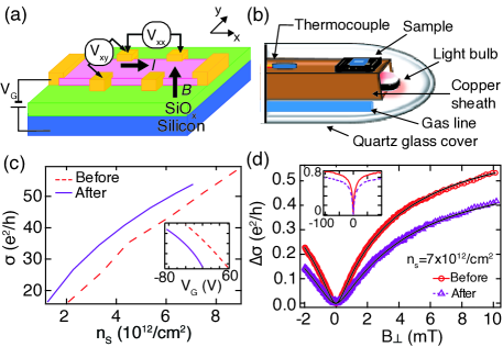
Annealing was performed in Ar, N2, forming gas (5% H2/95% N2, hereafter H2/N2), or under vacuum, using a simple thermal annealer [Fig. 1(b)]. Samples wire-bonded into ceramic chip carriers were loaded into the annealer, then pumped to a base pressure of mbar (gas anneal) or mbar (vacuum anneal). For gas annealing, the chamber was pumped-and-flushed, then the flow rate adjusted using a needle valve until a pressure of 200 mbar was attained. Samples were annealed for 1 hour at , then cooled to room temperature in the same atmosphere as the annealing step, and immediately transferred to the cryostat. After evacuating the cryostat and adding He exchange gas, samples were cooled to 4.2 K for measurement. The total air exposure time after annealing was less than one minute.
III III. Result and discussion
Figure 1(c) compares of a sample before and after annealing in Ar. The conductivity itself rose slightly, while the gate voltage required to reach the charge neutrality point, , decreased from 88 V to 18 V. The quantum correction to the perpendicular magnetoconductivity, , also changed after annealing [Fig. 1(d)]. To interpret this change, phase () and intervalley () scattering rates were extracted from using fits to the standard WL expression for graphene mccann2006weak ; tikhonenko2008weak ,
| (1) |
where , , diffusion constant and m/s for graphene. A third term reflecting intravalley scattering is omitted here for clarity as it did not affect the extracted or , but was included in the fitting supple .
Both and rose due to annealing. The rise in reflects increased short-range scattering due to changes in the interaction between graphene and SiOx dielectric, caused by the annealing itself cheng2011toward . The significant rise in is more surprising, and is the central focus of this work.
Electron-electron (e-e) and electron-phonon (e-p) interactions are well known dephasing mechanisms in metallic systems. Below 50 K in graphene the e-e rate dominates, and at 4 K the e-p rate is negligible in comparison tikhonenko2008weak ; tikhonenko2009transition ; min2017asymmetric . The e-e dephasing rate in graphene is Altshuler_1982 ; aleiner1999interaction ; mccann2006weak ; tikhonenko2008weak ; min2017asymmetric :
| (2) |
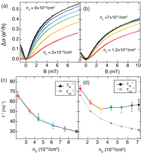
For the data in Fig. 1(d), Eq. 2 predicts = 33 ns-1 before annealing, matching the measured value =332 ns-1. After annealing, the calculated value from Eq. 2 is barely changed, = 32 ns-1, but the measured value rises to =605 ns-1. Fig. 2 extends this analysis to a range of . Before annealing, measured coincide almost exactly with calculated [Fig. 2(c)]. After annealing, on the other hand, exceeds everywhere, with the difference, , growing larger with [Fig. 2(d)]. Taken together, Figs. 2(c) and 2(d) indicate that e-e interaction dominates dephasing in samples as deposited, but new interactions emerge in Ar-annealed samples that add 10’s of ns-1 of excess dephasing.
As an inert gas, Ar is not expected to create chemical modifications to graphene at temperatures of only a few hundred ∘C. Indeed, transmission electron microscope investigations have confirmed that anneals such as those performed here do not affect perfect graphene, but that polymer resist and other residues begin to break down in the 150 to 250 ∘C temperature range, and radicals formed during that process may interact with dangling bonds at graphene defect sites lin2012graphene . Our observations are consistent with the reports of Ref. lin2012graphene, , that the influence of annealing on defect activation is via the thermal decomposition of residues rather than the gas itself.
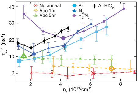
Figure 3 compiles the excess dephasing rate, , for a variety of annealing recipes, and leads to several observations. When annealing is performed in vacuum, is very small, rising only to 10 ns-1 (constant in ) even after 5 hours of annealing. For anneals in a gas environment, is significantly larger, growing with by an amount that does not depend on the choice of gas. also increases at low , most noticeably for samples annealed in H2/N2 .
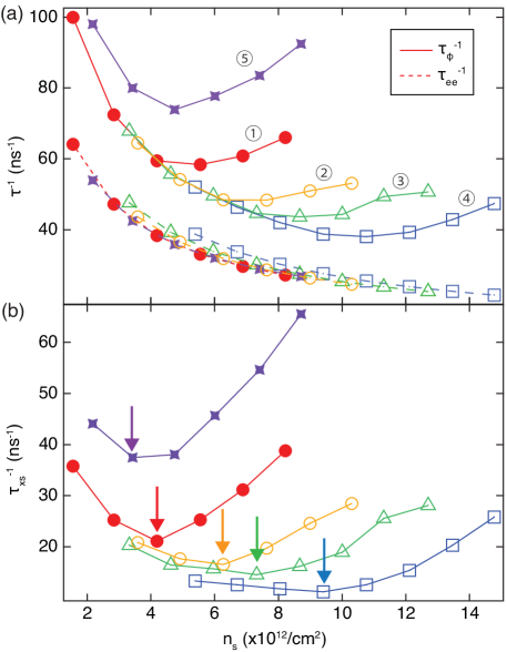
Upon closer examination, the rise in at low in the H2/N2 -annealed data from Fig. 3a appears to be related to the gate voltage applied, rather than specifically to the reduction in carrier density, with the minimum in consistently occurring at . The charge neutrality point, , was much larger for H2/N2 (=60 V) compared to Ar (=18 V) or N2 (=31 V), so larger negative was applied to H2/N2 -annealed samples to reach the low density regime. Further insight into the importance of , independent of , is gained by measuring the -dependent dephasing rate for a particular annealed sample, repeatedly shifting the Dirac point through exposure to ambient atmosphere [Fig. 4] C0JM02922J . ① represents for the sample immediately after an hour of annealing in H2/N2 (=60 V), ②-④ represent subsequent one hour exposures to ambient atmosphere (=92,109,140 V), then ⑤ represents an additional one hour anneal in H2/N2 (=70 V). Calculated for the different exposures fall along a single curve [Fig. 4(a)], reflecting the fact that does not change through these different steps. Measured also fall along a single curve for the low- part of each scan, for ①-④. However, the onset of the upturn in at high shifts to higher and higher densities with exposure to air, while the minimum in remains pinned to [arrows in Fig. 4(b)]. This seems to indicate that the upturns in and at high density are connected to the electric field between the graphene and the backgate rather than to the carrier density itself.
The persistent upturn in at large (strongly negative ), even after extended exposure to air, indicates that the activation of a dephasing mechanism by annealing is robust. A second annealing step (⑤) following the multiple exposures to air results in shifting back to 70 V, while increases above even the values observed after the first anneal (①). As was the case for ①-④, the minimum in remains at .
Just as the activated dephasing mechanism does not seem to depend on the choice of annealing gas, it also does not depend on the substrate. In order to test for a possible influence from the substrate van2016spin ; chen2012electronic ; scarfe2021systematic ; poljak2013influence , Fig. 3 includes data from a sample, annealed in Ar gas, on a wafer where ALD-grown HfO2 covers the SiOx [Fig. S1 inset]. HfO2 layers are amorphous when grown at the low temperatures used here, presumably with a defect density and type different from those found in thermal silicon oxide hausmann2003surface . The mobility of the HfO2 sample was similar to the samples on SiOx, in contrast to previous reports of mobility enhancement by screening due to high- dielectricschen2009dielectric ; konar2010effect ; this may indicate that the mobility in our samples is limited by defects in the graphene rather than charged-impurity scattering. More importantly, the measured for the HfO2 sample is nearly identical to that of the SiOx sample supple . From this, we tentatively conclude that the defects relevant to the dephasing enhancement lie in or on the graphene itself, rather than in the substrate.
The role of annealing temperature was also explored (data not shown). Below , annealing had minimal effect on for any of the inert gases. At the effect was similar to, though less strong than, the data shown here. For anneals at and above, the excess dephasing was even larger but the graphene mobility was degraded.
IV IV. dephasing mechanism
The effect of an in-plane magnetic field on WL can reveal spin-related mechanisms for dephasing. Magnetic fields, , applied in the plane of a graphene sheet influence in two ways. First, ripples in the graphene create an out-of-plane local magnetic field, fluctuating randomly across the graphene even when is applied exactly along the average plane of the sample. These out-of-plane components break time reversal symmetry locally, yielding an additional dephasing mechanism that grows quadratically with lundeberg2010rippled . Second, aligns local magnetic moments with Lande g-factor once . When free to rotate, these moments contribute to dephasing through spin flip scattering of conduction electrons, but that mechanism is suppressed when the moments are aligned by lundeberg2010rippled ; lundeberg2013defect ; kochan2014spin .
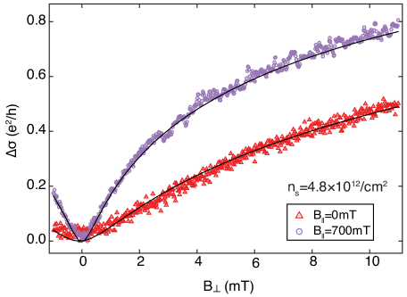
Cooling the graphene samples in a dilution refrigerator equipped with a two-axis magnet enabled measurements with finite , at temperatures low enough that spins could be aligned by before dephasing due to ripples was significant. Fig. 5 shows WL data for an H2/N2-annealed sample at 100 mK. (This sample was annealed at to maximize .) The lineshape of changes when in-plane field is applied, and fits to Eq. 1 confirm that drops from 95 ns-1 (=0) to 24 ns-1 at =0.7 T, where with =2. Ripples would have induced the opposite effect (increased for higher ). This data shows that spin flips induced by magnetic moments are the predominant mechanism for excess dephasing after annealing, contributing at least 70 ns-1.
Magnetic moments are believed to emerge at graphene defects, including vacancies yazyev2007defect ; chen2014magnetic , impurities han2011spin ; jozsa2009linear , and strain fluctuations couto2014random ; neumann2015raman . In most cases, the interactions of defect-bound moments with conduction electrons are predicted to strengthen at low carrier density due to weaker screening chen2014magnetic ; haase2011magnetic ; yazyev2007defect ; engels2014limitations . We find, in contrast, that increases at higher and, more importantly, depends more on the electric field due to than on the carrier density itself since gas annealed samples show the minimum near =0. It may be, therefore, that the magnetic moments being activated by gas annealing are of a different type than has been previously reported in experiment or studied theoretically.
References
- [1] Yung-Chang Lin, Chun-Chieh Lu, Chao-Huei Yeh, Chuanhong Jin, Kazu Suenaga, and Po-Wen Chiu. Graphene annealing: how clean can it be? Nano letters, 12(1):414–419, 2011.
- [2] Zengguang Cheng, Qiaoyu Zhou, Chenxuan Wang, Qiang Li, Chen Wang, and Ying Fang. Toward intrinsic graphene surfaces: a systematic study on thermal annealing and wet-chemical treatment of sio2-supported graphene devices. Nano letters, 11(2):767–771, 2011.
- [3] B. L. Altshuler, D. Khmel’nitzkii, A. I. Larkin, and P. A. Lee. Magnetoresistance and hall effect in a disordered two-dimensional electron gas. Phys. Rev. B, 22:5142–5153, Dec 1980.
- [4] AA Kozikov, AK Savchenko, BN Narozhny, and AV Shytov. Electron-electron interactions in the conductivity of graphene. Physical Review B, 82(7):075424, 2010.
- [5] FV Tikhonenko, DW Horsell, RV Gorbachev, and AK Savchenko. Weak localization in graphene flakes. Physical review letters, 100(5):056802, 2008.
- [6] FV Tikhonenko, AA Kozikov, AK Savchenko, and RV Gorbachev. Transition between electron localization and antilocalization in graphene. Physical Review Letters, 103(22):226801, 2009.
- [7] Kil-Joon Min, Jaesung Park, Wan-Seop Kim, and Dong-Hun Chae. Asymmetric electron-hole decoherence in ion-gated epitaxial graphene. Scientific reports, 7(1):1–7, 2017.
- [8] AH Castro Neto, Francisco Guinea, Nuno MR Peres, Kostya S Novoselov, and Andre K Geim. The electronic properties of graphene. Reviews of modern physics, 81(1):109, 2009.
- [9] Andre K Geim and Konstantin S Novoselov. The rise of graphene. In Nanoscience and technology: a collection of reviews from nature journals, pages 11–19. World Scientific, 2010.
- [10] A. Avsar, H. Ochoa, F. Guinea, B. Özyilmaz, B. J. van Wees, and I. J. Vera-Marun. Colloquium: Spintronics in graphene and other two-dimensional materials. Rev. Mod. Phys., 92:021003, Jun 2020.
- [11] Wei Han and Roland K Kawakami. Spin relaxation in single-layer and bilayer graphene. Physical review letters, 107(4):047207, 2011.
- [12] H Cheun Lee, Wei-Wen Liu, Siang-Piao Chai, Abdul Rahman Mohamed, Azizan Aziz, Cheng-Seong Khe, N MS Hidayah, and U Hashim. Review of the synthesis, transfer, characterization and growth mechanisms of single and multilayer graphene. RSC advances, 7(26):15644–15693, 2017.
- [13] Oleg V Yazyev and Lothar Helm. Defect-induced magnetism in graphene. Physical Review B, 75(12):125408, 2007.
- [14] Zheng Shi, Emilian M Nica, and Ian Affleck. Kondo effect due to a hydrogen impurity in graphene: a multichannel kondo problem with diverging hybridization. Physical Review B, 100(12):125158, 2019.
- [15] Masa Ishigami, JH Chen, WG Cullen, MS Fuhrer, and ED Williams. Atomic structure of graphene on sio2. Nano letters, 7(6):1643–1648, 2007.
- [16] Yaping Dan, Ye Lu, Nicholas J Kybert, Zhengtang Luo, and AT Charlie Johnson. Intrinsic response of graphene vapor sensors. Nano letters, 9(4):1472–1475, 2009.
- [17] A Pirkle, J Chan, A Venugopal, D Hinojos, CW Magnuson, S McDonnell, L Colombo, EM Vogel, RS Ruoff, and RM Wallace. The effect of chemical residues on the physical and electrical properties of chemical vapor deposited graphene transferred to sio2. Applied Physics Letters, 99(12):122108, 2011.
- [18] Cory R Dean, Andrea F Young, Inanc Meric, Chris Lee, Lei Wang, Sebastian Sorgenfrei, Kenji Watanabe, Takashi Taniguchi, Phillip Kim, Kenneth L Shepard, et al. Boron nitride substrates for high-quality graphene electronics. Nature nanotechnology, 5(10):722–726, 2010.
- [19] Wei Sun Leong, Chang Tai Nai, and John TL Thong. What does annealing do to metal–graphene contacts? Nano letters, 14(7):3840–3847, 2014.
- [20] Yung-Chang Lin, Chun-Chieh Lu, Chao-Huei Yeh, Chuanhong Jin, Kazu Suenaga, and Po-Wen Chiu. Graphene annealing: how clean can it be? Nano letters, 12(1):414–419, 2012.
- [21] See supplemental material at [url will be inserted by publisher] for further details on the experiment.
- [22] Edward McCann, K Kechedzhi, Vladimir I Fal’ko, H Suzuura, T Ando, and BL Altshuler. Weak-localization magnetoresistance and valley symmetry in graphene. Physical Review Letters, 97(14):146805, 2006.
- [23] B L Altshuler, A G Aronov, and D E Khmelnitsky. Effects of electron-electron collisions with small energy transfers on quantum localisation. Journal of Physics C: Solid State Physics, 15(36):7367–7386, dec 1982.
- [24] IL Aleiner, BL Altshuler, and ME Gershenson. Interaction effects and phase relaxation in disordered systems. Waves in Random Media, 9(2):201–240, 1999.
- [25] Hongtao Liu, Yunqi Liu, and Daoben Zhu. Chemical doping of graphene. J. Mater. Chem., 21:3335–3345, 2011.
- [26] JJ Van Den Berg, Rositsa Yakimova, and BJ Van Wees. Spin transport in epitaxial graphene on the c-terminated (000 1)-face of silicon carbide. Applied Physics Letters, 109(1):012402, 2016.
- [27] Kun Chen, Xiaomu Wang, Jian-Bin Xu, Lijia Pan, Xinran Wang, and Yi Shi. Electronic properties of graphene altered by substrate surface chemistry and externally applied electric field. The Journal of Physical Chemistry C, 116(10):6259–6267, 2012.
- [28] Samantha Scarfe, Wei Cui, Adina Luican-Mayer, and Jean-Michel Ménard. Systematic thz study of the substrate effect in limiting the mobility of graphene. Scientific reports, 11(1):1–9, 2021.
- [29] M Poljak, T Suligoj, and KL Wang. Influence of substrate type and quality on carrier mobility in graphene nanoribbons. Journal of Applied Physics, 114(5):053701, 2013.
- [30] Dennis M Hausmann and Roy G Gordon. Surface morphology and crystallinity control in the atomic layer deposition (ald) of hafnium and zirconium oxide thin films. Journal of Crystal Growth, 249(1-2):251–261, 2003.
- [31] Fang Chen, Jilin Xia, David K Ferry, and Nongjian Tao. Dielectric screening enhanced performance in graphene fet. Nano letters, 9(7):2571–2574, 2009.
- [32] Aniruddha Konar, Tian Fang, and Debdeep Jena. Effect of high- gate dielectrics on charge transport in graphene-based field effect transistors. Physical Review B, 82(11):115452, 2010.
- [33] Mark B Lundeberg and Joshua A Folk. Rippled graphene in an in-plane magnetic field: effects of a random vector potential. Physical review letters, 105(14):146804, 2010.
- [34] Mark B Lundeberg, Rui Yang, Julien Renard, and Joshua A Folk. Defect-mediated spin relaxation and dephasing in graphene. Physical review letters, 110(15):156601, 2013.
- [35] Denis Kochan, Martin Gmitra, and Jaroslav Fabian. Spin relaxation mechanism in graphene: resonant scattering by magnetic impurities. Physical review letters, 112(11):116602, 2014.
- [36] Jing-Jing Chen, Han-Chun Wu, Da-Peng Yu, and Zhi-Min Liao. Magnetic moments in graphene with vacancies. Nanoscale, 6(15):8814–8821, 2014.
- [37] C Józsa, T Maassen, M Popinciuc, PJ Zomer, A Veligura, HT Jonkman, and BJ Van Wees. Linear scaling between momentum and spin scattering in graphene. Physical Review B, 80(24):241403, 2009.
- [38] Nuno JG Couto, Davide Costanzo, Stephan Engels, Dong-Keun Ki, Kenji Watanabe, Takashi Taniguchi, Christoph Stampfer, Francisco Guinea, and Alberto F Morpurgo. Random strain fluctuations as dominant disorder source for high-quality on-substrate graphene devices. Physical Review X, 4(4):041019, 2014.
- [39] Christoph Neumann, Sven Reichardt, Pedro Venezuela, Marc Drögeler, Luca Banszerus, Michael Schmitz, Kenji Watanabe, Takashi Taniguchi, Francesco Mauri, Bernd Beschoten, et al. Raman spectroscopy as probe of nanometre-scale strain variations in graphene. Nature communications, 6(1):1–7, 2015.
- [40] P Haase, S Fuchs, T Pruschke, H Ochoa, and F Guinea. Magnetic moments and kondo effect near vacancies and resonant scatterers in graphene. Physical Review B, 83(24):241408, 2011.
- [41] S Engels, B Terrés, A Epping, T Khodkov, K Watanabe, T Taniguchi, B Beschoten, and C Stampfer. Limitations to carrier mobility and phase-coherent transport in bilayer graphene. Physical review letters, 113(12):126801, 2014.