Large-scale and High-speed Privacy Amplification for FPGA-based Quantum Key Distribution
Abstract
The FPGA-based Quantum key distribution (QKD) system is an important trend of QKD systems. It has several advantages, real time, low power consumption and high integration density. Privacy amplification is an essential part in a QKD system to ensure the security of QKD. Existing FPGA-based privacy amplification schemes have an disadvantage, that the throughput and the input size of these schemes (the best scheme @) are much lower than these on other platforms (the best scheme @). This paper designs a new PA scheme for FPGA-based QKD with multilinear modular hash-modular arithmetic hash (MMH-MH) PA and number theoretical transform (NTT) algorithm. The new PA scheme, named large-scale and high-speed (LSHS) PA scheme, designs a multiplication-reusable architecture and three key units to improve the performance. This scheme improves the input size and throughput of PA by above an order of magnitude. The throughput and input size of this scheme (@) is at a comparable level with these on other platforms.
Index Terms:
Quantum Key Distribution, Privacy amplification, FPGA, Multilinear Modular Hash, Number Theoretical Transform.I Introduction
Quantum key distribution (QKD) is a notable technique which exploits the principle of quantum mechanics to perform the information theoretical security key distribution between two remote parties, named Alice and Bob [1]. A QKD system can be divided into two parts, the quantum optical subsystem and the postprocessing subsystem. The quantum optical subsystem is for the preparation, transmission and measurement of quantum states. The postprocessing subsystem is to complete the correctness and security of the final secure key [2]. A Field-Programmable-Gate-Array (FPGA) based QKD system means that the control part of its quantum optical subsystem and its postprocessing subsystem is implemented by a FPGA [3, 4]. The advantages of a FPGA-based QKD system are real time, low power consumption, high integration density. A FPGA-based QKD system can be combined with the integrated optical circuit to implement the QKD system on chip, which will provide improved performance, miniaturization and enhanced functionality of the QKD system[5].
Privacy amplification is a necessary part in quantum key distribution [6]. It is the art of distilling a highly secure key from a partially secure string by public discussion between two parties. It is one of the main bottlenecks of the FPGA-based QKD system.
The lacking input block size is the most critical problem of PA for a FPGA-based QKD system. The input block size of PA has significant impact on the final key rate of QKD system [7, 8]. The largest input block size of existing FPGA-based PA schemes is [9], while the common input block size of PA schemes on other platforms is more than [10, 11].
The constricted computing resource of FPGA is the main reason of lacking the input block size of FPGA based PA.
To realize large input block size with the constricted computing resource, a few schemes have been proposed on other platforms such as the length-compatible PA on the GPU [11], the HiLS PA on the CPU [10] and the MMH-MH PA on the CPU. The length-compatible PA and the HiLS PA are both based on Toeplitz-hash PA algorithm. They take the advantage of Toeplitz-hash to improve input block size by dividing the long input sequence into short block. It is convenient to design a similar scheme on FPGA according to these schemes, because there are already two methods to implement Toeplitz-hash PA on FPGA, which are block parallel method and FFT-based method. However, we do not regard these Toeplitz-based methods as the most suitable method to design a large input block size PA scheme on FPGA.The unsuitability of the block parallel method is that it is hard to overcome the lack of real-time, because its computation complexity is as high as . The unsuitability of the FFT-based method is that it relies on the floating-point arithmetic, which may bring the calculation error and impact on security of key. Floating-point arithmetic also increases the memory consumption and requires external storage, which affects the integration level of the system.
The Multilinear Modular Hash - Modular Arithmetic Hash (MMH-MH) PA is a new PA algorithm that can realize large input block size PA with the constricted computing resource [12]. It can be implemented by number theory transform (NTT) and provides strong real-time with the computation complexity. NTT uses integer arithmetic instead of floating-point arithmetic, which avoids the calculation error and external storage. Therefore, a large scale PA scheme based on the MMH-MH PA algorithm is designed in this paper to improve the performance of the FPGA-based QKD system.
The principle and security analysis of MMH-MH PA Algorithm is introduced as a basis for this work in section 2. The multiplication of large numbers is the major part in both multilinear modular hash and modular arithmetic hash. Therefore, a multiplication-reusable structure and its control unit for the MMH-MH PA is designed. Subsequently, the optimization method of the PA input size according to the compression ratio is introduced. The design of three key units in this scheme is introduced: 1. the NTT-based multiplication unit, which can accomplish 768Kb sized multiplication operation; 2. the memory-saving and efficient modular accumulation unit; 3. the pipelined binary modulo unit. The design of scheme is all introduced in section 3. The performance of our scheme is evaluated in section 4. The input block size at different compression ratio is calculated. The input block size of our scheme can be at , at and at . The influence of our PA scheme on the system final key rate as the transmission distance changes is simulated according to the key parameters of a typical DV-QKD system and a typical CV-QKD system. The results indicate that our schemes can improve the final key rate compared with existing FPGA-based PA scheme, and the improvement is more obvious in the CV-QKD system and long transmission distance situation. The throughput of our scheme is evaluated at different input block size. The results reveal that The throughput of our scheme improves an order of magnitude compared with existing FPGA-based schemes and our scheme is right for system with high demand of real-time. The resource consumption of our scheme is assessed and compared with existing schemes. The computation resource of our scheme can be optimized based on the demand of throughput, and it can be pretty low with low demand of real-time. Our scheme is freed from the dependence on external storage, while still costs relatively more internal storage, about half of available storage on our chip.
II MMH-MH PA Algorithm
The multilinear modular hashing-modular arithmetic hashing (MMH-MH) PA algorithm is introduced in this section. It is the fundamental of this scheme.

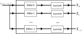
The main process of a typical PA algorithm is compressing the input sequence with a hash function randomly chosen from the universal hash family. The MMH-MH PA algorithm performs the compression twice with different universal hash families instead of once. The main steps of MMH-MH PA algorithm are indicated as Fig. 1, where is the length of input sequence. is the length of final key. The definition of multilinear modular hash and modular arithmetic hash are given as follow.
Definition of Multi-linear Modular Hashing
Let be a primer and let be an integer . Define a family multi-linear modular hashing of functions from to as follows:
| (1) |
where the function is defined for any , , ,
| (2) |
Definition of Modular Arithmetic Hashing
Let and be two strictly positive integers, . Define a family modular arithmetic hashing of functions from to as follows:
| (3) |
where the function is defined as follows:
| (4) |
Modular Arithmetic Hashing can be designed for PA algorithm itself, while it can not split the input and handle it separately. the output set of modular arithmetic hashing is variable length bit sequence. So it can be combined with MMH to design a new PA algorithm.
The specific process of the MMH-MH PA algorithm is given as Algorithm 1. In details, the prime number is suggested to be a Mersenne prime. The form of a Mersenne prime is . The length of input sequence is . is a special case, the data should be cast away and reload.
Because the process of MMH-MH PA is different from that of traditional PA algorithms, we have proven that the security of MMH-MH PA is similar with other PA algorithms in [12]. MMH-MH PA algorithm requires an additional condition to guarantee the security, that is the length of final key should be much less than , specifically ( is the information theory security parameter of QKD).
III Large-Scale and High Speed PA scheme on FPGA
A large-scale and high-speed PA scheme on the FPGA is designed based on MMH-MH PA algorithm in this section. It can be found that the major part of MMH-MH PA algorithm is the large-number multiplication according to Section 2. It is the core operation of both MMH function and MH function. Therefore, we designed a multiplication-reusable structure and its control unit for the scheme, and we introduced the calculation method of key parameters in this scheme. Afterwards, the design method of main units is illustrated. The most important unit is the large-number multiplication unit. It deeply determines the performance of the whole scheme. A 768Kb multiplication unit is designed based on number theoretic transform (NTT). In addition, it can optimize computation resource cost according to the real-time requirement by adjusting the radix of NTT. Then we designed a low-cost modular accumulation unit and a pipelined binary modular addition unit to improve overall performance.
III-A Architecture of large-scale PA scheme
The architecture of large-scale PA scheme is indicated as Fig. 2. The multiplication unit is reused in this architecture to reduce the resource cost. There are two streams of data flow in this scheme, and they represent the MMH function data stream and MH function data stream.

A matched control unit is designed to control computational process and data flow as indicated as Fig. 3. The MMH function calculation begins first when the multiplication unit is ready. Because MMH function needs times multiplication, the state will turn to ”MMH cnt” and a counter up one when one multiplication operation completes. The state will return to ”MMH” if and go to ”MH” if . ”MH” state will calculate MH function and output the final key, and the state will go back to initial state until the end of the output. The control unit will make data flow follow the blue arrow at the state ”MMH” and the red arrow at the state ”MH”.

III-B Key parameter calculation of large-scale PA scheme
The sub-block size and the sub-block number are the most critical parameter in this scheme. Because the input block size is the main optimization target, and are expected to be as larger as possible. is restricted by two conditions: 1. should be a primer; 2. should be less than the largest number supported by the large-number multiplication unit. The of multiplication unit in our implementation scheme is , so the sub-block size can be chosen as ( is the 32nd Mersenne prime). The largest number multiplication unit on FPGA as we know is the module in [15], and its . Therefore, the largest can be ( is the 33rd Mersenne prime). The sub-block number is restricted by the compression ratio of PA (The calculation method of can be referred in [12]), and should be larger than . The compression ratio is affected by the specific QKD system and transmission distance, so the specific value of will be discussed in next section.
Then we elaborate the design of three main modules of this scheme: 1. the large-number multiplication unit; 2. the low-cost modular accumulation unit 3. the pipelined binary modular addition unit.
III-C Design of large-number multiplication unit
The large number multiplication unit is the most essential and complex unit in this scheme. The size of this large number multiplication unit is bits. It is implemented based on number theoretical transform (NTT) algorithm. The large number multiplication algorithm () can be summarized as follow:
1) Break the large numbers and into a sequence of words and using base : and .
2) Compute the dot product of NTT results and : = .
3) Compute the inverse NTT (INTT) : .
4) Resolve the carries: let , and .
The base and the sequence size , so the size of this large number multiplication is . NTT and INTT are the main parts in this algorithm, and a 65536-point NTT and 65536-point INTT are required. An N-point NTT is defined as:
And an N-point INTT is defined as:
To simplify the modulo operation, is chosen as a special primer, which is . One data point in NTT is represented as a 64-bits digit. So the largest data point is , which is a 128-bits digit and represented as . It can be rewrite as,
The computation complexity of directly computing NTT is too excessive, so the butterfly algorithm is required to reduce it. The radix is an important parameter of butterfly algorithm. Larger radix will decrease the run time of algorithm and cost more computational resource. The radix- butterfly algorithm will be introduced next.
III-C1 Radix- butterfly algorithm
We take 16-point NTT as an example to demonstrate the difference between radix-2, radix-4, radix-16 butterfly algorithm. The computation of radix-16 is indicated as follow,
.
Obviously, the radix-16 algorithm only needs to run once to complete the 16-point NTT. The computation of radix-4 is indicated as follow,
.
The 16-point NTT can be divided into twice radix-4 calculation, the specific process is shown below,
,where and . In the same way, the 16-point NTT can be divided into quartic radix-2 calculation.
It is worth noting that the rotation factor can be the power of 2 when , such as . Then the multiplication can be replaced by shifting. A radix-r calculation structure can be indicated as Fig. 4. It can be found that the unit with larger radix- costs more computation resource.
To evaluate the real-time of scheme, we choose the best real-time selection, radix-16, in this scheme.
III-C2 structure of large-number multiplication unit
The structure of large-number multiplication unit is indicated as Fig. 5. The NTT processor used a radix-16 unit and matched memory to complete a -point NTT/INTT calculation. The calculation requires four stage to complete. The memory unit is divided into 16 banks to load 16-point data in one time. The data in memory should be stored by a well-designed address mapping table. Details of the well-designed address mapping table can be referred in [16].
The data is load into memory before the NTT calculation. In each stage of NTT, the data is access and transmit into the radix-16 unit. Then it is send to a 64-bit multiplication unit, and the multiplicand will be constant ’1’, rotation factor , INTT factor and the NTT results of NTT_B. The th primitive root of is 0x. After NTT and INTT calculation are completed, the data is load into the carry option module to guarantee each point of multiplication results is 24bits. More details of large-number multiplication unit can be found in [16].

III-D Design of low-cost modular accumulation unit
The low-cost modular accumulation unit is responsible for modular accumulate calculation in MMH function , where is the multiplication result of large-number multiplication unit and . The modular addition can be simplified as follow,
In this way, the modular calculation is replaced by addition and bit operation. It only needs full adders and bits memory. The structure is indicated as Fig. 6. In this structure, the input data just adds the data in accumulation result memory with period 756839 and clears memory when once MMH function completes.
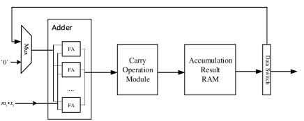
III-E Design of pipelined binary modular addition unit
The pipelined binary modular addition unit is designed to calculate the equation . The structure of pipelined binary modular addition unit is indicated as Fig. 7. has been prepared by multiplication unit and is the unit input. adder and carry operation module calculate . The binary modular and division is implemented by the data counter and switch module. The parameter is equal to and is equal to the length of secure key. Each frame of data is 24 bits, so the module begins to output data when the input data count is . The first frame of data outputs bits data. The rest of frames are 24bits each frame. The output ends when the data count is . This unit use data counter instead of calculation module implementing pipelining and low cost.

IV Implementation and Experiment
The proposed large-scale and high-speed (LSHS) PA scheme is implemented on the Xilinx ZYNQ ultrascale+ evaluate kit. This kit is based on a Zynq Ultrascale+ XCZU9EG-2FFVB1156 FPGA. The resource utilization is an important indicator to estimate the practicability of a FPGA-based PA scheme, and it is influenced by and in our scheme. The resource utilization of our scheme with and is indicated as Table. I.
| Resource | Scheme Used | Available1 | Utilization Rate |
| Luts | 156707 | 230400 | 68% |
| BRAMs | 198 | 408 | 48% |
| DSP Slices | 512 | 1728 | 30% |
-
1
Available: Zynq Ultrascale+ XCZU9EG-2FFVB1156 available
-
2
and
This scheme is evaluated in three aspects: 1. The input block size of the LSHS PA scheme is evaluated and the secure key rate improvement of a FPGA-based QKD system with LSHS PA scheme is demonstrated; 2. The throughput of the LSHS PA scheme on different block size is evaluated and compared with existing PA schemes; 3. The resource cost and core index of the LSHS PA scheme are compared with existing FPGA-based PA schemes.
IV-A The input block-size and secure key rate of the LSHS PA scheme
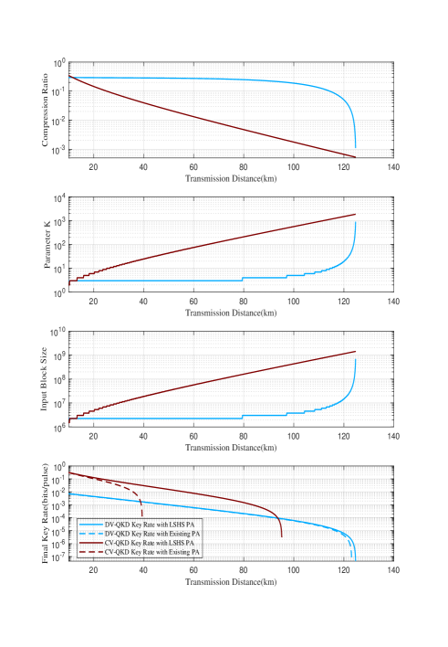
The input block size of the LSHS PA scheme is equal to . is a fixed value and is related to the maximum compression ratio of PA. Therefore, the input block size is related to the maximum compression ratio of PA. can be calculated on the basis of QKD system parameters. The compression ratio of a DV-QKD system can be calculated by . The compression ratio of a CV-QKD system can be calculated by . The main fluctuate factor of compression ratio is the channel error rate . The maximum compression ratio means the compression ratio when the channel error rate is minimum. The parameter is required to be smaller than to maximum the secure key rate.
The effect of the LSHS PA scheme on the input block size and secure key rate is evaluated by the simulation on a typical DV-QKD system [17] and a typical CV-QKD system [18]. The results demonstrate the parameter , the input block size and secure key rate as communication distance changes in Fig. 8. We computed the compression ratio of PA in two QKD systems at different transmission distances to confirm the parameter in the first subgraph. Here we assumed the input block size is infinite to compute the maximum compression ratio in the infinite input block size case. The parameter of the LSHS PA scheme was calculated according to the compression ratio of PA in the second subgraph. Then the input block size of the LSHS PA scheme at different transmission distances was confirmed with the parameter and the parameter in the third subgraph, where the input block size equals to . Finally, we simulated the final key rate of typical QKD systems with the LSHS PA scheme at different transmission distances in the last subgraph. The input block size of existing FPGA-based PA schemes is set to , because it is the largest input block size of existing FPGA-based PA schemes as we know. It can be found that the effect of the LSHS PA scheme is more significant in the CV-QKD system. This is because the finite size effect in the CV-QKD system is more serious than that in the DV-QKD system.
In conclusion, the simulation results indicate that the LSHS PA scheme can improve the input block size and the secure key rate of a QKD system. This improvement is more efficient in a CV-QKD system.
IV-B The throughput of the LSHS PA scheme
The throughput of PA means the maximum rate of the input key into a PA scheme. It is an important index of PA, which affects real-time of a QKD system. We experimented the throughput of the LSHS PA scheme at different input block sizes with a random simulated data source. Then, we compared the throughput between our scheme and existing schemes as indicated in Fig. 9 [9, 11, 17, 19].
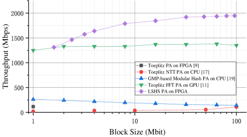
The comparison shows that our scheme improves the throughput by an order of magnitude than existing FPGA-based PA schemes, and our scheme reaches a equal throughput with the existing best throughput PA scheme – a GPU-based PA scheme. The throughput advantage of the LSHS PA scheme profits from two reasons: 1. the less computation of MMH-MH PA algorithm; 2. the three efficient units we design in section 3.
IV-C The resource cost and core index comparison of FPGA-based PA schemes
We compared the resource cost and core index between LSHS PA scheme and existing FPGA-based PA schemes. The resource cost of a FPGA-based PA scheme includes look up tables (LUTs), internal Random Access Memory (RAM), external RAM and DSP slices. The core index to be compared is throughput and input block size of a PA scheme. The comparison results are indicated as Table II.
The LSHS PA scheme costs the most LUT and Internal-RAM among existing PA schemes. The main cost of LSHS PA is the large-number multiplication unit. It costs nearly of LSHS PA scheme. The main reason of its high cost is that it chooses the radix of the unit as . This provides the best real-time and throughput, but also costs the most resource. If a large-number multiplication unit with is used in this scheme, we estimated that the throughput and the LUTs cost will be reduced to approximately eighth of their previous. The internal-RAM cost of the LSHS scheme is the most, because it uses the NTT algorithm for acceleration, and the NTT algorithm needs to store all the input data and rotation factors. Similarly, the scheme in [9] used the FFT algorithm for acceleration. The NTT algorithm has an advantage over FFT algorithm, that the data format of the NTT is the integer instead of the floating-point of the FFT. This advantage significantly reduces the memory cost of the LSHS scheme compared with the scheme in [9], and frees the LSHS PA scheme from dependence on the external-RAM.
| Yang et al. | Constantin et al. | Li et al. | LSHS PA | |
| LUTs | 15,604 | 26,571 | 37,203 | 156,707 |
| Internal-RAM | 100Kb | 0Kb | 5,652Kb | 11,232Kb |
| External-RAM | 0Kb | 1,095Kb | 128Mb | 0Kb |
| Throughput | 64Mbps | 41Mbps | 116Mbps | 1,400Mbps |
| Input Block Size | 1Mb | 1Mb | 1Mb | 1-1000Mb |
Although the LSHS PA scheme costs more resources, the LSHS PA scheme greatly improves the core index of FPGA-based PA scheme. Before the LSHS PA scheme, the throughput and input block size of the FPGA-based PA scheme is far below that of PA schemes based on other platforms. Therefore, although FPGA-based PA schemes have advantages of low power consumption and high integration level for QKD systems, they are not applied widely due to the low core index. The core index of the LSHS PA scheme has exceeded existing FPGA-based PA schemes by several orders of magnitude, and it has surpassed the best PA scheme in term of these core indexes.
V Conclusion
In this research, a large scale and high speed PA scheme based on FPGA is proposed to improve the core index (input block size and throughput) of a FPGA-based PA scheme. This scheme is designed based on the MMH-MH PA algorithm. We designed the architecture of the LSHS PA scheme to reuse as many computation unit as possible for the resource cost reduction. Then we focused on the design of three key units of this scheme in this paper. A 786432-bits large-number multiplication unit is designed based on the NTT algorithm. A low-cost modular accumulation unit is designed to compute accumulation with minimal memory. A pipelined binary modular addition is designed to compute the binary modular of arbitrarily length without memory. We implemented the proposed large-scale and high-speed PA scheme on the Xilinx ZYNQ ultrascale+ evaluate kit. We referenced the parameters of a typical DV-QKD system and a typical CV-QKD system to evaluate the input block size, the throughput and the influence on the final key rate of the LSHS PA scheme. We compared these results with existing PA schemes on FPGA and other platforms. The results indicate that the LSHS PA scheme has improved the throughput by an order of magnitude, and it can improve the input block size by several magnitudes compared with existing FPGA-based PA schemes. The input block size improvement is more obvious in a CV-QKD system and a long transmission distance QKD system. The above results indicates that the LSHS PA scheme can significantly improve the final key rate of a FPGA-based QKD system. It is worth noting that the core index of the LSHS PA scheme has exceed the existing best PA scheme of all platforms. Adding the consideration with the power consumption and integration level advantages of the FPGA-based PA schemes, the LSHS PA scheme is a highly competitive solution for the QKD systems.
References
- [1] G. Bennett, Charles and Brassard, “Quantum cryptography: Public key distribution and coin tossing,” Theoretical Computer Science - TCS, vol. 560, pp. 175–179, 1984.
- [2] H. Mao, Q. Li, Q. Han, and H. Guo, “High Throughput and Low Cost LDPC Reconciliation for Quantum Key Distribution,” Quantum Information Processing, vol. 2, 2019. [Online]. Available: http://arxiv.org/abs/1903.10107
- [3] H. F. Zhang, J. Wang, K. Cui, C. L. Luo, S. Z. Lin, L. Zhou, H. Liang, T. Y. Chen, K. Chen, and J. W. Pan, “A real-time QKD system based on FPGA,” Journal of Lightwave Technology, vol. 30, no. 20, pp. 3226–3234, 2012.
- [4] J. Constantin, R. Houlmann, N. Preyss, N. Walenta, H. Zbinden, P. Junod, and A. Burg, “An FPGA-Based 4 Mbps Secret Key Distillation Engine for Quantum Key Distribution Systems,” Journal of Signal Processing Systems, vol. 86, no. 1, pp. 1–15, 2017. [Online]. Available: http://dx.doi.org/10.1007/s11265-015-1086-1
- [5] P. Sibson, C. Erven, M. Godfrey, S. Miki, T. Yamashita, M. Fujiwara, M. Sasaki, H. Terai, M. G. Tanner, C. M. Natarajan, R. H. Hadfield, J. L. O’Brien, and M. G. Thompson, “Chip-based quantum key distribution,” Nature Communications, vol. 8, no. May 2016, 2017.
- [6] C. H. Bennett, G. Brassard, C. Crkpeau, U. M. Maurer, and S. Member, “Generalized privacy amplification,” Information Theory, IEEE Transactions on, vol. 41, no. 6, pp. 1915–1923, 1995. [Online]. Available: http://ieeexplore.ieee.org/xpls/abs_all.jsp?arnumber=476316
- [7] F. Furrer, T. Franz, M. Berta, A. Leverrier, V. B. Scholz, M. Tomamichel, and R. F. Werner, “Continuous variable quantum key distribution: Finite-key analysis of composable security against coherent attacks,” Physical Review Letters, vol. 109, no. 10, pp. 1–5, 2012.
- [8] M. Tomamichel, C. C. W. Lim, N. Gisin, and R. Renner, “Tight finite-key analysis for quantum cryptography,” Nature Communications, vol. 3, p. 634, 2012.
- [9] Q. Li, B. Z. Yan, H. K. Mao, X. F. Xue, Q. Han, and H. Guo, “High-Speed and Adaptive FPGA-Based Privacy Amplification in Quantum Key Distribution,” IEEE Access, vol. 7, pp. 21 482–21 490, 2019.
- [10] B. Y. Tang, B. Liu, Y. P. Zhai, C. Q. Wu, and W. R. Yu, “High-speed and Large-scale Privacy Amplification Scheme for Quantum Key Distribution,” Scientific Reports, vol. 9, no. 1, pp. 1–8, 2019. [Online]. Available: http://dx.doi.org/10.1038/s41598-019-50290-1
- [11] X. Wang, Y. Zhang, S. Yu, and H. Guo, “High-speed implementation of length-compatible privacy amplification in continuous-variable quantum key distribution,” IEEE Photonics Journal, vol. 10, no. 3, pp. 1–9, 2018.
- [12] Y. Bingze, L. Qiong, M. Haokun, and C. Nan, “An efficient hybrid hash based privacy amplification algorithm for quantum key distribution,” 2021. [Online]. Available: http://arxiv.org/abs/2105.13678
- [13] J. L. J. Carter and M. M. N. M. Wegman, “Classes of Hash Functions,” Journal of computer and system sciences, vol. 18, pp. 143–154, 1979. [Online]. Available: http://www.sciencedirect.com/science/article/pii/0022000079900448
- [14] S. Halevi and H. Krawczyk, “MMH: Software message authentication in the Gbit/second rates,” Lecture Notes in Computer Science (including subseries Lecture Notes in Artificial Intelligence and Lecture Notes in Bioinformatics), vol. 1267, pp. 172–189, 1997.
- [15] J. H. Ye and M. D. Shieh, “Low-Complexity VLSI Design of Large Integer Multipliers for Fully Homomorphic Encryption,” IEEE Transactions on Very Large Scale Integration (VLSI) Systems, vol. 26, no. 9, pp. 1727–1736, 2018.
- [16] W. Wang, X. Huang, N. Emmart, and C. Weems, “VLSI design of a large-number multiplier for fully homomorphic encryption,” IEEE Transactions on Very Large Scale Integration (VLSI) Systems, vol. 22, no. 9, pp. 1879–1887, 2014.
- [17] Z. L. Yuan, A. Plews, R. Takahashi, K. Doi, W. Tam, A. W. Sharpe, A. R. Dixon, E. Lavelle, J. F. Dynes, A. Murakami, M. Kujiraoka, M. Lucamarini, Y. Tanizawa, H. Sato, and A. J. Shields, “10 Mb / s quantum key distribution,” Journal of Lightwave Technologyechnology, vol. 8724, no. c, pp. 1–7, 2018.
- [18] Y. Zhang, Z. Li, Z. Chen, C. Weedbrook, Y. Zhao, X. Wang, Y. Huang, C. Xu, X. Zhang, Z. Wang, M. Li, X. Zhang, Z. Zheng, B. Chu, X. Gao, N. Meng, W. Cai, Z. Wang, G. Wang, S. Yu, and H. Guo, “Continuous-variable QKD over 50 km commercial fiber,” Quantum Science and Technology, vol. 4, no. 3, pp. 0–12, 2019.
- [19] B. Yan, Q. Li, H. Mao, and X. Xue, “High-Speed Privacy Amplification Scheme Using GMP in Quantum Key Distribution,” IEEE Photonics Journal, vol. 12, no. 3, pp. 1–13, 2020.