Electrostatic field-driven supercurrent suppression in ionic-gated metallic Josephson nanotransistors
Abstract
Recent experiments have shown the possibility to tune the electron transport properties of metallic nanosized superconductors through a gate voltage. These results renewed the longstanding debate on the interaction between intense electrostatic fields and superconductivity. Indeed, different works suggested competing mechanisms as the cause of the effect: unconventional electric field-effect or quasiparticle injection. By realizing ionic-gated Josephson field-effect nanotransistors (IJoFETs), we provide the conclusive evidence of electrostatic field-driven control of the supercurrent in metallic nanosized superconductors. Our Nb IJoFETs show bipolar giant suppression of the superconducting critical current up to with negligible variation of both the critical temperature and the normal-state resistance, in a setup where both overheating and charge injection are impossible. The microscopic explanation of these results calls upon a novel theory able to describe the non-trivial interaction of static electric fields with conventional superconductivity.
Since the discovery of superconductivity, the impact of electrostatic fields on metallic superconductors is an open issue. Seminal experiments showed modulations of the superconducting critical temperature () and normal-state resistance () in tin and indium films [1, 2] by conventional charge accumulation/depletion. Recently, gate voltage () induced bipolar full supercurrent suppression was demonstrated via conventional solid gating in several metallic superconducting nanostructures, such as wires [3], constriction Josephson junctions [4], and proximitized normal metals [5]. Similar results were obtained also on suspended [6] and epitaxial [7] superconducting metal layers grown on semiconductor nanowires. Differently from charge accumulation/depletion, this gating effect seems to influence as well the phase of the Cooper pairs condensate [8, 9, 10] without apparent impact on and [11], thereby suggesting a non-trivial interaction between electrostatic fields and superconductivity. Yet, subsequent works attempted to explain the critical current () suppression in terms of overheating due to quasiparticle injection into the transistor channel [12, 13], cold electron field-emission either from the gate electrode or the channel [14, 15] and non-equilibrium phonon-mediated interaction [16], although with clear inability to reconcile together all previous experimental evidences. Moreover, quasiparticle overheating by itself is not able to account for the enhancement of the critical current observed in NbN nanobridges subject to conventional gating [17]. Therefore, the microscopic origin of this phenomenon is still unknown and under a strong scientific debate. Beyond the profound relevance for fundamental science, electric field control of supercurrents in metallic superconductors would enable the implementation of a groundbreaking low-dissipation and energy-efficient superconducting electronics.
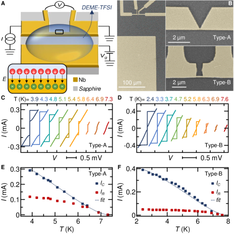
Here, we provide the unequivocal demonstration of electrostatic field-induced giant suppression in metallic superconductors by exploiting ionic-gated Nb Josephson field-effect nanotransistors (IJoFETs, Fig. 1A). By applying across an electrolyte (DEME-TFSI), ionic gating enables the generation of intense electrostatic fields () by forming the so-called electric double layer (EDL) at the sample surface (inset), in the absence of electron leakage currents. This technique is routinely used to tune the transport properties of micro-scale metals [18] and metallic superconductors [19, 20] (i.e., and ) by charge accumulation/depletion, as it occurs in conventional semiconductor devices. Instead, we downsized to the nano-scale the channel of Nb IJoFETs (Fig. 1B) to study the impact of on the supercurrent flow, i.e., by measuring their versus characteristics. In particular, we realized different geometries by sputtering a niobium film on a sapphire substrate: Type-A devices are Josephson nanoconstrictions realized by a bottom-up approach, while Type-B samples are nanowires fabricated by a top-down method (details are provided in the supplementary materials). A common feature to both structures is the large distance (m) existing between the gate electrode and the IJoFET channel, which prevents any conventional electron leakage current stemming from the application of the polarization voltage to the electrolyte ( V for DEME-TFSI). Type-A and Type-B nanotransistors show the typical hysteretic current-voltage () characteristic of diffusive superconducting weak-links [21] (Fig. 1, C and D), where the transition current from the normal to the superconducting state is known as retrapping current (). As expected, and decrease monotonically with bath temperature () until their full suppression at (Fig. 1, E and F). In particular, the devices show K and K for Type-A and Type-B structure, respectively. In addition, follows the Bardeen theoretical curve [22] (dashed lines), where A and A are the zero-temperature critical currents obtained from the fit of Type-A and Type-B devices, respectively.
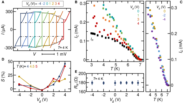
We now focus on the electrostatic control of the supercurrent in a Type-A IJoFET consisting of a Josephson nanoconstriction (Fig. 1B). To this end, we measured the characteristics as a function of bath temperature for different values of . Since the ions in the electrolyte are frozen and immobile at cryogenic temperatures, we applied at room temperature before cooling down the devices (details are provided in the supplementary materials). Figure 2A shows the characteristics recorded at K for different values of . The critical current decreases with the amplitude of the gate voltage for both positive and negative polarities of (dotted lines), while turns out to be unaffected by gating effect (dash-dotted lines). We emphasize that at V we also disconnected the gate voltage source at cryogenic temperatures (i.e., when the ions are frozen in a fixed configuration) yielding no variation on the suppression of , thereby further excluding any relation between the critical current suppression and the leakage currents. The general behavior of as a function of is shown in Fig. 2B for selected positive values of . The critical current is strongly suppressed by at low temperature, while all the curves collapse into the zero-gate trace for . This behavior resembles the temperature dependence of the critical current measured in conventionally-gated Ti nano constrictions [11]. Furthermore, in full agreement with previous experiments on Nb Josephson nano-bridges [23], this unconventional gating has no effect on the critical temperature of the nanosized superconductor. We stress that is also suppressed for negative values of the gate voltage (Fig. 2C). The bipolarity of gating effect can be quantified via the suppression parameter, defined as . The parameter increases with the magnitude of for both polarities, reaching its maximum of at V and K (Fig. 2D). Remarkably, the normal-state resistance of Type-A IJoFETs is unaffected by the gating (Fig. 2E). These features suggest that charge accumulation/depletion is not driving the supercurrent suppression in our devices.
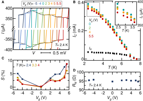
To examine whether this unconventional gating effect is general or related to a specific sample geometry, we performed similar experiments on Type-B IJoFETs, where the superconducting channel consists of a long Nb nanowire (Fig. 1B). Notably, the overall qualitative behavior of this structure is analogous to Type-A sample. Indeed, the characteristics of a typical Type-B IJoFET recorded at K show bipolar suppression with the gate voltage (Fig. 3A). At a given value of , the supercurrent is strongly reduced at low temperatures, whereas it approaches the zero-gate value by increasing the temperature (Fig. 3B). Furthermore, the superconducting critical temperature and the retrapping current are -independent. As a consequence of the versus characteristics, the suppression parameter decreases with temperature for both polarities of gate voltage (Fig. 3C). Similarly to Type-A IJoFET (Fig. 2D), gating effect is more pronounced for positive values of gate voltage ( at V), due to the higher polarization efficiency of the employed electrolyte (DEME-TFSI) [24]. Finally, the normal-state resistance of the nanotransistor channel is not affected by gating, since does not show any clear trend with (Fig. 3D).
The phenomenology shown by Type-A and Type-B IJoFETs fully resembles the effect of conventional solid gating observed so far on nanosized superconducting systems [3, 4, 5, 6, 7, 8, 9, 11, 23]. The absence of full supercurrent suppression in the IJoFETs might be ascribed to the profile of the electric field generated by ionic gating. Indeed, lateral solid gates tend to produce localized and strongly anisotropic electric fields [5, 6], while electrolytes tend to generate rather isotropic electric field profiles on the nanotransistors channel surface. Since ionic gating avoids any leakage current, we conclude that the observed supercurrent suppression is exclusively driven by the electrostatic field therefore ruling out any quasiparticle injection-related mechanism at the origin of the effect [12, 13, 14, 15, 16]. Moreover, the observed bipolarity together with the invariance of and also exclude significant modulations of the superconductor chemical potential due to charge accumulation/depletion which, differently, were reported in ionic-gated micro-scale metals in the normal [18] and superconducting [19, 20] state. This difference might stem from the nanoscale channel of our IJoFETs as compared to the micro-scale one of other works on Nb thin films, or from the superconducting film thickness [19]. As a consequence of the chemical potential steadiness, this unconventional field-effect seems not to act directly on the amplitude of the pairing potential but suggests a non-trivial interaction with the superconducting macroscopic phase [8, 9]. Since the microscopic nature of such interaction is still almost entirely unknown, further experimental and theoretical investigations are required to shed light on this gating effect.
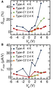
We wish to finally comment the performance of our Nb IJoFETs from the application point of view. To this end, it is interesting to compare the maximum suppression parameter obtained in various IJoFETs. Figure 4A shows for different IJoFET geometries. In particular, samples discussed so far are also compared with an additional set of Type-C devices, that are Josephson nano-constrictions realized by a bottom-up approach on top of a silicon dioxide substrate (details are provided in the supplementary materials). The suppression parameter seems to be generally larger for devices fabricated with a bottom-up approach (Type-A and Type-C), since possible tiny resist residues originating from the etching mask might increase the distance between the charge planes forming the EDL at the surface of the superconducting channel, thereby yielding a reduced electric field. Moreover, in light of possible applications, it is worth to discuss the transconductance of the IJoFETs, a key figure of merit for field-effect transistors. For the IJoFETs, it can be defined as , where . Figure 4B shows the maximum value of versus deduced for four different IJoFETs. Notably, for all our ionic-gated devices, (which obtains values as high as A/V) is comparable to the transconductance achieved so far in conventional superconducting [25], Josephson [26], and all-metallic field-effect nanotransistors [4].
In conclusion, our work provides the clear and unambiguous proof of the non-conventional and disruptive impact of intense electrostatic fields on the supercurrent flow in nano-sized metallic superconductors. The use of ionic gating rules out both quasiparticle overheating and any other charge injection-based mechanism at the origin of the effect. Moreover, the bipolar supercurrent suppression observed in IJOFETs of different geometries, along with the absence of critical temperature and normal-state resistance variations, exclude conventional charge accumulation/depletion. Therefore, our results advise for further theoretical and experimental investigations to unveil the microscopic genesis of field-effect in metallic superconductors. From the technological side, our IJoFETs might be at the basis of innovative combined ionic-solid-gating devices suitable for a number of different applications in leading-edge superconducting electronics, quantum computing, and sensing.
References
- [1] R. Glover, M. Sherrill, Changes in superconducting critical temperature produced by electrostatic charging, Phys. Rev. Lett. 5, 248 (1960).
- [2] H. L. Stadler, Changing Properties of Metals by Ferroelectric Polarization Charging, Phys. Rev. Lett. 14, 979 (1965).
- [3] G. De Simoni, F. Paolucci, P. Solinas, E. Strambini, F. Giazotto, Metallic supercurrent field-effect transistor, Nat. Nanotech. 13, 802 (2018).
- [4] F. Paolucci, G. De Simoni, P. Solinas, E. Strambini, F. Giazotto, Ultra-Efficient Superconducting Dayem Bridge Field-Effect Transistor, Nano Lett. 18, 4195 (2018).
- [5] G. De Simoni, F. Paolucci, C. Puglia, F. Giazotto, Josephson Field-Effect Transistors Based on All-Metallic Al/Cu/Al Proximity Nanojunctions, ACS Nano 13, 7871 (2019).
- [6] M. Rocci, G. De Simoni, C. Puglia, D. Degli Esposti, E.Strambini, V. Zannier, L. Sorba, F. Giazotto, Gate-Controlled Suspended Titanium Nanobridge Supercurrent Transistor, ACS Nano 14, 12621 (2020).
- [7] T. Elalaily, O. Kürtössy, Z. Scherübl, M. Berke, G. Fülöp, I. E. Lukács, T. Kanne, J. Nygård, K. Watanabe, T. Taniguchi, P. Makk, S. Csonka, Gate-controlled supercurrent in an epitaxial Al/InAs nanowires, arXiv e-prints 2106.06619 (2021).
- [8] F. Paolucci, F. Vischi, G. De Simoni, C. Guarcello, P. Solinas, F. Giazotto, Field-Effect Controllable Metallic Josephson Interferometer, Nano Lett. 19, 6263 (2019).
- [9] C. Puglia, G. De Simoni, F. Giazotto, Electrostatic Control of Phase Slips in Ti Josephson Nanotransistors, Phys. Rev. Appl. 13, 054026 (2020).
- [10] G. De Simoni, S. Battisti, N. Ligato, M. T. Mercaldo, M. Cuoco, F. Giazotto, Gate-control of the current-flux relation of a Josephson quantum interferometer based on proximitized metallic nanojuntions, arXiv e-prints 2106.03572 (2021).
- [11] F. Paolucci, G. De Simoni, P. Solinas, E. Strambini, N. Ligato, P. Virtanen, A. Braggio, F. Giazotto, Magnetotransport Experiments on Fully Metallic Superconducting Dayem-Bridge Field-Effect Transistors, Phys. Rev. Appl. 11, 024061 (2019).
- [12] M. F. Ritter, A. Fuhrer, D. Z. Haxell, S. Hart, P. Gumann, H. Riel, F. Nichele, A superconducting switch actuated by injection of high-energy electrons, Nat. Commun. 12, 1266 (2021).
- [13] G. Catto, W. Liu, S. Kundu, V. Lahtinen, M. Möttönen, Microwave response of a metallic superconductor subject to a high-voltage gate electrode, arXiv e-prints 2105.08322 (2021).
- [14] I. Golokolenov, A. Guthrie, S. Kafanov, Y. A. Pashkin, V. Tsepelin, On the origin of the controversial electrostatic field effect in superconductors, Nat. Commun. 12, 2747 (2021).
- [15] L. D. Alegria, C. G. L. Bøttcher, A. K. Saydjari, A. T. Pierce, S. H. Lee, S. P. Harvey, U. Vool, A. Yacoby, High-energy quasiparticle injection into mesoscopic superconductors, Nat. Nanotech. 16, 404 (2021).
- [16] M. F. Ritter, N. Crescini, D. Z. Haxell, M. Hinderling, H. Riel, C. Bruder, A. Fuhrer, F. Nichele, On the Role of Out-of-Equilibrium Phonons in Gated Superconducting Switches, arXiv e-prints 2106.01816 (2021).
- [17] M. Rocci, D. Suri, A. Kamra, G. Viela, Y. Takamura, N. M. Nemes, J. L. Martinez, M Garcia Hernandez, J. S. Moodera, Large Enhancement of Critical Current in Superconducting Devices by Gate Voltage, Nano Lett. 21, 216 (2021).
- [18] D. Daghero, F. Paolucci, A. Sola, M. Tortello, G. A. Ummarino, M. Agosto, R. S. Gonnelli, J. R. Nair, C. Gerbaldi, Large conductance modulation of gold thin films by huge charge injection via electrochemical gating, Phys. Rev. Lett. 108, 066807 (2012).
- [19] D. Choi, R. Pradheesh, H. Kim, H. Im, Y. Chong, D.-H. Chae, Electrical modulation of superconducting critical temperature in liquid-gated thin niobium films, Appl. Phys. Lett. 105, 012601 (2014).
- [20] E. Piatti, Ionic gating in metallic superconductors: A brief review, Nano Ex. 2, 024003 (2021).
- [21] H. Courtois, M. Meschke, J. T. Peltonen, J. P. Pekola, Origin of Hysteresis in a Proximity Josephson Junction, Phys. Rev. Lett. 101, 067002 (2008).
- [22] J. Bardeen, Critical Fields and Currents in Superconductors, Rev. Mod. Phys. 34, 667 (1962).
- [23] G. De Simoni, C. Puglia, F. Giazotto, Niobium Dayem nano-bridge Josephson gate-controlled transistors, Appl. Phys. Lett. 116, 242601 (2020).
- [24] T. Sato, G, Masuda, K. Takagi, Electrochemical properties of novel ionic liquids for electric double layer capacitor applications, Electrochimica Acta 49, 3603 (2004).
- [25] T. Nishino, M. Hatano, H. Hasegawa, F. Murai, T. Kure, A. Hiraiwa, K. Yagi, U. Kawabe, 0.1- mu m gate-length superconducting FET, IEEE Electron Device Lett. 10, 61 (1989).
- [26] T. D. Clark, R. J. Prance, A. D. C. Grassie, Feasibility of hybrid Josephson field effect transistors, J. Appl. Phys. 51, 2736 (1980).
- [27] A. R. Jani, N. E. Brener, J. Callaway Band structure and related properties of bcc niobium, Phys. Rev. B 38, 9425 (1988).
- [28] J. Bardeen, Critical Fields and Currents in Superconductors, Rev. Mod. Phys. 34, 667 (1962).
- [29] H. Yuan, H. Shimotani, J. Ye, S. Yoon, H. Aliah, A. Tsukazaki, M. Kawasaki, Y. Iwasa, Electrostatic and Electrochemical Nature of Liquid-Gated Electric-Double-Layer Transistors Based on Oxide Semiconductors, J. Am. Chem. Soc. 132, 18402 (2010).
Acknowledgements
The authors acknowledge the European Research Council under Grant Agreement No. 899315 (TERASEC), and the EU’s Horizon 2020 research and innovation program under Grant Agreement No. 800923 (SUPERTED) and No. 964398 (SUPERGATE) for partial financial support.
Author contributions
F.P., G.D.S., L.B. and C.P. fabricated the samples. F.P., F.C. and L.B. performed the experiments with inputs from G.D.S., E.S, S.R. and F.G.. F.P. and F.C. analysed the experimental data with inputs from F.G.. F.P. and F.G. wrote the manuscript with inputs from all authors. F.G. supervised the experiment. All authors discussed the results and their implications equally at all stages.
Competing Interests
The authors declare no competing financial interests.
Supplementary Material for Electrostatic field-driven supercurrent suppression in ionic-gated metallic Josephson nanotransistors
Fabrication protocols
Type-A IJoFETs were fabricated by bottom-up approach on a sapphire substrate. A single-step electron-beam lithography (EBL) was realized to pattern a polymethyl-methacrylate (PMMA, thickness nm) evaporation mask. To avoid charging of the insulating substrate, a conductive polymer (Elttra 92) was spin-coated on the PMMA layer before the EBL. After the development of the resist mask, a 5-nm-thick Ti adhesion layer was dc-sputtered before the superconducting Nb film of thickness nm. After the lift-off procedure, the resulting nanotransitor channel is a nanoconstriction Josephson junction of length nm and width nm. The gate counter electrode is distant m from the transistor channel. After wire-bonding the device on a suited chip carrier, a drop of diethylmethyl(2-methoxyethyl)ammonium bis(trifluoromethylsulfonyl)imide (DEME-TFSI) was placed on the device.
Type-B IJoFETs were fabricated by top-down approach on a sapphire substrate. A 5-nm-thick Ti adhesion layer was dc-sputtered before the superconducting Nb film of thickness nm. A single-step EBL was realized to pattern the PMMA (thickness nm) etching mask. After the development, a step of inductively coupled plasma reactive ion etching [ICP-RIE, BCl3 (8 sccm)/Cl2 (6 sccm)/Ar (10 sccm)] etches the Nb film defining the device. The resulting nanotransitor channel is a nanowire of length m and width nm. The gate counter electrode is distant m from the transistor channel. After wire-bonding the device on a suited chip carrier, a drop of DEME-TFSI was placed on the device.
Type-C IJoFETs were fabricated by bottom-up approach on a silicon substrate covered by 300 nm of thermally grown dry silicon dioxide. A single-step EBL was realized to pattern a polymethyl-methacrylate (PMMA, thickness nm) evaporation mask. After the development of the resist mask, a 5-nm-thick Ti adhesion layer was dc-sputtered before the superconducting Nb film of thickness nm. The resulting nanotransitor channel is a nanoconstriction Josephson junction of length nm and width nm. The gate counter electrode is distant m from the transistor channel. After wire-bonding the device on a suited chip carrier, a drop of DEME-TFSI was placed on the device.
Measurement set-up
The measurements were performed from room temperature down to 2.4 K in a dry cryostat (OptistatDry, Oxford Instruments) equipped with RC-fiters of resistance k. The gate voltage was applied by means of a semiconductor characterization system (Keithley 4200). The current versus voltage characteristics of the IJoFETs were obtained by applying a biasing current through a low noise source (GS200, Yokogawa) and measuring the voltage drop by a room-temperature battery-powered differential preamplifier (Model 1211, DL Instruments). Alternatively, the device characterization was performed by a 750-KHz bandwidth input/output analog-to-digital/digital-to-analog converter (ADC/DAC, National Instruments) board for the generation of the bias current and the acquisition of the voltage drop signal arising from a room-temperature battery-powered differential preamplifier (Model 1211, DL Instruments). In both cases, we performed several repetitions of the IV characteristics (up to 50 depending on the device).
Polarization of the electrolyte
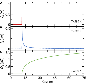
Figure S1 shows a typical charging characteristic of our IJoFETS recorded at room temperature ( K) before cooling down the devices to cryogenic temperatures for the electronic transport experiments. When a gate voltage is applied (panel A, V), a peak in the ionic current appears (panel B, ) due to the formation of the electric double layers (EDLs) at the interfaces of the electrolyte with the nanotransistor channel and the gate counterelectrode. On the one hand, shows a fast decay with time. On the other hand, an ionic current several orders of magnitude lower than the peak value is always present, since a charge flow is necessary into the electrolyte to maintain the gradient of ionic concentration [29]. The ionic charge displaced in the electrolyte is given by
| (S1) |
where is the time. Figure S1C shows the typical time dependence of : an exponential charging with time during the EDLs formation and, later, a square dependence with time () due to electrochemical effects in the electrolyte bulk.
Electronic transport in Type-C IJoFETs
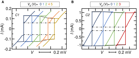
We present the electrostatic control of the supercurrent in Type-C IJoFETs consisting of a Josephson nanoconstriction fabricated with top-down approach on a silicon substrate covered with 300 nm of thermally grown silicon dioxide. Since the electrolyte can be polarized only at high temperature, we applied the gate voltage at room temperature and, then, we cooled down the devices to cryogenic temperatures to investigate the behavior of the supercurrent with temperature while a strong electrostatic field is present. To this end, we recorded the characteristics at different values of as a function of temperature. Figure S2 shows the characteristics recorded at K for different values of gate voltage of devices C1 (panel A) and C2 (panel B), respectively. The critical current decreases with the amplitude of the gate voltage (dotted black lines), while turns out to be almost unaffected by gating effect (dashed-dotted black lines). In particular, decreases of at V for sample C1, while it id suppressed of about at V for sample C2.
Devices parameters
Based on the device structure and transport properties, we can estimate several parameters of the superconducting Nb film, such as the normal-stare resistance (), the critical temperature (), the zero-temperature Bardeen-Cooper-Schrieffer (BCS) energy gap (), and the zero-temperature critical current ().
The normal-state resistance is obtained by a linear fit of the current versus voltage characteristics in the dissipative state. The error bars arise from the averages between the values of obtained from the fit procedure on the different repetitions.
The zero-temperature BCS superconducting energy gap can be calculated from
| (S2) |
where is the Boltzmann constant and is the superconducting critical temperature.
The phenomenological Bardeen model for the temperature dependence of the superconducting critical current reads [28]
| (S3) |
where is the zero-temperature critical current.
The basic parameters deduced for every device are resumed in the following table.
| DEVICES PARAMETERS | |||
|---|---|---|---|
| Sample | [K] | [] | [eV] |
| Type-A | 7.3 | 180 | 1.11 |
| Type-B | 7.6 | 94.6 | 1.15 |
| Type-C1 | 5.4 | 18 | 0.82 |
| Type-C2 | 6.4 | 28.8 | 0.97 |