Atomistic spin textures on-demand in the van der Waals layered magnet CrSBr
Abstract
Controlling magnetism in low dimensional materials is essential for designing devices that have feature sizes comparable to several critical length scales that exploit functional spin textures, allowing the realization of low-power spintronic and magneto-electric hardware. [1] Unlike conventional covalently-bonded bulk materials, van der Waals (vdW)-bonded layered magnets [2, 3, 4] offer exceptional degrees of freedom for engineering spin textures. [5] However, their structural instability has hindered microscopic studies and manipulations. Here, we demonstrate nanoscale structural control in the layered magnet CrSBr creating novel spin textures down to the atomic scale. We show that it is possible to drive a local structural phase transformation using an electron beam that locally exchanges the bondings in different directions, effectively creating regions that have vertical vdW layers embedded within the horizontally vdW bonded exfoliated flakes. We calculate that the newly formed 2D structure is ferromagnetically ordered in-plane with an energy gap in the visible spectrum, and weak antiferromagnetism between the planes. Our study lays the groundwork for designing and studying novel spin textures and related quantum magnetic phases down to single-atom sensitivity, potentially to create on-demand spin Hamiltonians probing fundamental concepts in physics, [6, 7, 8, 9, 10] and for realizing high-performance spintronic, magneto-electric and topological devices with nanometer feature sizes. [11, 12]
The observation of long-range magnetic order in the van der Waals (vdW) magnets CrI3 [2], Cr2Ge2Te6 [3] and Fe3GeTe2 [4] has expanded material platforms for the study of low-dimensional magnetism. Such pioneering work has strong relevance for exploring fundamental questions in physics, including probing the Mermin-Wagner-Hohenberg theorem [9, 10] and realizing spintronic and magneto-electric devices [13, 14, 15, 16, 17, 18] that allow voltage-controlled magnetic and spin related properties. [4, 19, 20, 21] Microscopically, such properties are governed by local coupling between spins that are strictly connected to the underlying crystal lattice. [22, 23] Thus, creating new degrees of freedom requires tailoring local structural properties. [24] Beyond the influence of the periodic crystal structure on the local magnetic coupling, chemical and structural defects as well as interfaces between domains, twins or confined geometries have been shown to produce exotic low-dimensional spin textures with novel chiralities, [25, 26, 27, 28] but controlled engineering of such defect topologies has proven to be challenging for further advancement in this field. [29]
In contrast to 3D materials, layered magnets offer superior design opportunities for engineering both periodic and non-periodic structures, and therefore spin textures, down to a single atomic level. Intrinsic (naturally occurring) spin textures below the critical temperature are made up of domain walls formed due to thermodynamically driven spin neutrality, while twin/grain boundaries and multicrystals are structural modulations that generally form naturally in structures to increase the entropy of the system. A hitherto overlooked aspect of vdW magnets is their potential for atomic scale structural modifications using electron or ion beam irradiation for the controlled creation of zero- to high dimensional defect topologies that range from single vacancies to locally induced crystal phase changes. [30] Of particular interest is the exploration of interfaces and their proximity effects that provide a playground for studying local chirality, [25] magnetic anisotropy and spin canting on ultra-short length scales. Deterministic engineering of previously studied vdW magnets has remained elusive due to their poor structural stability, since full encapsulation and protection in a glove box environment and sophisticated fabrication methods are required. [4, 2]
In this report, we demonstrate a versatile approach to engineer the structural landscape and the related spin textures in layered vdW magnets with single-atom precision. We conduct our study on the recently rediscovered vdW layered magnet CrSBr [31, 32, 33, 34] that constitutes an ideal candidate due to its known amenability for intrinsic structural changes [32] and its highly promising electronic, optical and magnetic properties. [31, 32, 33, 34, 35, 36, 37] CrSBr is an air-stable ferromagnetic (FM) insulator in the monolayer limit with a direct band gap of [35, 34, 33] hosting tightly bound magneto-excitons. [37] The magnetic easy axis is in-plane with an antiferromagnetic (AFM) interlayer coupling in the bulk with a Néel temperature of [32, 36] and a recently suggested intermediate soft magnetic phase up to . [35] The combination of these properties and the crystal stability makes CrSBr ideal for nanoscale structural modification, and hence the creation of spin textures with atomic resolution, a key requirement for building advanced spintronic and magneto-electric devices.

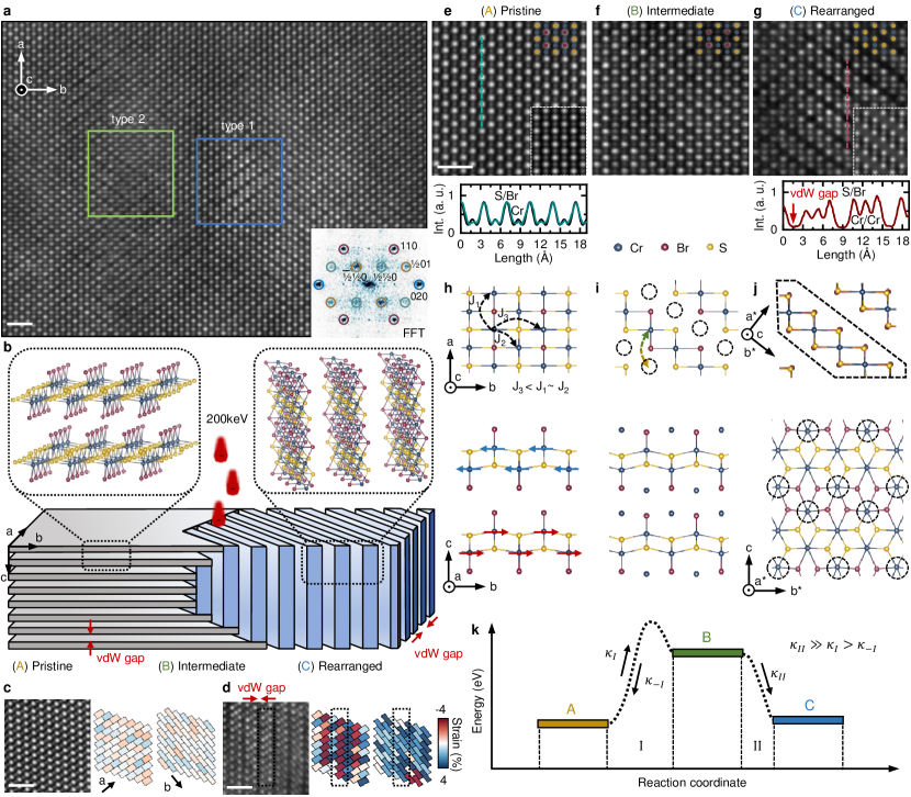
Local Crystal Phase Change. We first demonstrate the electron beam-induced structural rearrangement. Fig. 1a shows a scanning transmission electron microscopy high-angle annular dark-field (STEM-HAADF) image of a typical multilayer CrSBr crystal area after electron beam irradiation (See also Extended Data Figs. 1, 2 and 3). We observe two different types of new structures: type 1 (Supplementary Video 1) is the newly formed in-plane stacked 2D material, while type 2 (Supplementary Video 2) represents a layer stacking fault that forms due to a buildup of strain and potential local loss of Br (discussed in detail in the Extended Data Figs. 8, 9 and 15). We focus on structure type 1 throughout the remainder of this manuscript.
The local beam-induced structural rearrangement of the CrSBr crystal is illustrated in Fig. 1b. Dosing pristine CrSBr (A) with electrons results in the reversible migration of Cr atoms into the vdW gap to form a metastable intermediate crystal state (B) that eventually nucleates into a new magnetic (see below) 2D material (C) that is stacked along the in-plane direction. This striking rearrangement opens a vdW gap in the --plane. While for pristine CrSBr we find lattice distances of and , the vdW gap of the new structure is clearly visible from changes in lattice distances in the - and -direction as evidenced from strain maps of pristine (Fig. 1c) and fully arranged CrSBr (Fig. 1d) obtained from S/Br atom column positions. Generally, even pristine CrSBr crystals exhibit a large variation of up to over wide areas, likely due to the layered nature of the material (see Extended Data Fig. 5, 7 and 9 for detailed analysis of lattice distances and strain). A similar elongation along the -direction is also observed in Li-intercalated FeOCl. [38, 39]
High-magnification STEM-HAADF images of the three different states (A, B and C) are shown in Fig. 1e-g along with their corresponding top- and side-view crystal structure models in Fig. 1h-j. To our advantage, in pristine CrSBr, columns containing S/Br and Cr atoms are spatially well separated in a top-view perspective along the -direction and can be easily distinguished by their image contrast difference, in excellent agreement with the multislice simulations (see inset Fig. 1e). The intensity variation of the atomic columns is also visible in the line profile in Fig. 1g yielding a contrast of . Irradiating with electrons creates a local and intermediate crystal phase (Fig. 1f) visible from local intensity variations of the Cr atom column intensities which over a total of of exposure spontaneously rearranges into the new in-plane stacked 2D material (Fig. 1g).
The electron beam-driven mechanism of this structural rearrangement is described in a reaction coordinate diagram in Fig. 1k. Local irradiation disrupts the bonding structure of Cr atoms, overcoming the activation energy such that the Cr can migrate into the vdW gap with a rate . This state is the local metastable intermediate state (B) (see Fig. 1f and j). From this state, Cr can either reverse to its original position with a rate or irreversibly relax in the stable final rearranged state (C) at a rate . The top- and side-view of the newly formed 2D material is shown in Fig. 1j. Cr atoms from every second diagonal migrate into a proximal diagonal. From the side-view along the direction of a single new 2D layer (highlighted in Fig. 1j), it is apparent that the migrated Cr atoms (see dashed circles) are bonded to four Br and two S atoms instead of the initial two Br atoms and four S atoms. The new crystal symmetry is similar to a 1T phase of CrBr2. [40] The experimental observation is in excellent agreement with the multislice simulated STEM image from the ab initio relaxed structure model. The corresponding change in contrast can also directly be observed in the line cuts along the -direction showing the net loss and surplus of Cr atoms in alternating Cr atom columns, clear evidence for the rearrangement and emergence of the new 2D material. Moreover, the change in the - and -directions is also in excellent agreement between experiment (Fig. 1c and d) and our relaxed ab initio DFT crystallographic model. We find that the ratio between experimental (theoretical) - and -directions increases from 1.3553 (1.3596) to 1.3946 (1.3834).
Nucleation Kinetics. We are particularly motivated by the possibility of forming these structural modifications within a matrix of the naturally grown structure because we can then utilize the spin structures of both structural domains to engineer low-dimensional chiral and/or topological spin textures at their interface. In order to analyze the time evolution of the process described in Fig. 1k more quantitatively, we collect a sequence of STEM-HAADF images at a frame rate of frames/s (total of ) and an electron energy of with a dose of . The complete time evolution of the lattice rearrangement is shown in Fig. 2a.
Selected STEM-HAADF images for , , , , and are shown in Fig. 2b. Since the atom column intensity (image contrast) follows the dependence ( is the atomic number of each element with the number of atoms ), we can track column intensities to directly infer changes in atom column stochiometry as a function of time. Column intensity maps obtained from a Voronoi tesselation of Cr and S/Br (Voronoi diagrams) are shown in Fig. 2c and d (see Extended Data Figs. 4 and 10 for details on the analysis).
While both the Cr Voronoi diagram and the real space STEM-HAADF image reflect the time evolution of the rearranged structure, the S/Br atom columns do not exhibit such a redistribution of intensity over this time frame. Importantly, as the crystal undergoes rearrangement, there is no large change in overall stochiometry (see Fig. 2f) but Cr atoms from diagonals (see dashed black lines 1, 3 and 5 in Fig. 2c at ) migrate to proximal diagonals (orange dashed lines 2 and 4). The migration becomes even more apparent by tracking the average intensity of the two different Cr diagonals as shown in Fig. 2g. For , a splitting of the intensities occurs, a direct consequence of the electron beam-induced Cr migration. The striking migration of Cr in CrSBr is also further demonstrated by the filling of patterned 1D Cr vacancy line defects under irradiation (see Extended Data Fig. 16 and Supplementary Videos 3 and 4, respectively).
To study the nucleation kinetics and crystal rearrangement in space and time, we analyze Cr Voronoi cell intensities from Fig. 2c using the next nearest neighbor Cr atom columns along the two different diagonals (see inset Fig. 2h and Extended Data Fig. 11 for details). This analysis is sensitive to both local and global changes in the CrSBr nucleation kinetics. The spatial distribution of nucleation () at different times is shown in the corresponding nucleation maps (Fig. 2e). Moreover, we derive and summarize the full time evolution from the integrated value of the nucleation maps (degree of nucleation) as shown in Fig. 2h, which represents a precise measure on the degree of rearrangement along one diagonal or the other.
At the CrSBr is pristine (A) with a homogeneous distribution of Cr atom column intensities. However, for the degree of nucleation monotonically increases, reflecting local stochastic nucleation events of the Cr rearrangement (meta-stable state B) that is driven by the electron beam irradiation. Such events spatially appear as high values in the nucleation maps. For a sudden global Cr rearrangement propagates through the analyzed area and the crystal fully rearranges into its final state (C). The full global rearrangement occurs on short time-scales (). We observe the same trend in reciprocal space (see Extended Data Fig. 12). Moreover, aligning the scan-direction (e.g. along the [110] direction) manifests in an additional degree of freedom to control the preferred rearrangement direction (see Extended Data Fig. 3).
To further understand what microscopically triggers the sudden rearrangement, we quantify the time evolution of the net strain in the crystal along the - and -directions (see Fig. 2i and further details on the analysis in the Extended Data Fig. 13). For the -direction, the overall increase is less than , which is due to the compensation of small and large strain values from the alternating lattice distortion within each newly formed 2D layer and the opening of the vdW gap (see Fig. 1d). However, in the -direction for , we observe a continuous buildup of net strain that is accompanied by an increase in local nucleation (Cr migration events). A striking observation is that the net strain decreases simultaneously with the global rearrangement into the new 2D material. We interpret this as the lattice reaching a critical strain value due to the increased number of local Cr migration events that, in order to minimize its free energy, fully relaxes into the rearranged lattice structure (C) to release its accumulated strain.
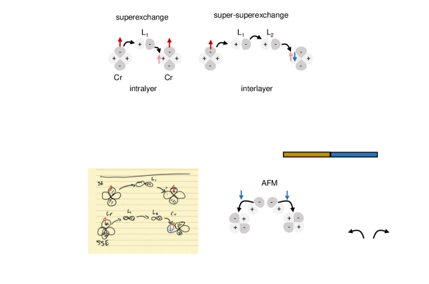
Electronic Structure and Magnetic Interactions. To elucidate the electronic and magnetic properties of the rearranged structure, we calculate the electronic band structure and determine the magnetic interactions from a simplified tight-binding model of the relevant orbitals. Fig. 3a and b show the full Brillouin zone of the pristine and rearranged CrSBr and their corresponding DFT calculated spin-polarized band structures for the essential high symmetry points are shown in Fig. 3c and d. The lowest energy bands of the rearranged CrSBr are fully spin polarized with a direct gap transition at the point and an energy comparable to the pristine CrSBr suggesting a FM ground state. Since we are interested in the magnetic ordering of the rearranged CrSBr and in the spin texture the local rearrangement creates, we further determine the intralayer and interlayer exchange interaction for the pristine and the rearranged CrSBr. For our consideration we determine the intralayer exchange interaction using superexchange mediated by the ligand and the interlayer interaction by super-superexchange via two ligands (see Fig. 3e). By performing strong-coupling perturbation theory (see Fig. 3e,f) using the effective hoppings and crystal-field splittings extracted from spin-unpolarized ab initio band structure calculations, we indeed find the in-plane superexchange interaction is ferromagnetic, with a coordination and unit-cell averaged superexchange of order of for typical correlation parameters (here a minus sign indicates ferromagnetism).
We also compute the interlayer magnetic interactions via the super-superexchange mechanism. Owing to the large separation between layers and roughly linear bond-angle, we find that the interlayer coupling is weakly antiferromagnetic, with a typical value being of order . We therefore expect that for a relatively large range of temperatures the system exhibits quasi-two dimensional ferromagnetism, which is locally well-formed within the planes but only weakly coupled between the planes, creating unusual spin textures in interfaces between rearranged and pristine CrSBr (see Fig. 3g).
Note that, given the quasi-two dimensional nature of the rearranged structure, it is also important to determine the magnetocrystalline anisotropies, which arise from the spin-orbit corrections to superexchange. We can roughly estimate their size [41, 42] as follows. Bromine has the largest atomic spin-orbit coupling, with [41]. This enters into the superexchange correction via second-order perturbation theory with a suppression by , implying that the anisotropic exchange interactions should be of order , which is comparable to the interlayer exchange . We therefore expect that the true form of the magnetic ordering will be determined by a combination of the interlayer antiferromagnetism and in-plane anisotropies, and a more thorough analysis would be the subject of future calculations.
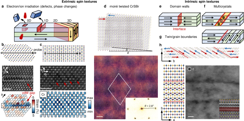
Writing Spin Textures On-Demand. The above calculations show that complex spin textures can be obtained by inserting, through targeted irradiation, regions of the new structure into a CrSBr matrix. The structural amenability of CrSBr provides a wide range of opportunities to program a variety of extrinsic spin textures into the lattice with a range of different topologies (0-3D) (see Fig. 4a). To emphasize this point, we also demonstrate the flexibility of CrSBr for writing additional atom level structural modifications. Fig. 4b shows a representative example of monitoring the scanning direction of the electron probe to selectively create a single Cr line vacancy, which artificially introduces a vertical vdW gap (see Fig. 4b) within the horizontally vdW-bonded matrix. The absence of Cr atoms in the STEM-HAADF image and the formation of a vdW gap from the local strain analysis suggest the feasibility of modifying the crystal structure, and hence magnetic properties, on demand at the atomic scale. Scanning the electron probe across both S-Br and Cr atom columns creates a zig-zag pattern due to the selective migration of Cr atoms when the probe is on a Cr site. This is further shown by the variation in the analysed Cr atom column intensity. Another example for an extrinsic spin texture is the intentional introduction of a twist between two CrSBr sheets to create a superlattice (see Fig. 4d). Twisted magnets are of particular interest for creating exotic quantum magnetic phases. [43] Beyond the intentionally created textures are also intrinsic spin textures that can naturally occur and by themselves represent exciting magnetic systems given the layered nature of the host material. Examples include domain walls, multicrystals and twin and grain boundaries (see Fig. 4e-g). Indeed, we observe examples of twin boundaries with a few width within exfoliated bulk crystals (see Fig. 4h and Extended Fig. 14) creating atomically defined interfaces with different magnetic anisotropy on either side.
Outlook. We believe that these results lay the groundwork for creating and studying new structural phases and related spin textures in vdW materials on the atomic scale. Channel thicknesses of locally rearranged magnetic layers are shorter than state-of-the-art silicon transistor gate lengths, opening up exciting avenues for realizing new spintronic device designs combining out-of-plane and in-plane stacked 2D materials. Similarly, local writing of magnetic textures can be harnessed to controllably generate topological non-trivial spin textures with an unprecedented degree of control over dimensionality. Moreover, the intricate interplay of magnetization and localization effects of excitons will be interesting for future investigation, potentially leading to engineering spin-Hamiltonians in situ.
The atomic level control demonstrated here will also be critical in a mechanistic understanding of proximity-induced effects in low dimensional heterostructures. Finally, magnetic and spin-orbit degrees of freedom in 2D magnets allow for flexible interaction engineering as well as simultaneous control of electronic band structure and topology, essential towards realizing universal classes of quantum many-body Hamiltonians and using vdW heterostructures as programmable quantum simulation platforms.
I Acknowledgements
J.K. acknowledges support by the Alexander von Humboldt foundation. T.P. and F.M.R. acknowledge the funding from the U.S. Department of Energy, Office of Basic Energy Sciences, Division of Materials Sciences and Engineering under Award DE-SC0019336 for STEM characterization. J.D.T. acknowledges support from Independent Research Fund Denmark through grant no. 9035-00006B. Work by J.B.C. and P.N. is partially supported by the Quantum Science Center (QSC), a National Quantum Information Science Research Center of the U.S. Department of Energy (DOE). J.B.C. is an HQI Prize Postdoctoral Fellow and gratefully acknowledges support from the Harvard Quantum Initiative. P.N. is a Moore Inventor Fellow and gratefully acknowledges support through Grant GBMF8048 from the Gordon and Betty Moore Foundation. M.L, M.F., A.S. and F.J. were supported by the Deutsche Forschungsgemeinschaft (DFG) within RTG 2247 and through a grant for CPU time at the HLRN (Berlin/Göttingen). R.A.W. was supported by the Arnold O. Beckman Fellowship in Chemical Sciences. Z.S. and J.L. were supported by Czech Science Foundation (GACR No. 20-16124J).
II Author contributions
J.K. and F.M.R. conceived and designed the experiments, J.D.T. and J.K. prepared the samples for electron microscopy, T.P. collected STEM data, J.K. wrote the scripts and analyzed the data, J.K., performed the optical measurements, R.A.W. contributed modelling the crystal structure, Z.S. and J.L. synthesized high-quality bulk CrSBr crystals, J.B.C. and P.N. computed the magnetic properties, M.L., M.F., A.S. and F.J. performed DFT calculations, J.K. wrote the manuscript with input from all co-authors.
III Methods
III.1 Crystal synthesis
CrSBr crystals were prepared by direct reaction from elements. Chromium (99.99%, -60 mesh, Chemsavers, USA), bromine (99.9999%, Sigma-Aldrich, Czech Republic) and sulfur (99.9999%, Stanford Materials, USA) were mixed in stochiometric ratio in a quartz ampoule (35x220mm) corresponding to 15g of CrSBr. Bromine excess of 0.5g was used to enhance vapor transport. The material was pre-reacted in an ampoule using a crucible furnace at 700 °C for 12 hours, while the second end of the ampoule was kept below 250 °C. The heating procedure was repeated two times until the liquid bromine disappeared. The ampoule was placed in horizontal two zone furnace for crystal growth. First the growth zone was heated on 900 °C, while the source zone was heated on 700 °C for 25 hours. For the growth the thermal gradient was reversed and the source zone was heated from 900 °C to 940 °C and growth zone from 850 °C to 800°C over a period of 7 days. The crystals with dimensions up to 5x20 mm were removed from ampule in an Ar glovebox.
III.2 Structural characterization of bulk CrSBr
We characterized grown CrSBr bulk crystals using SEM, EDS, XPS and XRD (see Extended Figs. 17, 18 and 19). The EDS data show homogeneous distribution of Cr, S and Br. High-resolution XPS reveals the presence of Br- and S2- anions and the Cr primarily in the oxidation state. The X-ray diffraction reveals a pure single phase CrSBr with a high preferential orientation owing to the layered vdW structure.
III.3 Sample fabrication
Bulk CrSBr flakes are exfoliated using the Scotch tape method. Individual flakes and their thickness are determined by atomic force microscopy (AFM) and optical phase contrast. Exfoliated flakes were transferred to TEM compatible sample grids using cellulose acetate butyrate (CAB) as polymer handle. [44] The CAB was then dissolved in acetone and the TEM grids rinsed in isopropanol before critical point drying. Twisted CrSBr samples are fabricated using the dry viscoelastic transfer method.
III.4 Optical spectroscopy
We optically characterized the CrSBr bulk crystal by Raman and photoluminescence (PL) spectroscopy at room temperature (see Extended Fig. 19). The PL spectrum of a multilayer CrSBr flake is measured exciting at with an excitation power of . For the Raman data, we used a low-frequency filter set to obtain both, Stokes and Anti-Stokes Raman modes. A monochromatic laser excitation at was used at a power of .
III.5 STEM imaging
STEM imaging was performed with a probe-corrected Thermo Fisher Scientific Themis Z G3 - S/TEM operated at and with the probe convergence semi-angle of 19 mrad and 30 mrad, respectively. The beam current was varied between - to explore electron dosing conditions. A collection semi-angle of 63-200 mrad was used for HAADF STEM imaging.
III.6 STEM data analysis
In order to analyze sequences of STEM-HAADF images, movies are drift corrected before subsequent data processing. After drift correction, the position of the S/Br atom columns are determined by using atom-column indexing. [45] Since Cr atom column intensities change throughout the video due to the Cr migration, we use the positions of proximal S/Br atom columns in order to approximate the Cr atom column position. Based on each set of x-y-coordinates from both, S/Br and Cr atom columns, we perform a Voronoi tesselation. Each Voronoi cell represents a single atom column. In order to obtain the atom column intensity, we integrate the intensity in the original STEM-HAADF image by masking out a polygon defined by each individual Voronoi cell. To determine local bond distances, we determine the distance between S/Br atom columns along the different crystallographic directions. Corresponding details are provided in Extended Figs. 4, 5, 6 and 7.
III.7 STEM multislice simulation
STEM multislice simulations were performed on DFT relaxed crystal structure of the pristine and rearranged CrSBr using the Dr. Probe software. We used simulation parameters similar to the experimental conditions, including beam energy, convergence angle and collection angle, as well as the sample thickness. Simulated HAADF images were convolved with a Gaussian kernel with full-width at half-maximum of to approximately account for the finite size of the effective electron source.
III.8 Ab initio calculations
The ab initio calculations were performed using density functional theory (DFT), using the Vienna ab initio simulation package (VASP) and the projected augmented wave method [46, 47]. Bulk (vertical) structures were modelled with supercells containing 6 (12) atoms. The atomic and electronic structures were determined using the PBE functional. Van-der-Waals corrections were added in the Tkatchenko-Scheffler approximation [48]. A plane wave basis with an energy cutoff of and a (7 × 5 × 2) ((2 × 4 × 4)) Monkhorst-Pack-point sampling has been employed for the bulk (vertical) structure. Structural relaxations were performed until the forces were smaller than . To generate the TB Hamiltonian, used in the spin-wave theory, the Wannier90 package [49] was employed.
III.9 Magnetic Structure
We predict the form of the magnetic structure by applying standard superexchange theory. We model the onsite energy levels, including electron-electron interactions, by a Hubbard-Kanamori + crystal-field Hamiltonian [50] which in the rotationally invariant limit assumes the form
| (1) |
with Hubbard- modeling Coulomb repulsion, Hund’s intra-atomic exchange which favors highest spin multiplicity, and single-particle crystal-field splitting . Here we have introduced -bands electronic operators which measure the total number of -electrons in crystal-field level , the total -electron occupation, and total spin of the Cr ion on site , respectively. The neglect of terms due to rotational symmetry breaking is a crude approximation, but partly justified by the small crystal-field splittings. Following Ref. 33, we compute the exchange for a range of values of and . We obtain the crystal-field splittings from the ab initio calculations.
We determine the superexchange energies by performing strong-coupling perturbation theory up to second order in the effective hoppings. See Ref. 51 for a similar treatment in the case of CrI3 and CrCl3, and also Ref. 52. For a dimer of Cr ions in the configuration, we find the superexchange interaction by computing , which assumes that the spin-interactions are a simple invariant (this is guaranteed in the absence of spin-orbit coupling) Heisenberg form, and FM and AFM indicate the states and , respectively. In terms of the orbitally-resolved hoppings from orbital on site 1 to orbital on site 2, and vice-versa, we find the result
| (2) |
where is the energy of the excitation and is the occupation of the level and is taken to be 1 for the lower three levels and 0 for the upper two levels.
The final ingredient is to derive the effective ligand-mediated hoppings which we approximate by
| (3) |
where the product is understood as a matrix product over the intermediate orbital states, and sums over the participating ligands (for edge sharing octahedra, there are two). Here, is the on-site ligand- block of the Wannier Hamiltonian, and are the appropriate Cr-ligand hybridizations, also obtained from wannierized ab initio calculations. We find that, except for extreme values of the Hubbard- and Hund’s-, the intra-layer exchanges are robustly FM.
In order to fix the interlayer ordering, we must compute the interlayer super-superexchange interactions. In this case, we again apply Eqn. 1, but now using (alongside the direct -band hoppings) the effective -band hoppings of
| (4) |
with labeling all participating pairs of ligands. We find that this produces a weak AFM interlayer exchange , as in the pristine case but now with a re-oriented magnetic structure.
IV Additional information
IV.1 Supplementary Information
A detailed SI accompanies this paper along with electron microscopy videos.
IV.2 Data availability
The data that support the findings of this study are available from the corresponding author on reasonable request.
IV.3 Code availability
The codes used for data analysis as well as ab initio calculations are available from the corresponding author on reasonable request.
IV.4 Competing financial interests
The authors declare no competing financial interests.
References
- [1] Žutić, I., Fabian, J. & Sarma, S. D. Spintronics: Fundamentals and applications. Reviews of Modern Physics 76, 323–410 (2004). URL https://doi.org/10.1103/revmodphys.76.323.
- [2] Huang, B. et al. Layer-dependent ferromagnetism in a van der Waals crystal down to the monolayer limit. Nature 546, 270–273 (2017). URL http://www.nature.com/articles/nature22391.
- [3] Gong, C. et al. Discovery of intrinsic ferromagnetism in two-dimensional van der Waals crystals. Nature 546, 265–269 (2017). URL http://www.nature.com/articles/nature22060.
- [4] Deng, Y. et al. Gate-tunable room-temperature ferromagnetism in two-dimensional Fe3GeTe2. Nature 563, 94–99 (2018). URL http://www.nature.com/articles/s41586-018-0626-9.
- [5] Burch, K. S., Mandrus, D. & Park, J.-G. Magnetism in two-dimensional van der Waals materials. Nature 563, 47–52 (2018). URL http://www.nature.com/articles/s41586-018-0631-z.
- [6] Ising, E. Beitrag zur theorie des ferromagnetismus. Zeitschrift für Physik 31, 253–258 (1925). URL https://doi.org/10.1007/bf02980577.
- [7] Bethe, H. Zur theorie der metalle. Zeitschrift für Physik 71, 205–226 (1931). URL https://doi.org/10.1007/bf01341708.
- [8] Lieb, E., Schultz, T. & Mattis, D. Two soluble models of an antiferromagnetic chain. Annals of Physics 16, 407–466 (1961). URL https://doi.org/10.1016/0003-4916(61)90115-4.
- [9] Mermin, N. D. & Wagner, H. Absence of Ferromagnetism or Antiferromagnetism in One- or Two-Dimensional Isotropic Heisenberg Models. Physical Review Letters 17, 1133–1136 (1966). URL https://link.aps.org/doi/10.1103/PhysRevLett.17.1133.
- [10] Hohenberg, P. C. Existence of long-range order in one and two dimensions. Physical Review 158, 383–386 (1967). URL https://doi.org/10.1103/physrev.158.383.
- [11] Basov, D. N., Averitt, R. D. & Hsieh, D. Towards properties on demand in quantum materials. Nature Materials 16, 1077–1088 (2017). URL https://doi.org/10.1038/nmat5017.
- [12] Narang, P., Garcia, C. A. C. & Felser, C. The topology of electronic band structures. Nature Materials 20, 293–300 (2020). URL https://doi.org/10.1038/s41563-020-00820-4.
- [13] Song, T. et al. Giant tunneling magnetoresistance in spin-filter van der waals heterostructures. Science 360, 1214–1218 (2018). URL https://doi.org/10.1126/science.aar4851.
- [14] Kim, H. H. et al. One million percent tunnel magnetoresistance in a magnetic van der waals heterostructure. Nano Letters 18, 4885–4890 (2018). URL https://doi.org/10.1021/acs.nanolett.8b01552.
- [15] Wang, Z. et al. Tunneling spin valves based on fe3gete2/hBN/fe3gete2 van der waals heterostructures. Nano Letters 18, 4303–4308 (2018). URL https://doi.org/10.1021/acs.nanolett.8b01278.
- [16] Klein, D. R. et al. Probing magnetism in 2d van der waals crystalline insulators via electron tunneling. Science 360, 1218–1222 (2018). URL https://doi.org/10.1126/science.aar3617.
- [17] Jiang, S., Li, L., Wang, Z., Shan, J. & Mak, K. F. Spin tunnel field-effect transistors based on two-dimensional van der waals heterostructures. Nature Electronics 2, 159–163 (2019). URL https://doi.org/10.1038/s41928-019-0232-3.
- [18] Song, T. et al. Voltage control of a van der waals spin-filter magnetic tunnel junction. Nano Letters 19, 915–920 (2019). URL https://doi.org/10.1021/acs.nanolett.8b04160.
- [19] Huang, B. et al. Electrical control of 2D magnetism in bilayer CrI3. Nature Nanotechnology 13, 544–548 (2018). URL http://www.nature.com/articles/s41565-018-0121-3.
- [20] Jiang, S., Shan, J. & Mak, K. F. Electric-field switching of two-dimensional van der Waals magnets. Nature Materials 17, 406–410 (2018). URL http://www.nature.com/articles/s41563-018-0040-6.
- [21] Jiang, S., Li, L., Wang, Z., Mak, K. F. & Shan, J. Controlling magnetism in 2d CrI3 by electrostatic doping. Nature Nanotechnology 13, 549–553 (2018). URL https://doi.org/10.1038/s41565-018-0135-x.
- [22] Muhlbauer, S. et al. Skyrmion lattice in a chiral magnet. Science 323, 915–919 (2009). URL https://doi.org/10.1126/science.1166767.
- [23] Yu, X. Z. et al. Real-space observation of a two-dimensional skyrmion crystal. Nature 465, 901–904 (2010). URL https://doi.org/10.1038/nature09124.
- [24] Romming, N. et al. Writing and deleting single magnetic skyrmions. Science 341, 636–639 (2013). URL https://doi.org/10.1126/science.1240573.
- [25] Yu, X. Z. et al. Near room-temperature formation of a skyrmion crystal in thin-films of the helimagnet FeGe. Nature Materials 10, 106–109 (2010). URL https://doi.org/10.1038/nmat2916.
- [26] Li, Z.-A. et al. Magnetic skyrmion formation at lattice defects and grain boundaries studied by quantitative off-axis electron holography. Nano Letters 17, 1395–1401 (2017). URL https://doi.org/10.1021/acs.nanolett.6b04280.
- [27] Matsumoto, T. et al. Direct observation of 7 domain boundary core structure in magnetic skyrmion lattice. Science Advances 2, e1501280 (2016). URL https://doi.org/10.1126/sciadv.1501280.
- [28] Jin, C. et al. Control of morphology and formation of highly geometrically confined magnetic skyrmions. Nature Communications 8 (2017). URL https://doi.org/10.1038/ncomms15569.
- [29] Duine, R. A., Lee, K.-J., Parkin, S. S. P. & Stiles, M. D. Synthetic antiferromagnetic spintronics. Nature Physics 14, 217–219 (2018). URL https://doi.org/10.1038/s41567-018-0050-y.
- [30] Lin, Y.-C., Dumcenco, D. O., Huang, Y.-S. & Suenaga, K. Atomic mechanism of the semiconducting-to-metallic phase transition in single-layered MoS2. Nature Nanotechnology 9, 391–396 (2014). URL https://doi.org/10.1038/nnano.2014.64.
- [31] Katscher, H. & Hahn, H. Über chalkogenidhalogenide des dreiwertigen chroms. Die Naturwissenschaften 53, 361–361 (1966). URL https://doi.org/10.1007/bf00621875.
- [32] Göser, O., Paul, W. & Kahle, H. Magnetic properties of CrSBr. Journal of Magnetism and Magnetic Materials 92, 129–136 (1990). URL https://doi.org/10.1016/0304-8853(90)90689-n.
- [33] Wang, C. et al. A family of high-temperature ferromagnetic monolayers with locked spin-dichroism-mobility anisotropy: MnNX and CrCX (x=cl, br, i; c=s, se, te). Science Bulletin 64, 293–300 (2019). URL https://doi.org/10.1016/j.scib.2019.02.011.
- [34] Wang, H., Qi, J. & Qian, X. Electrically tunable high curie temperature two-dimensional ferromagnetism in van der waals layered crystals. Applied Physics Letters 117, 083102 (2020). URL https://doi.org/10.1063/5.0014865.
- [35] Telford, E. J. et al. Layered antiferromagnetism induces large negative magnetoresistance in the van der waals semiconductor CrSBr. Advanced Materials 32, 2003240 (2020). URL https://doi.org/10.1002/adma.202003240.
- [36] Lee, K. et al. Magnetic order and symmetry in the 2d semiconductor CrSBr. Nano Letters (2021). URL https://doi.org/10.1021/acs.nanolett.1c00219.
- [37] Wilson, N. P. et al. Interlayer electronic coupling on demand in a 2d magnetic semiconductor. arXiv (2021). eprint arXiv:2103.13280.
- [38] Palvadeau, P., Coic, L., Rouxel, J. & Portier, J. The lithium and molecular intercalates of FeOCl. Materials Research Bulletin 13, 221–227 (1978). URL https://doi.org/10.1016/0025-5408(78)90226-x.
- [39] Beck, J. Über chalkogenidhalogenide des chroms synthese, kristallstruktur und magnetismus von chromsulfidbromid, CrSBr. Zeitschrift für anorganische und allgemeine Chemie 585, 157–167 (1990). URL https://doi.org/10.1002/zaac.19905850118.
- [40] Kulish, V. V. & Huang, W. Single-layer metal halides MX2 (x = cl, br, i): stability and tunable magnetism from first principles and monte carlo simulations. Journal of Materials Chemistry C 5, 8734–8741 (2017). URL https://doi.org/10.1039/c7tc02664a.
- [41] Tartaglia, T. A. et al. Accessing new magnetic regimes by tuning the ligand spin-orbit coupling in van der Waals magnets. Science Advances 6, eabb9379 (2020). eprint 2007.12818.
- [42] Stavropoulos, P. P., Liu, X. & Kee, H.-Y. Magnetic anisotropy in spin-3/2 with heavy ligand in honeycomb Mott insulators: Application to CrI3. Physical Review Research 3, 013216 (2021). eprint 2009.04475.
- [43] Hejazi, K., Luo, Z.-X. & Balents, L. Noncollinear phases in moiré magnets. Proceedings of the National Academy of Sciences 117, 10721–10726 (2020). URL https://doi.org/10.1073/pnas.2000347117.
- [44] Thomsen, J. D., Kling, J., Mackenzie, D. M. A., Bøggild, P. & Booth, T. J. Oxidation of suspended graphene: Etch dynamics and stability beyond 1000 °c. ACS Nano (2019). URL https://doi.org/10.1021/acsnano.8b08979.
- [45] Sang, X., Oni, A. A. & LeBeau, J. M. Atom column indexing: Atomic resolution image analysis through a matrix representation. Microscopy and Microanalysis 20, 1764–1771 (2014). URL https://doi.org/10.1017/s1431927614013506.
- [46] Blöchl, P. E. Projector augmented-wave method. Phys. Rev. B 50, 17953–17979 (1994). URL https://link.aps.org/doi/10.1103/PhysRevB.50.17953.
- [47] Kresse, G. & Joubert, D. From ultrasoft pseudopotentials to the projector augmented-wave method. Phys. Rev. B 59, 1758–1775 (1999). URL http://link.aps.org/doi/10.1103/PhysRevB.59.1758.
- [48] Tkatchenko, A. & Scheffler, M. Accurate molecular van der waals interactions from ground-state electron density and free-atom reference data. Phys. Rev. Lett. 102, 073005 (2009). URL https://link.aps.org/doi/10.1103/PhysRevLett.102.073005.
- [49] Pizzi, G. et al. Wannier90 as a community code: new features and applications. Journal of Physics: Condensed Matter 32, 165902 (2020). URL https://doi.org/10.1088%2F1361-648x%2Fab51ff.
- [50] Georges, A., de’ Medici, L. & Mravlje, J. Strong Correlations from Hund’s Coupling. Annu. Rev. Condens. Matter Phys. 4, 137 (2013).
- [51] Besbes, O., Nikolaev, S., Meskini, N. & Solovyev, I. Microscopic origin of ferromagnetism in the trihalides CrCl3 and CrI3. Phys. Rev. B 99, 104432 (2019).
- [52] Huang, C. et al. Toward Intrinsic Room-Temperature Ferromagnetism in Two-Dimensional Semiconductors. Journal of the American Chemical Society 140, 11519–11525 (2018).