Valley-Polarized Quantum Anomalous Hall Phase in Bilayer Graphene
with Layer-Dependent Proximity Effects
Abstract
Realizations of some topological phases in two-dimensional systems rely on the challenge of jointly incorporating spin-orbit and magnetic exchange interactions. Here, we predict the formation and control of a fully valley-polarized quantum anomalous Hall effect in bilayer graphene, by separately imprinting spin-orbit and magnetic proximity effects in different layers. This results in varying spin splittings for the conduction and valence bands, which gives rise to a topological gap at a single Dirac cone. The topological phase can be controlled by a gate voltage and switched between valleys by reversing the sign of the exchange interaction. By performing quantum transport calculations in disordered systems, the chirality and resilience of the valley-polarized edge state are demonstrated. Our findings provide a promising route to engineer a topological phase that could enable low-power electronic devices and valleytronic applications as well as putting forward layer-dependent proximity effects in bilayer graphene as a way to create versatile topological states of matter.
Topological phases of matter hold great potential in a myriad of fields such as low-power electronics, spintronics, sensing, metrology or quantum information processing Nayak et al. (2008); Hasan and Kane (2010); Qi and Zhang (2011); Ren et al. (2016); Liu et al. (2016). The quantum anomalous Hall effect (QAHE) is one of such phases Haldane (1988); Ohgushi et al. (2000); Onoda and Nagaosa (2003), displaying dissipationless chiral edge states, quantized Hall conductivity and finite Chern number at zero external magnetic field Thouless et al. (1982); Hatsugai (1993). Since topological currents are extremely robust to disorder effects Hasan and Kane (2010), they constitute a very attractive platform for ultralow power electronics. Many materials can host the QAHE, such as semiconductor quantum wells Liu et al. (2008); Wang et al. (2014), graphene Qiao et al. (2010); Tse et al. (2011); Ding et al. (2011); Qiao et al. (2012); Offidani and Ferreira (2018); Högl et al. (2020) and other two-dimensional systems Ezawa (2012); Zou et al. (2020), or more recently magnetic topological insulators Yu et al. (2010); Chang et al. (2013); Bestwick et al. (2015); Otrokov et al. (2019); Tokura et al. (2019); Deng et al. (2020) and twisted bilayer graphene Serlin et al. (2020); Chen et al. (2020); Polshyn et al. (2020); Tschirhart et al. (2021). Among the vast playground of quantum materials Giustino et al. (2021), graphene-based compounds are very promising due to their chemical stability, multiple degrees of freedom (lattice, spin, valley), ease of device fabrication and scalability as well as the possibility to combine them with other materials to form van der Waals heterostructures Geim and Grigorieva (2013); Sierra et al. (2021). Unfortunately, the main ingredient of the QAHE is the coexistence of spin-orbit coupling (SOC) and magnetism Ren et al. (2016); Liu et al. (2016), and these effects are generally very small or absent in graphene-based devices. Accordingly, engineering these interactions via proximity effects Žutić et al. (2019); Huang et al. (2020) has been a major focus during the last decade Garcia et al. (2018); Roche et al. (2015); Yang et al. (2013); Hallal et al. (2017); Wang et al. (2015); Wei et al. (2016); Singh et al. (2017); Leutenantsmeyer et al. (2017); Karpiak et al. (2019); Gmitra and Fabian (2015); Gmitra et al. (2016); Jin and Jhi (2013); Song et al. (2018); Benitez et al. (2018); Ghiasi et al. (2017); Khokhriakov et al. (2018); Karpiak et al. (2019). Nevertheless, while adding either SOC or exchange has been reported experimentally (with characteristic spin splittings and spin textures), imprinting both effects simultaneously and achieving a measurable QAHE still remains a tantalizing challenge. This would require encapsulating graphene between a ferromagnetic insulator (FMI) and a strong-SOC material, as proposed recently in Ref. Zollner et al. (2020), or to use a single material that can induce both interactions simultaneously Qiao et al. (2014); Zhang et al. (2015).
In addition to SOC and magnetism, the layer degree of freedom of bilayer graphene (BG) and the possibility to generate a sizable band gap by applying an external perpendicular electric field offers an additional knob to engineer topological phases Tse et al. (2011); Qiao et al. (2013); Alsharari et al. (2018); Island et al. (2019); Zaletel and Khoo (2019); Tiwari et al. (2021a). Unfortunately, the proposed models for realizing the QAHE in bilayer graphene have been limited to some extension of the monolayer graphene case where both layers require SOC and exchange Tse et al. (2011); Qiao et al. (2013). Recently, proximity effects on one of the layers in BG was shown to mainly affect the conduction (or valence) band owing to the layer localization of these low energy states Gmitra and Fabian (2017); Khoo et al. (2017); Zollner et al. (2018); Alsharari et al. (2018); Cardoso et al. (2018); Tiwari et al. (2021b); Ingla-Aynés et al. (2021); McCann and Fal’ko (2006); McCann and Koshino (2013). Accordingly, such effect can be harnessed to add SOC and magnetism separately on each layer by sandwiching BG between SOC and magnetic materials Zollner et al. (2020), as sketched in Fig. 1. In such device configuration, the wave function localization can be reversed by interchanging the interlayer potential with a perpendicular electric field, hence enabling a possible swapping of the induced spin splittings between the conduction and valence bands and therefore modulate the proximity effects.
In this Letter, we take advantage of this layer-dependent proximity effect to predict the formation of a quantum anomalous Hall phase in encapsulated bilayer graphene. By introducing SOC and exchange interactions separately in different layers, the valence and conduction bands hybridize in such a way that a topological gap opens but only at a single Dirac cone, hence resulting in a valley-polarized quantum anomalous Hall effect (VP-QAHE) with Chern number , previously only theorized in silicene Pan et al. (2014, 2015) and in artificial honeycomb lattices Zhou et al. (2017). This proposal of QAHE is likely more experimentally feasible than previous mechanisms Tse et al. (2011); Qiao et al. (2013) since only one interaction per layer is needed, suggesting that heterostructures with common materials such as two-dimensional magnets/BG/transition metal dichalcogenides could be used. We show that the valley-polarization and chirality of the edge states is reversed by changing the sign of the exchange interaction, and that an applied electric field can switch the topological phase. Transport calculations in nonlocal geometries further reveal that the valley-polarized edge states are robust to both bulk and edge disorders. Finally, we argue that the VP-QAHE should be observable with currently employed materials and discuss possible applications.
Our starting point is the tight-binding of bilayer graphene encapsulated between a ferromagnetic insulator and a strong-SOC material (Fig. 1). The Hamiltonian is that of Bernal-stacked BG McCann and Koshino (2013) with SOC and exchange interaction, namely, . The first term is the orbital part . Each term is detailed elsewhere H ; Sup and here we just emphasize that describes an interlayer potential that opens a gap of magnitude at the Dirac point (for ) McCann and Koshino (2013). For we assume the typical terms induced on graphene by a transition metal dichalcogenide Gmitra and Fabian (2015); Gmitra et al. (2016); Kochan et al. (2017) or topological insulators Song et al. (2018); Zollner and Fabian (2021a), which includes Rashba and sublattice-dependent intrinsic SOC:
| (1) |
The first line describes the spin-mixing Rashba SOC with strength , while is a vector of spin Pauli matrices and a unit vector from site to . The other term is the spin-conserving intrinsic SOC with value () if the hopping connects atoms of the sublattice A (B); and if the hopping is counterclockwise (clockwise). We can rewrite the intrinsic SOC as the Kane-Mele SOC Kane and Mele (2005), , and valley-Zeeman SOC Gmitra and Fabian (2015); Gmitra et al. (2016); Kochan et al. (2017), . opens a topological gap at K/K′ valleys whereas produces an exchange field with opposite signs at different valleys. Here, we set as this term is always much smaller than any other parameter Garcia et al. (2018). Finally, the magnetic proximity effect is modeled by the term
| (2) |
where is the magnetization direction of the FMI and the exchange coupling.
The mechanism proposed in this work is illustrated in Fig. 1. Thanks to the layer-dependent proximity effects, the valence band is spin-splitted due to the exchange coupling , while dictates the conduction band splitting (with for K and K′, respectively). For illustration purpose, the system initially presents a finite gap due to a substrate-induced interlayer potential Gmitra and Fabian (2017). Then, tuning the value with a perpendicular electric field allows to reduce such band gap and makes the conduction and valence band overlap. Since the spins of the conduction band minimum and valence band maximum at K′ are identical, the bands interchange but the gap remains nonzero Liu et al. (2008). However, the spins are opposite at the K valley, resulting in a band crossing. Upon the addition of the Rashba SOC, is not a good quantum number anymore due to spins mixing, and the band hybridization yields a gap opening Yu et al. (2010); Qiao et al. (2010). We argue below that this gap is topological and displays the VP-QAHE.
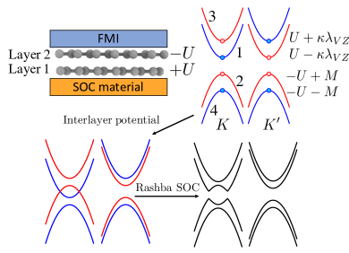
Fig. 2(a) shows the band structure and spin texture near the Dirac cones once the bands have hybridized, noting the usage of large parameters to emphasize the qualitative features of the model, while more realistic parameters are later discussed in relation to experiments (see Fig. 5). To confirm the presence of the QAHE, we compute the Chern number , whose value determines the number of topological edge states and relates to the intrinsic Hall conductivity as Thouless et al. (1982). The quantity is the Berry curvature and for a two-dimensional system equals to Xiao et al. (2010); Yao et al. (2004)
| (3) |
Here, and are band indices, is a Bloch state with energy , is the Fermi-Dirac distribution and is the velocity operator.
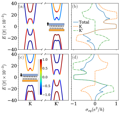
Our system displays nonzero Berry curvature only close to K and K′-points. Consequently, we can perform the integration of the Berry curvature near each valley separately and obtain the valley-resolved Hall conductivity together with its total value; we plot these quantities in Fig. 2(b). In the energies corresponding to the band gap, the total Hall conductivity is quantized at exactly , proving the existence of the QAHE with . Importantly, the valley-resolved conductivities reveal that all the contribution comes only from the K valley, indicating that the gap at K (K′) is topological (trivial) and that the QAHE is valley-polarized. This fact can also be inferred from the spin texture because the component of the spin changes sign abruptly at the anticrossing point of the topological gap.
Furthermore, changing the sign of either or will swap the topology of each valley. Experimentally, is fixed by the interaction of graphene with the substrate, but can be reversed easily by a magnetic field or even by electric means in multiferroic systems Matsukura et al. (2015) or two-dimensional magnets Huang et al. (2018); Jiang et al. (2018); Wang et al. (2018); Johansen et al. (2019). Figs. 2(c) and 2(d) show the bands and Hall conductivity for , respectively. One clearly sees that the band structure is exactly as opposite as that of panel (a), and indeed confirms the opening of the topological gap at K′. Interestingly, not only does the valley polarization of the Hall conductivity change, but also its sign, indicating that the chirality of the edge states is reversed. In contrast, if is kept fixed but it is the sign of that is inverted (not shown), the valley polarization also flips while remains unchanged.
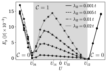
It is not obvious whether the system remains topological if varies and more bands hybridize. Therefore, we study how the topological phase and the band gap value, , depend on the model parameters. For that, it is useful to label the four low-energy bands, as shown by the numbers 1-4 in Fig. 1. Then, assuming the spin splitting induced by exchange is larger than that of SOC, the critical values of that make bands and overlap at K/K′ can be evaluated analytically: , , and . These values are actually approximate because will modify the band dispersion, but they are nevertheless in very good agreement with full numerical calculations. Fig. 3 displays and as a function of for different Rashba strengths. One clearly observes that the topological phase transitions occur only at and . Consequently, the VP-QAHE persists in the range . This entails that increasing the proximity interactions facilitates the range of electric fields needed to access the topological phase. Moreover, the maximum value of the band gap is neither centered at nor is the same for distinct . From the different plots of Fig. 3, it is seen that is proportional to in the topological phase. The scaling is approximately linear in the range of values studied, while larger Rashba SOC leads to sublinear scaling and even gap closing (not shown here) since more strongly distorts the bands, hence invalidating the mechanism described in Fig. 1.
In virtue of the bulk-boundary correspondence, a bulk topological gap implies the existence of edge states in a finite size system. It is thus instructive to scrutinize the band structure of a finite BG sample, as plotted in Fig. 4(a) for a zigzag ribbon of width 25 nm. There are several in-gap states that correspond to edge states Frank et al. (2018); Island et al. (2019). The two pair of crossing bands in the middle of the Brillouin zone are trivial edge states arising from the valley-Zeeman SOC Gmitra et al. (2016); Frank et al. (2018), while the bands in the right valley are also non-topological edge states that appear in a zigzag BG with nonzero Qiao et al. (2011). Differently, the bands inside the gap of the left valley are the ones expected in the QAHE phase, as highlighted by the red color in Fig. 4(a). Therefore, there are at least three propagating modes in the bulk gap, although in principle only one should convey the Hall response. To corroborate this, we carry out quantum transport simulations in a Hall-bar device (inset in Fig. 4(b)) to evaluate the transverse Hall voltage as a response to a longitudinal current met .
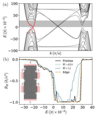
The Hall resistance versus energy is plotted in Fig. 4(b) and shows a clear quantization at in the energy region inside the bulk band gap seen in Fig. 4(a) (shaded gray region). This indicates the presence of a VP-QAHE and confirms that only one state contributes to edge conduction. We note that at energies below the Hall resistance is not quantized (but still finite) because one of the bulk bands overlaps with the edge state, which likely occurs due to the large value of that slightly distorts the bulk band dispersion Ras .
Next, we add static disorder to the Hamiltonian to test the robustness of these states. We introduce (i) bulk Anderson disorder with the term , where is a random potential uniformly distributed at each site , and (ii) edge disorder, which is modeled with two parameters Mucciolo et al. (2009); Caridad et al. (2018): the probability and the number of sweeps, (the resulting disordered edges are depicted in the inset of Fig. 4(b)). For each sweep , a random number is assigned to each atom at the edge of the device and such site is removed if . The several plots in Fig. 4(b) show that both types of disorder do not significantly affect . For bulk disorder, even when the disorder strength is more than 30 times larger than the band gap, the quantization is still resilient in a given energy window. For edge disorder, the effect is minimal even though we use and , which corresponds to having removed on average unit cells on the edges.
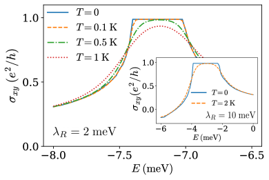
To discuss the possible measurement of VP-QAHE, we plot in Fig. 5 the Hall conductivity for parameters extracted from experiments or ab initio simulations, namely, meV for graphene/transition metal dichalcogenide heterostructures with proper alignment or twist angle Li and Koshino (2019); David et al. (2019); Naimer et al. (2021) and meV for graphene on CrSe Wu et al. (2020) or on CrSBr Ghiasi et al. (2021). The plateau extends over 0.5 meV and is visible below K. For a larger value of the Rashba SOC of 10 meV Island et al. (2019), the effect persists up to 2 K with a plateau width of meV (see inset in Fig. 5).
In this work, the formation of a fully valley-polarized QAHE has been predicted in BG when magnetic and SOC proximity effects are imprinted on different layers. Such topological phase was previously suggested in silicene Pan et al. (2014, 2015) and in Cu-decorated In lattices on Si(111) surfaces Zhou et al. (2017). Bilayer graphene is however more chemically stable and easier to integrate in electronic devices, and it further allows tailoring proximity effects by properly choosing the substrates or twist angles between layers. Additionally, a correlated-induced VP-QAHE has also been observed in several moiré superlattices such as twisted bilayer graphene Serlin et al. (2020), trilayer graphene/hexagonal boron nitride Chen et al. (2020), twisted monolayer/bilayer graphene Polshyn et al. (2020) or twisted bilayer graphene aligned with hexagonal boron nitride Tschirhart et al. (2021). In these systems, the electron correlation appearing at flat bands leads to a valley-polarization that breaks time-reversal symmetry, and together with a large Berry curvature of the valley states, produces a VP-QAHE at some band fillings. This mechanism thus requires strong correlations induced by twisting adjacent layers, while our mechanism relies on the proximity effect of adjacent layers. It is worth mentioning that the recent experimental advances in twist angle engineering and control could be used in the context of our proposal to fine-tune both the spin-orbit Li and Koshino (2019); David et al. (2019); Naimer et al. (2021) and exchange proximity effects Zollner and Fabian (2021b).
In conclusion, our simulations reveal that the edge states are strongly robust to both bulk and edge disorders, therefore offering a way to create persistent valley-polarized currents, in contrast to the vast majority of valley-related phenomena where valley currents are fragile and very sensitive to short-range scatterers Cresti et al. (2016). Both the valley-polarization and chirality of the VP-QAHE can be reversed by changing the magnetization of the magnetic material, and a perpendicular electric field drives the topological phase transition. This could be used to create topological field-effect transistors Qian et al. (2014) or valley filters by combining different regions with opposite magnetizations. Overall, the potential to induce a layer-dependent interaction such as spin-orbit, (anti)ferromagnetic or superconducting Cortés-del Río et al. proximity effect puts forward bilayer graphene as a promising material to create versatile topological phases for next-generation electronics.
Acknowledgements.
We thank Aron W. Cummings for helpful comments. The authors were supported by the European Union Horizon 2020 research and innovation programme under Grant Agreement No. 881603 (Graphene Flagship) and No. 824140 (TOCHA, H2020-FETPROACT-01-2018). ICN2 is funded by the CERCA Programme/Generalitat de Catalunya, and is supported by the Severo Ochoa program from Spanish MINECO (Grant No. SEV-2017-0706).References
- Nayak et al. (2008) C. Nayak, S. H. Simon, A. Stern, M. Freedman, and S. Das Sarma, Rev. Mod. Phys. 80, 1083 (2008).
- Hasan and Kane (2010) M. Z. Hasan and C. L. Kane, Rev. Mod. Phys. 82, 3045 (2010).
- Qi and Zhang (2011) X.-L. Qi and S.-C. Zhang, Rev. Mod. Phys. 83, 1057 (2011).
- Ren et al. (2016) Y. Ren, Z. Qiao, and Q. Niu, Reports on Progress in Physics 79, 066501 (2016).
- Liu et al. (2016) C.-X. Liu, S.-C. Zhang, and X.-L. Qi, Annual Review of Condensed Matter Physics 7, 301 (2016).
- Haldane (1988) F. D. M. Haldane, Phys. Rev. Lett. 61, 2015 (1988).
- Ohgushi et al. (2000) K. Ohgushi, S. Murakami, and N. Nagaosa, Phys. Rev. B 62, R6065 (2000).
- Onoda and Nagaosa (2003) M. Onoda and N. Nagaosa, Phys. Rev. Lett. 90, 206601 (2003).
- Thouless et al. (1982) D. J. Thouless, M. Kohmoto, M. P. Nightingale, and M. den Nijs, Phys. Rev. Lett. 49, 405 (1982).
- Hatsugai (1993) Y. Hatsugai, Phys. Rev. Lett. 71, 3697 (1993).
- Liu et al. (2008) C.-X. Liu, X.-L. Qi, X. Dai, Z. Fang, and S.-C. Zhang, Phys. Rev. Lett. 101, 146802 (2008).
- Wang et al. (2014) Q.-Z. Wang, X. Liu, H.-J. Zhang, N. Samarth, S.-C. Zhang, and C.-X. Liu, Phys. Rev. Lett. 113, 147201 (2014).
- Qiao et al. (2010) Z. Qiao, S. A. Yang, W. Feng, W.-K. Tse, J. Ding, Y. Yao, J. Wang, and Q. Niu, Phys. Rev. B 82, 161414 (2010).
- Tse et al. (2011) W.-K. Tse, Z. Qiao, Y. Yao, A. H. MacDonald, and Q. Niu, Phys. Rev. B 83, 155447 (2011).
- Ding et al. (2011) J. Ding, Z. Qiao, W. Feng, Y. Yao, and Q. Niu, Phys. Rev. B 84, 195444 (2011).
- Qiao et al. (2012) Z. Qiao, H. Jiang, X. Li, Y. Yao, and Q. Niu, Phys. Rev. B 85, 115439 (2012).
- Offidani and Ferreira (2018) M. Offidani and A. Ferreira, Phys. Rev. Lett. 121, 126802 (2018).
- Högl et al. (2020) P. Högl, T. Frank, K. Zollner, D. Kochan, M. Gmitra, and J. Fabian, Phys. Rev. Lett. 124, 136403 (2020).
- Ezawa (2012) M. Ezawa, Phys. Rev. Lett. 109, 055502 (2012).
- Zou et al. (2020) R. Zou, F. Zhan, B. Zheng, X. Wu, J. Fan, and R. Wang, Phys. Rev. B 101, 161108 (2020).
- Yu et al. (2010) R. Yu, W. Zhang, H.-J. Zhang, S.-C. Zhang, X. Dai, and Z. Fang, Science 329, 61 (2010).
- Chang et al. (2013) C.-Z. Chang, J. Zhang, X. Feng, J. Shen, Z. Zhang, M. Guo, K. Li, Y. Ou, P. Wei, L.-L. Wang, Z.-Q. Ji, Y. Feng, S. Ji, X. Chen, J. Jia, X. Dai, Z. Fang, S.-C. Zhang, K. He, Y. Wang, L. Lu, X.-C. Ma, and Q.-K. Xue, Science 340, 167 (2013).
- Bestwick et al. (2015) A. J. Bestwick, E. J. Fox, X. Kou, L. Pan, K. L. Wang, and D. Goldhaber-Gordon, Phys. Rev. Lett. 114, 187201 (2015).
- Otrokov et al. (2019) M. M. Otrokov, I. I. Klimovskikh, H. Bentmann, D. Estyunin, A. Zeugner, Z. S. Aliev, S. Gaß, A. U. B. Wolter, A. V. Koroleva, A. M. Shikin, M. Blanco-Rey, M. Hoffmann, I. P. Rusinov, A. Y. Vyazovskaya, S. V. Eremeev, Y. M. Koroteev, V. M. Kuznetsov, F. Freyse, J. Sánchez-Barriga, I. R. Amiraslanov, M. B. Babanly, N. T. Mamedov, N. A. Abdullayev, V. N. Zverev, A. Alfonsov, V. Kataev, B. Büchner, E. F. Schwier, S. Kumar, A. Kimura, L. Petaccia, G. Di Santo, R. C. Vidal, S. Schatz, K. Kißner, M. Ünzelmann, C. H. Min, S. Moser, T. R. F. Peixoto, F. Reinert, A. Ernst, P. M. Echenique, A. Isaeva, and E. V. Chulkov, Nature 576, 416 (2019).
- Tokura et al. (2019) Y. Tokura, K. Yasuda, and A. Tsukazaki, Nature Reviews Physics 1, 126 (2019).
- Deng et al. (2020) Y. Deng, Y. Yu, M. Z. Shi, Z. Guo, Z. Xu, J. Wang, X. H. Chen, and Y. Zhang, Science 367, 895 (2020).
- Serlin et al. (2020) M. Serlin, C. L. Tschirhart, H. Polshyn, Y. Zhang, J. Zhu, K. Watanabe, T. Taniguchi, L. Balents, and A. F. Young, Science 367, 900 (2020).
- Chen et al. (2020) G. Chen, A. L. Sharpe, E. J. Fox, Y.-H. Zhang, S. Wang, L. Jiang, B. Lyu, H. Li, K. Watanabe, T. Taniguchi, Z. Shi, T. Senthil, D. Goldhaber-Gordon, Y. Zhang, and F. Wang, Nature 579, 56 (2020).
- Polshyn et al. (2020) H. Polshyn, J. Zhu, M. A. Kumar, Y. Zhang, F. Yang, C. L. Tschirhart, M. Serlin, K. Watanabe, T. Taniguchi, A. H. MacDonald, and A. F. Young, Nature 588, 66 (2020).
- Tschirhart et al. (2021) C. L. Tschirhart, M. Serlin, H. Polshyn, A. Shragai, Z. Xia, J. Zhu, Y. Zhang, K. Watanabe, T. Taniguchi, M. E. Huber, and A. F. Young, Science 372, 1323 (2021).
- Giustino et al. (2021) F. Giustino, J. H. Lee, F. Trier, M. Bibes, S. M. Winter, R. Valentí, Y.-W. Son, L. Taillefer, C. Heil, A. I. Figueroa, B. Plaçais, Q. Wu, O. V. Yazyev, E. P. A. M. Bakkers, J. Nygård, P. Forn-Díaz, S. D. Franceschi, J. W. McIver, L. E. F. F. Torres, T. Low, A. Kumar, R. Galceran, S. O. Valenzuela, M. V. Costache, A. Manchon, E.-A. Kim, G. R. Schleder, A. Fazzio, and S. Roche, Journal of Physics: Materials 3, 042006 (2021).
- Geim and Grigorieva (2013) A. K. Geim and I. V. Grigorieva, Nature 499, 419 (2013).
- Sierra et al. (2021) J. F. Sierra, J. Fabian, R. K. Kawakami, S. Roche, and S. O. Valenzuela, Nature Nanotechnology 16, 856 (2021).
- Žutić et al. (2019) I. Žutić, A. Matos-Abiague, B. Scharf, H. Dery, and K. Belashchenko, Materials Today 22, 85 (2019).
- Huang et al. (2020) B. Huang, M. A. McGuire, A. F. May, D. Xiao, P. Jarillo-Herrero, and X. Xu, Nature Materials 19, 1276 (2020).
- Garcia et al. (2018) J. H. Garcia, M. Vila, A. W. Cummings, and S. Roche, Chem. Soc. Rev. 47, 3359 (2018).
- Roche et al. (2015) S. Roche, J. Åkerman, B. Beschoten, J.-C. Charlier, M. Chshiev, S. P. Dash, B. Dlubak, J. Fabian, A. Fert, M. Guimarães, et al., 2D Mater. 2, 030202 (2015).
- Yang et al. (2013) H. X. Yang, A. Hallal, D. Terrade, X. Waintal, S. Roche, and M. Chshiev, Phys. Rev. Lett. 110, 046603 (2013).
- Hallal et al. (2017) A. Hallal, F. Ibrahim, H. Yang, S. Roche, and M. Chshiev, 2D Mater. 4, 025074 (2017).
- Wang et al. (2015) Z. Wang, C. Tang, R. Sachs, Y. Barlas, and J. Shi, Phys. Rev. Lett. 114, 016603 (2015).
- Wei et al. (2016) P. Wei, S. Lee, F. Lemaitre, L. Pinel, D. Cutaia, W. Cha, F. Katmis, Y. Zhu, D. Heiman, J. Hone, J. S. Moodera, and C.-T. Chen, Nature Materials 15, 711 (2016).
- Singh et al. (2017) S. Singh, J. Katoch, T. Zhu, K.-Y. Meng, T. Liu, J. T. Brangham, F. Yang, M. E. Flatté, and R. K. Kawakami, Phys. Rev. Lett. 118, 187201 (2017).
- Leutenantsmeyer et al. (2017) J. C. Leutenantsmeyer, A. A. Kaverzin, M. Wojtaszek, and B. J. van Wees, 2D Materials 4, 014001 (2017).
- Karpiak et al. (2019) B. Karpiak, A. W. Cummings, K. Zollner, M. Vila, D. Khokhriakov, A. M. Hoque, A. Dankert, P. Svedlindh, J. Fabian, S. Roche, and S. P. Dash, 2D Materials 7, 015026 (2019).
- Gmitra and Fabian (2015) M. Gmitra and J. Fabian, Phys. Rev. B 92, 155403 (2015).
- Gmitra et al. (2016) M. Gmitra, D. Kochan, P. Högl, and J. Fabian, Physical Review B 93, 155104 (2016).
- Jin and Jhi (2013) K.-H. Jin and S.-H. Jhi, Phys. Rev. B 87, 075442 (2013).
- Song et al. (2018) K. Song, D. Soriano, A. W. Cummings, R. Robles, P. Ordejón, and S. Roche, Nano Letters 18, 2033 (2018).
- Benitez et al. (2018) L. A. Benitez, J. F. Sierra, W. S. Torres, A. Arrighi, F. Bonell, M. V. Costache, and S. O. Valenzuela, Nature Physics 14, 303 (2018).
- Ghiasi et al. (2017) T. S. Ghiasi, J. Ingla-Aynés, A. A. Kaverzin, and B. J. van Wees, Nano Letters 17, 7528 (2017).
- Khokhriakov et al. (2018) D. Khokhriakov, A. W. Cummings, K. Song, M. Vila, B. Karpiak, A. Dankert, S. Roche, and S. P. Dash, Science Advances 4 (2018).
- Zollner et al. (2020) K. Zollner, M. Gmitra, and J. Fabian, Phys. Rev. Lett. 125, 196402 (2020).
- Qiao et al. (2014) Z. Qiao, W. Ren, H. Chen, L. Bellaiche, Z. Zhang, A. H. MacDonald, and Q. Niu, Phys. Rev. Lett. 112, 116404 (2014).
- Zhang et al. (2015) J. Zhang, B. Zhao, Y. Yao, and Z. Yang, Phys. Rev. B 92, 165418 (2015).
- Qiao et al. (2013) Z. Qiao, X. Li, W.-K. Tse, H. Jiang, Y. Yao, and Q. Niu, Phys. Rev. B 87, 125405 (2013).
- Alsharari et al. (2018) A. M. Alsharari, M. M. Asmar, and S. E. Ulloa, Phys. Rev. B 97, 241104 (2018).
- Island et al. (2019) J. O. Island, X. Cui, C. Lewandowski, J. Y. Khoo, E. M. Spanton, H. Zhou, D. Rhodes, J. C. Hone, T. Taniguchi, K. Watanabe, L. S. Levitov, M. P. Zaletel, and A. F. Young, Nature 571, 85 (2019).
- Zaletel and Khoo (2019) M. P. Zaletel and J. Y. Khoo, arXiv:1901.01294 (2019).
- Tiwari et al. (2021a) P. Tiwari, S. K. Srivastav, S. Ray, T. Das, and A. Bid, ACS Nano 15, 916 (2021a).
- Gmitra and Fabian (2017) M. Gmitra and J. Fabian, Phys. Rev. Lett. 119, 146401 (2017).
- Khoo et al. (2017) J. Y. Khoo, A. F. Morpurgo, and L. Levitov, Nano Letters 17, 7003 (2017).
- Zollner et al. (2018) K. Zollner, M. Gmitra, and J. Fabian, New Journal of Physics 20, 073007 (2018).
- Cardoso et al. (2018) C. Cardoso, D. Soriano, N. A. García-Martínez, and J. Fernández-Rossier, Phys. Rev. Lett. 121, 067701 (2018).
- Tiwari et al. (2021b) P. Tiwari, S. K. Srivastav, and A. Bid, Phys. Rev. Lett. 126, 096801 (2021b).
- Ingla-Aynés et al. (2021) J. Ingla-Aynés, F. Herling, J. Fabian, L. E. Hueso, and F. Casanova, Phys. Rev. Lett. 127, 047202 (2021).
- McCann and Fal’ko (2006) E. McCann and V. I. Fal’ko, Phys. Rev. Lett. 96, 086805 (2006).
- McCann and Koshino (2013) E. McCann and M. Koshino, Reports on Progress in Physics 76, 056503 (2013).
- Pan et al. (2014) H. Pan, Z. Li, C.-C. Liu, G. Zhu, Z. Qiao, and Y. Yao, Phys. Rev. Lett. 112, 106802 (2014).
- Pan et al. (2015) H. Pan, X. Li, H. Jiang, Y. Yao, and S. A. Yang, Phys. Rev. B 91, 045404 (2015).
- Zhou et al. (2017) J. Zhou, Q. Sun, and P. Jena, Phys. Rev. Lett. 119, 046403 (2017).
- H (0) The orbital part of the Hamiltonian is . Here, () is the creation (annihilation) operator of electrons at site with spin , is the in-plane nearest-neighbor hopping within a layer and the interlayer hopping that connects vertically-stacked sites belonging to the A sublattice in layer 1 with B atoms in layer 2. The last term in describes the layer potential that appears due to an interlayer asymmetry such as an external perpendicular electric field. The sign of is opposite for different layers, as indicated by for sites belonging to layer 1 and 2, respectively. Additional interlayer terms are found to bring no qualitative new features in the results Sup .
- (72) See supplemental material for the effect in the Hall conductivity of extra terms in .
- Kochan et al. (2017) D. Kochan, S. Irmer, and J. Fabian, Phys. Rev. B 95, 165415 (2017).
- Zollner and Fabian (2021a) K. Zollner and J. Fabian, physica status solidi (b) 258, 2000081 (2021a).
- Kane and Mele (2005) C. L. Kane and E. J. Mele, Phys. Rev. Lett. 95, 226801 (2005).
- Xiao et al. (2010) D. Xiao, M.-C. Chang, and Q. Niu, Rev. Mod. Phys. 82, 1959 (2010).
- Yao et al. (2004) Y. Yao, L. Kleinman, A. H. MacDonald, J. Sinova, T. Jungwirth, D.-s. Wang, E. Wang, and Q. Niu, Phys. Rev. Lett. 92, 037204 (2004).
- Matsukura et al. (2015) F. Matsukura, Y. Tokura, and H. Ohno, Nature Nanotechnology 10, 209 (2015).
- Huang et al. (2018) B. Huang, G. Clark, D. R. Klein, D. MacNeill, E. Navarro-Moratalla, K. L. Seyler, N. Wilson, M. A. McGuire, D. H. Cobden, D. Xiao, W. Yao, P. Jarillo-Herrero, and X. Xu, Nature Nanotechnology 13, 544 (2018).
- Jiang et al. (2018) S. Jiang, L. Li, Z. Wang, K. F. Mak, and J. Shan, Nature Nanotechnology 13, 549 (2018).
- Wang et al. (2018) Z. Wang, T. Zhang, M. Ding, B. Dong, Y. Li, M. Chen, X. Li, J. Huang, H. Wang, X. Zhao, Y. Li, D. Li, C. Jia, L. Sun, H. Guo, Y. Ye, D. Sun, Y. Chen, T. Yang, J. Zhang, S. Ono, Z. Han, and Z. Zhang, Nature Nanotechnology 13, 554 (2018).
- Johansen et al. (2019) O. Johansen, V. Risinggård, A. Sudbø, J. Linder, and A. Brataas, Phys. Rev. Lett. 122, 217203 (2019).
- Frank et al. (2018) T. Frank, P. Högl, M. Gmitra, D. Kochan, and J. Fabian, Phys. Rev. Lett. 120, 156402 (2018).
- Qiao et al. (2011) Z. Qiao, W.-K. Tse, H. Jiang, Y. Yao, and Q. Niu, Phys. Rev. Lett. 107, 256801 (2011).
- (85) We implement our tight-binding model in the Kwant software package Groth et al. (2014) and perform Landauer-Büttiker calculations in the linear response regime. The Hall resistance is obtained as , where is the voltage at lead and denotes the current flowing from lead to lead . The voltages are obtained by solving a linear system of equations involving the transmission probabilities between each pair of leads Datta (1997); Vila et al. (2020a); Garcia et al. (2020); Vila et al. (2020b).
- (86) For computational convenience, here large enough values of are used to generate a topological gap and observing edge states in small width nanoribbons.
- Mucciolo et al. (2009) E. R. Mucciolo, A. H. Castro Neto, and C. H. Lewenkopf, Phys. Rev. B 79, 075407 (2009).
- Caridad et al. (2018) J. M. Caridad, S. R. Power, M. R. Lotz, A. A. Shylau, J. D. Thomsen, L. Gammelgaard, T. J. Booth, A.-P. Jauho, and P. Bøggild, Nature Communications 9, 659 (2018).
- Li and Koshino (2019) Y. Li and M. Koshino, Phys. Rev. B 99, 075438 (2019).
- David et al. (2019) A. David, P. Rakyta, A. Kormányos, and G. Burkard, Phys. Rev. B 100, 085412 (2019).
- Naimer et al. (2021) T. Naimer, K. Zollner, K. Gmtira, and J. Fabian, arXiv:2108.06126 (2021).
- Wu et al. (2020) Y. Wu, G. Yin, L. Pan, A. J. Grutter, Q. Pan, A. Lee, D. A. Gilbert, J. A. Borchers, W. Ratcliff, A. Li, X.-d. Han, and K. L. Wang, Nature Electronics 3, 604 (2020).
- Ghiasi et al. (2021) T. S. Ghiasi, A. A. Kaverzin, A. H. Dismukes, D. K. de Wal, X. Roy, and B. J. van Wees, Nature Nanotechnology (2021), 10.1038/s41565-021-00887-3.
- Zollner and Fabian (2021b) K. Zollner and J. Fabian, arXiv:2108.03984 (2021b).
- Cresti et al. (2016) A. Cresti, B. K. Nikolić, J. H. García, and S. Roche, Nuovo Cimento Rivista Serie 39, 587 (2016), arXiv:1610.09917 .
- Qian et al. (2014) X. Qian, J. Liu, L. Fu, and J. Li, Science 346, 1344 (2014).
- (97) E. Cortés-del Río, J. L. Lado, V. Cherkez, P. Mallet, J.-Y. Veuillen, J. C. Cuevas, J. M. Gómez-Rodríguez, J. Fernández-Rossier, and I. Brihuega, Advanced Materials n/a, 2008113.
- Groth et al. (2014) C. W. Groth, M. Wimmer, A. R. Akhmerov, and X. Waintal, New Journal of Physics 16, 063065 (2014).
- Datta (1997) S. Datta, Electronic transport in mesoscopic systems (Cambridge University Press, 1997).
- Vila et al. (2020a) M. Vila, J. H. Garcia, A. W. Cummings, S. R. Power, C. W. Groth, X. Waintal, and S. Roche, Phys. Rev. Lett. 124, 196602 (2020a).
- Garcia et al. (2020) J. H. Garcia, M. Vila, C.-H. Hsu, X. Waintal, V. M. Pereira, and S. Roche, Phys. Rev. Lett. 125, 256603 (2020).
- Vila et al. (2020b) M. Vila, C.-H. Hsu, J. H. Garcia, L. A. Benítez, X. Waintal, S. O. Valenzuela, V. M. Pereira, and S. Roche, arXiv:2007.02053 (2020b).