A convolutional neural network for defect classification in Bragg coherent X-ray diffraction
Abstract
Coherent diffraction imaging enables the imaging of individual defects, such as dislocations or stacking faults, in materials. These defects and their surrounding elastic strain fields have a critical influence on the macroscopic properties and functionality of materials. However, their identification in Bragg coherent diffraction imaging remains a challenge and requires significant data mining. The ability to identify defects from the diffraction pattern alone would be a significant advantage when targeting specific defect types and accelerates experiment design and execution. Here, we exploit a computational tool based on a three-dimensional (3D) parametric atomistic model and a convolutional neural network to predict dislocations in a crystal from its 3D coherent diffraction pattern. Simulated diffraction patterns from several thousands of relaxed atomistic configurations of nanocrystals are used to train the neural network and to predict the presence or absence of dislocations as well as their type (screw or edge). Our study paves the way for defect recognition in 3D coherent diffraction patterns for material science.
Introduction
Defect detection and classification are important issues in material science, as defects strongly influence the properties of materials [1, 2, 3, 4]. Although metallurgy has long recognized the importance of defects for the macroscopic mechanical properties (e. g. such as enhanced yield strength of steel), their more widespread influence in other fields of material science is still lacking detailed understanding. Nevertheless, the concept of strain engineering in a vast variety of functional materials is attracting a lot of attention, opening great opportunities for the design and optimisation of the mechanical, optical, electrical or catalytic properties of materials via deliberate defect manipulation[5, 6, 7]. Crystal defects of various nature and length scales are not always adverse but can instead activate specific functionalities, such as improving adsorption affinity or catalytic activity. For instance, twins and stacking faults can improve catalytic efficiency of nanoparticles[8] and more generally the strain generated by defects can affect the catalytic activity[9]. Similarly, the role of dislocations in battery performance has drawn the attention of scientists and could be a key point for further optimisation[6]. This defect sensitivity might open new avenues to engineering the properties of nanostructures by introducing specific defects. In order to achieve this goal, it is important to detect and classify defects in nanomaterials to better understand their behaviors (nucleation, propagation, annihilation, defect-defect interaction).
Unlike perfect crystals that can be described as equilibrium structures, the physics and thermodynamics of defects is much harder to describe with the available theoretical tools. It is thus of greatest relevance to supply imaging techniques capable delivering tomographic reconstructions of the crystal structure in the close environment of defects. Few experimental techniques can achieve this goal. Among them, transmission electron microscopy (TEM) is routinely used to image dislocations in real space by selecting relevant diffraction vectors, according to established invisibility criteria[10]. It has atomic resolution and can directly image individual crystal defects. However, the technique is hindered by several constraints related to sample preparation. These constraints are relaxed for X-rays, which have a great potential to study defects in crystals. With the advent of new generation synchrotron sources with higher coherent flux, a very attractive technique to probe the microstructure of defects has emerged: coherent X-ray diffraction (CXD)[11, 12]. In Bragg geometry, it probes the local deviation from the perfect crystal lattice and is therefore highly sensitive to elastic strain [13] and crystal defects such as stacking faults [14] or dislocation loops [15]. In the past two decades, the technique has been turned into an imaging technique (Bragg Coherent Diffraction Imaging, BCDI), combining measurements of three-dimensional (3D) Coherent X-ray diffraction patterns (CXDPs) with phase retrieval algorithms [16, 17], to obtain a spatial reconstruction of isolated nanoscale objects [18]. The technique has been used successfully to image the strain field in defective nanocrystals [6, 19] including for relatively complex defect configurations [20, 21], but tends to fail for highly strained systems. In addition, phase retrieval algorithms are relatively slow, while a live evaluation of the data is often required during in situ and operando experiments. This is particularly true in the case of Bragg ptychography, which requires a considerable amount of data. There is therefore an interest in understanding CXDPs qualitatively and interpreting them directly in reciprocal space. Depending on their type and on the measured Bragg reflection, single crystal defects have indeed a unique signature on CXDPs which enables their identification directly from the reciprocal space data [22]. For instance, a screw dislocation will lead to a ring-shaped Bragg diffraction signal, if the Burgers vector b of the dislocation is parallel to the scattering vector at the measured Bragg position, g.
For identifying defects, pattern classification[23, 24] and neural networks (NN) for fault detection[25] have been previously used, for example in diffraction phase microscopy. Deep learning has also been used successfully for optical surface-defect detection [26, 27, 28] and for defect segmentation in scanning transmission electron microscopy [29]. These methods are therefore relevant to detect and classify defects in CXDPs, which are very sensitive to the defect type. The need of extensive training sets and prior data with different type of defects is one of the main difficulties to overcome with these computational methods. These requirements could potentially limit their performance and practical feasibility. However, with the exponential advancements in computational resources[30] and the possibility of ultra-fast atomistic relaxation and computation of diffraction patterns with massive parallelism or graphical processing units (GPUs), it is now straightforward to calculate the 3D CXDPs of single nanocrystals from their atomistic configurations. These configurations can be generated by varying the type and location of the crystal defects and then relaxed by energy minimization. The relaxation of the faulted crystal structure allows to model accurately the crystal defect and has been shown to have a large impact on CXDPs[22], leading to a better agreement between the simulated 3D CXDPs and experimental measurements.
While models have been widely applied to generate 2D images, generation of 3D structures is a nascent field. For example, a deep learning NN model has been recently successfully developed for classification of crystal structures from 2D diffraction maps of more than 100,000 simulated crystal structures[31], but it has the drawback that 2D diffraction fingerprint is not unique across space groups. Recently, several papers proposed to use deep learning models trained on simulated CXDPs to perform phase retrieval [32, 33, 34, 35, 36] which is commonly carried out using iterative algorithms. This demonstrates the emergence of deep learning in the field of CXD and BCDI.
In this work, we develop and train a 3D convolutional neural network (CNN), which aims to obtain a fast and precise defect classification in nanocrystals of common face-centered cubic (fcc) transition metals. The training data are generated from atomistic simulations that are representative of the physics of the material. Once trained, the network can predict dislocations on simulated and measured 3D CXDPs. The predictions are categorized in two (defect free and single dislocation) or three (defect free, single screw and edge dislocations) classes. This work paves the way for automated defect detection and its reliable recognition from 3D CXDPs.
Results and discussion
Building the datasets
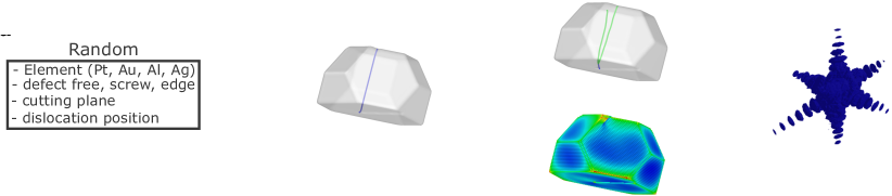
In order to build the dataset required for training the neural network (NN), several material simulation tools were used. The data pipeline allows one to generate simulated CXDPs very close to the ones obtained from Bragg CXD experiments. Fig. 1 illustrates our approach for the creation of 3D CXDPs. The geometry considered in this study is derived from the Wulff construction, i.e., the equilibrium crystal shape of a free-standing crystallite obtained by Gibbs thermodynamic principle, which minimizes the total surface free energy associated to the crystal-medium interface. [37] In order to take into account the presence of a solid-solid interface, i.e. the presence of an underlying substrate as in the experimental nanoparticles, the so-called Winterbottom shape, which can be described as a truncated Wulff construction, is employed.[38]. An example of a simulated crystal is shown in Fig. 1b-d. Only fcc transition metals are considered in this study (Al, Au, Ag, Pt), for which the Wulff/ Winterbottom geometries mostly consist of {1 1 1} and {1 0 0} facets. The Winterbottom constructions are generated using the atomistic simulation code MERLIN [39], by creating a cube of atoms and cutting it along the <1 1 1> and <1 1 0> crystallographic directions, the position of the cut planes being defined by the ratio of the surface energies / and / of the material/potential of interest. The lattice orientations corresponding to the axes of the simulation cell are x[1 0 0], y[0 1 0] and z[0 0 1] and are kept constant for all configurations. The interface plane is selected randomly among the eight possible {1 1 1} planes, and is cut at a random position corresponding to 65% - 75% of the height of a free standing Wulff particle.
Two crystal sizes are considered in this study, the small crystals consist of 40x40x40 unit cells (Supplementary Figure 1) while the large crystals are made up of 80x80x80 unit cells (Supplementary Figure 2). This corresponds to a size of 15x15x(9 -12)nm3 / 100000-140000 atoms for the small configurations, and 30x30x(19-25)nm3 / 800000-950000 atoms for the large configurations, the height and number of atoms in the the crystal depend on the distance of the interface plane with respect to the centre of the particle, and on the lattice parameter of the element considered. For the purpose of this study, we focus on line defects, namely, edge and screw dislocations. A single dislocation and its corresponding displacement field (hypothesis of an isotropic and semi-infinite volume, see Ref. [22]) is introduced following two strategies. In the first type of configurations, hereafter referred as CD, the dislocation is systematically introduced close to the centre, within a range not exceeding 10% of the lateral size of the particle. In the second type of configurations, hereafter referred to as RPD, the position of the dislocation is completely random. The simulated dislocations have a Burgers vector of b = [1 0] which is kept constant for all the configurations. This implies that the initial line directions are t = [1 0] and t = [1 1 ] for the screw and edge dislocations, respectively. If the Burgers vector and line direction of the dislocations are not varied, the random selection of the interface plane ensures that a large variety of orientations of the dislocation line with respect to the normal of the interface plane is available in the dataset as shown in Supplementary Figures 1 & 2.
Once the atomistic configurations are generated, the next step is to obtain accurate and realistic relaxed configurations that reproduce as faithfully as possible the displacement fields measured in the experimental particle. To do so, Molecular Statics simulations are carried out with the open-source Large-scale Atomic/Molecular Massively Parallel Simulator (LAMMPS) [40]. The interaction between atoms are modelled with different embedded-atom model (EAM) potentials that accurately reproduce elastic properties as well as surface and stacking fault energies, parameters that are essential to get an accurate description of the relaxed defects. For Al, Ag, Au and Pt we use the EAM potentials developed by Mishin et al. [41], Williams et al. [42], Grochola et al. [43] and Zhou et al. [44] respectively.
The crystals are relaxed at 0 Kelvin using a conjugate gradient algorithm. If the dislocations introduced close to the centre of the nanocrystals are stabilized by the image forces during relaxation, one notable challenge is the tendency of the dislocations introduced close to a free surfaces to escape the crystal during the energy minimization. In order to prevent this phenomenon, the energy tolerance is used as the main stopping criterion for the energy minimization. The latter is defined as the energy change between two successive iterations divided by the total energy of the system, and is set to a value of for the RPD configurations. This value is sufficiently high to ensure that the dislocations dissociate into Shockley partials and remain in the crystal at the end of the relaxation, as shown in Fig. 1c and Supplementary Figures 1, 2 & 3. The small number of minimization steps also prevents large rotations of the dislocations during the relaxation. It was indeed observed that edge dislocations are prone to rotate (thus becoming a mixed dislocation) during the energy minimization, especially when they are introduced in the vicinity of the free surfaces. Limiting the number of relaxation steps allows to retain the edge and screw character of the dislocation during the relaxation, even if dislocations very close to the free surfaces tend to have a mixed character as illustrated in Supplementary Figures 1, 2 & 3. Each dataset typically contains 1000 relaxed configurations with one third of defect free nanocrystals, one third containing a relaxed screw dislocation and the last third with a relaxed edge dislocation. The time required for the energy minimization of a full dataset ranges between 10 and 25 minutes for the small crystal dataset and 1h30 minutes and 4h for the large crystal dataset.
The last step in the dataset creation is the calculation of the three-dimensional CXDPs that are used as input data for our CNN. This is done by summing the amplitudes scattered by each atom with its phase factor, following a kinematic approximation:
| (1) |
where q is the scattering vector, (q) and are respectively the atomic scattering factor and position of atom j. Note that the crystallographic convention is used in this manuscript, i.e. the 2 factor is not included in , which implies that a given value corresponds to a real space distance of . The computation is performed with a GPU using the PyNX[45] scattering package, which considerably speeds up the calculation of the CXDPs. Given the large number of atoms ( – atoms) and the large number of CXDPs that are generated for each dataset (2000-15000), the calculations are performed on 64x64x64 reciprocal space points. The size of the 3D array is a trade-off between achieving a high-enough resolution in the reciprocal space, which is required for an accurate comparison with the experimental CXDPs and keeping the time required to generate the dataset reasonable. Using a POWER9 machine, each CXDP is calculated in 0.25s for the small configurations and 2s for the large configuration. A dataset containing 10000 CXDPs is therefore typically generated in 40 minutes for the small nanocrystals and 6 hours for the large ones.
In order to introduce enough variation in the dataset and prevent overfitting of the model to the training set (Supplementary Figure 4), each CXDP is rotated randomly around the chosen vector, typically we consider 10 random orientations for each relaxed configuration. The reciprocal space sampling (q) is also varied, which is equivalent to zooming around the Bragg reflection of interest (Supplementary Figure 14). A low reciprocal space resolution (coarse sampling / large q) can have detrimental effects on the accuracy of the network predictions (Supplementary Figure 14c). To prevent this loss in accuracy, we typically selected q values for which the oversampling ratio is consistent with the one used for experimental data. Note that even for the largest q values, the oversampling criteria as defined by Sayre [46] are still fulfilled, as it is always the case for the experimental CXDPs. Since the simulated particles are significantly smaller than the experimental ones (typically by one order of magnitude), this also implies that a larger portion of the Brillouin zone is selected for the simulated particles. We will see in the following that this has little consequence for the accuracy of the network predictions. Before training the NN, the distribution of dislocation positions is typically estimated by comparing the maximum of the intensity scattered by the atomistic configurations in the dataset with the maximum of the intensity scattered by a defect free crystal with a similar number of atoms (Supplementary Figure 15).
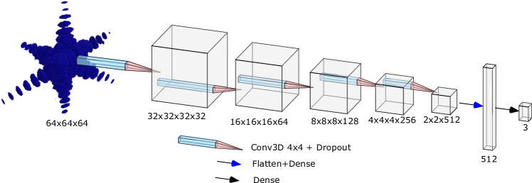
Convolutional neural network
The NN model architecture is displayed in Fig. 2. It takes as input the 646464 image of the CXDP intensity and encodes it through a series of convolution and fully connected layers. Dropout [47] is used in all layers with a dropout rate of 0.2, to avoid overfitting. This is a standard architecture, nevertheless it already gives very accurate predictions on the simulated dataset. Increasing the size of the model, adding extra layers or increasing the number of filters in the convolution layers does not increase the model efficiency and even leads to an overfit of the training dataset in some cases.
Training is performed using Adam optimization[48] with a learning rate of 10-3 and a batch size of 64. A large amount of 3D datasets are simulated. They systematically specify the correct output (defect class) for a given input (3D CXDP intensity), and minimise a categorical cross-entropy loss that quantifies the difference between the predicted and the correct class labels (defect free, screw and edge). Through this minimisation, the weights (i.e., parameters) of the neural network are optimised to reduce the classification error. The weights of each convolutional and fully connected layers are initialized randomly. Moreover, the instances of the training dataset are processed in a random order. Nonetheless, two independent trainings for a given dataset a CNN always gives a very similar probability distribution as illustrated in Supplementary Figure 16. The simulated data are split into training, validation and test sets. The model fit is performed with the training set and stopped when the validation set accuracy reaches a maximum. The final model prediction on the test set containing 11556 CXDPs calculated from 1284 atomistic configurations reaches a very high total accuracy score of 97.2%. In addition, the confusion matrix displayed in Supplementary Figure 7 shows that almost all defect free crystals are predicted. Most of the errors (4.7%) come from edge dislocations predicted as screw. Furthermore, as illustrated in Supplementary Figures 11 & 12, a simpler two classes model (Supplementary Figure 10) predicting either a defect free oe a defective crystal can reach an even higher accuracy. From an occlusion sensitivity test[49] on a simulated CXDP shown in Supplementary Figure 13, we demonstrate that the NN mainly uses the vicinity of the Bragg peak to make its prediction.
Validation on experimental data
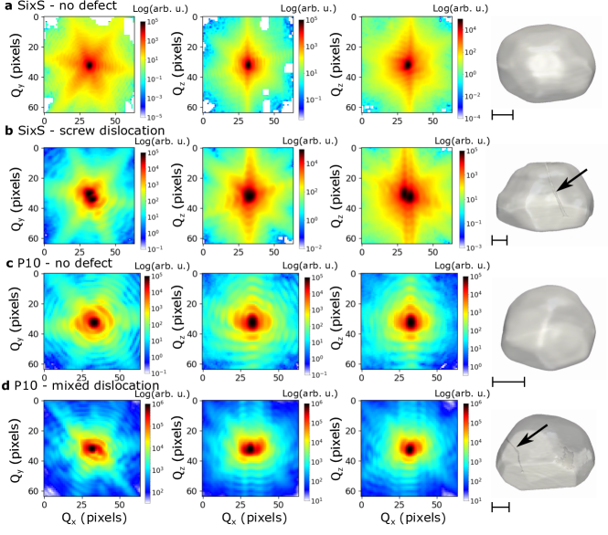
The experimental datasets correspond to 3D reciprocal space maps obtained by measuring the Bragg CXDPs of Pt nanoparticles. Single particles were measured either at the SixS beamline of synchrotron SOLEIL (Orsay, France) or at the P10 beamline of synchrotron PETRA (Hamburg, Germany). The 3D Bragg CXDPs were collected at the asymmetrical Pt Bragg reflection at the SixS beamline or at the symmetrical (specular) 111 Pt Bragg reflection at the P10 beamline. The experimental reciprocal space datatsets have been orthonormalised using the xrayutilities package [50]. Fig. 3 displays the CXDPs of the experimental datasets, as well as their reconstructed Bragg electron density using phase retrieval algorithms. Defect-free (Figs. 3a,c) as well as defective crystals (Figs. 3b,d) were measured. A closer look at Figs. 3(b,d) reveals the variety of dislocation configurations that is found in experimental nanocrystals. These dislocations were most likely nucleated during the growth of the nanoparticles, and did not escape during the annealing at 1100∘C, suggesting that they are strongly pinned in the nanocrystal. For the SixS data, the screw dislocation is close to the center of the nanocrystal (Burgers vector of b = [10]). On the other hand, the dislocation in the P10 defective nanocrystal is closer to the free surfaces. In addition, the dislocation line is not perfectly straight and parallel to the Burgers vectors (b = [101]). It can thus be described as a mixed dislocation with a dominant screw character.
In order to reinforce the agreement between the simulated and experimental datasets each diffraction measurement is preprocessed before computing the model prediction. The CXDP center of mass is placed at the center of the array, as it is also the case for the simulated data. Finally, the CXDP is normalized so that the maximum is equal to 1.
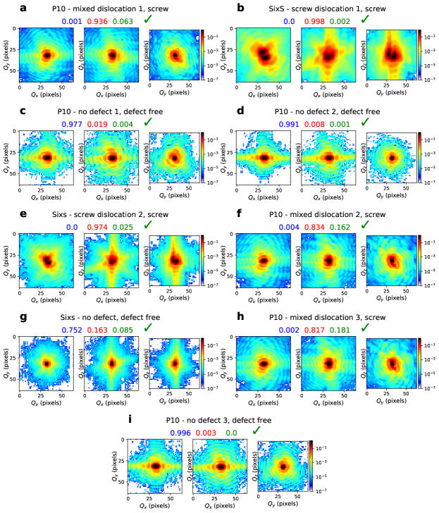
The results of our best NN model on the preprocessed CXDPs are displayed in Fig. 4 along with slices along , and for each experimental CXDP. Some crystals were measured several times under different experimental conditions (temperature, gas environment) for example P10 - no defect 1, 2 and 3 in Fig. 4), allowing us to compare the model predictions for the same crystal but with slightly different CXDPs.
The performances of this model on experimental data are excellent, all the experimental examples being predicted in the correct class and most of them with a very high probability (> 95%). Although still very good, the predictions for the P10 data (mixed dislocation) are generally slightly worse with an accuracy ranging between 82 and 94%. This is not surprising given the mixed type of dislocation (with a dominant screw character), which necessarily increases the probability of identifying the defect as an edge dislocation. Nonetheless, even if the dislocation is located close to a free surface and therefore induces weak distortions in the CXDP (Fig. 3d), our model still manages to identify this crystal as defective with almost a 100% probability. This demonstrates the robustness of the model trained on this dataset, which can predict both centered and off-centered dislocations with a very high accuracy.
The simulated training dataset used to fit the NN model has a large influence on the accuracy of the predictions on experimental data. This dataset must contain enough diversity, while sharing enough similarities with the experimental CXDPs. The predicted probabilities on experimental data for the same model architecture but different simulated training datasets are shown in Table 1. Six different simulated datasets have been trained: (1) single element (Pt) unrelaxed small crystals, 100% centered dislocations (CD), (2) relaxed Pt small crystals (100% CD), (3) relaxed Pt large crystals (100% CD), (4) relaxed large crystals with multiple elements (Au and Pt) (100% CD), (5) relaxed multi-elements large crystals with dislocations at random position (100% RPD) and (6) relaxed multi-elements large crystals with a mix of CD and RPD configurations (75% CD and 25% RPD). The first two rows of Table 1 emphasize the importance of accurately modelling the displacement field of the dislocations. Indeed, while these two models trained on relaxed and unrelaxed datasets predict accurately the defect free configurations, they fail at identifying the mixed dislocation (P10 data). However, the model trained on the relaxed dataset performs much better on the SixS-"screw" data, which is correctly identified as a screw dislocation (see also Supplementary Figure 9). On the other hand, the size of the relaxed crystals does not have a major impact on the accuracy of the model (Table 1, second and third row), although the predictions of the models trained on the large configurations is slightly more accurate, in particular for defect free configurations (Supplementary Tables 2 and 6).
The addition of several elements in the dataset improves the accuracy of the predictions for the SixS data, but has no effect on the P10 data (Table 1, fourth row). Nonetheless, mixing several elements in the dataset generally results in better model predictions compared to the models based on single elements, in particular for the large crystal size (Supplementary Tables 5-8). The position of the dislocation also has a major impact on the model predictions. As seen from Table 1 (sixth row), introducing the dislocation at random positions, including positions close to the crystal free surfaces, results in more accurate predictions for the P10 data. However, this improvement is at the expense of the predictions for the SixS data, which is correctly identified as a dislocation, but with an edge character instead of a screw. The predictions for the defect free data are not affected and still excellent (see also Supplementary Figure 8).
In order to obtain accurate predictions simultaneously for both P10-"mixed" and SixS-"screw" dislocations, one must increase the diversity in the training dataset. This has been achieved by building a dataset consisting of a mix of CD and RPD configurations (Table 1, seventh row). Training the CNN on this mixed dataset significantly enhances the performances of the model and allows to predict correctly and with a very high accuracy all the experimental examples.
We must emphasize that, despite the differences in the ability of the models to generalize to experimental data, the accuracy on the simulated test data for each training dataset is always higher than 86% (Supplementary Tables 1 & 5). Our work illustrates the necessity of using a simulated trained datasets close to real structures: atomistically relaxed nanoparticles with an accurate modelling of the dislocation displacement field, multiple atomic elements and random location of the dislocations. It also demonstrates that a convolutional neural network can predict dislocations in a crystal from its 3D coherent diffraction pattern. Combined with the fast scanning capabilities of some synchrotron beamlines [51], this approach could be used to perform a fast screening of the nanocrystals on a sample of interest. This would allow to determine the proportion of defect free nanocrystals as well as nanocrystals containing a specific type of crystal defect, and select the best candidate for a coherent diffraction imaging experiment. In addition, if the CNN was only tested on metallic fcc particles, we foresee that it could be extended to more complex systems like for instance multi-element particles.
From 3D coherent X-ray CXDPs, we used a convolutional neural network to predict defect classes. As a result, we obtain an automatic procedure for defect classification in fcc metals, which does not require any user-manipulation, any intensive live data mining, and achieves high-accuracy classification even in the presence of defects close to the free surfaces of the nanocrystals. This tool can be exploited during experiment execution to provide rapid feedback to the investigator, enables one to identify on the fly target defect types present in individual nanocrystals, and furthers the possibility of unsupervised data collection, extremely relevant given the increases data rates expected at ever improving facilities. Our study paves the way for defect recognition of three-dimensional structural data in big-data materials science.
Methods
Training the network
We used the python deep-learning API Keras [52] running the TensorFlow backend [53] to build, develop and train our NN. The training was performed in parallel on two NVIDIA Tesla V100 GPUs and a POWER9 computer. We use a categorical cross-entropy loss function where is the batch size, the number of classes, for data element if the true class is and otherwise. is the predicted probability for class . The simulated dataset is divided into training, validation and test, corresponding respectively to 85%, 10% and 5% of the total dataset. The model is trained with a learning rate of and a batch size of 64 on the training set until the model accuracy calculated on the validation set reaches a plateau (Supplementary Figures 5, 6 & 11). A typical training requires between 15 and 30 minutes depending on the dataset (8-10 seconds per epoch and 100-200 epochs). Decreasing the learning-rate and increasing the batch size does not further improve the model accuracy. Once trained, the model performance is evaluated on the test set and reaches a total accuracy >86% on the simulated data for all models presented in Table 1.
Sample growth
Pt nanocrystals were prepared by the solid-state dewetting of a 30-nm thin Pt film for 24 hours at 1100∘C in air[54]. The Pt film was deposited on -Al2O3 (sapphire) with an electron beam evaporator. The Pt nanocrystals have their c-axis oriented along the [111] direction normal to the (0001) sapphire substrate. A standard photolithography method was employed to prepare a patterned layer of photoresist on sapphire prior to the electron beam evaporation of Pt. The lithographic processing route ensured that a number of dewetted Pt particles are well-separated from their neighbors and that only one crystallite is irradiated by the incoming x-ray beam. The particle size ranges from 100 nm to 700 nm.
Data availability
The data supporting the findings of this work are available from the corresponding author on reasonable request.
Acknowledgements
We acknowledge financial support from the European Research Council (ERC) under the European Union’s Horizon 2020 research and innovation programme (grant agreement No. 818823). We also thank the support by a grant from the Ministry of Science & Technology, Israel and CNRS, France.
Competing interest
The authors declare no competing interests.
Author contributions statement
B.L. and M.D. performed the atomistic simulations. E.B. developed the convolutional neural network. M.-I.R. processed the experimental data. E.R. and E.A. prepared the samples. M.D., M.-I.R, S.L, A.R., A.C. performed the experiments at the SixS beamline of synchrotron SOLEIL (experiment number: 20181680) and M.D., M.-I.R, S.L and M.S. performed the experiments at the P10 beamline of synchrotron PETRA (experiment number: I-20180962). B.L., E.B., M.D. and M.-I.R. wrote the manuscript and all authors reviewed the manuscript. B.L., E.B. and M.D. contributed equally to this work and are considered "co-first author" of this manuscript.
Additional information
Supplementary Information is available for this paper at XX.
References
- [1] Wang, H., Jang, Y.-I., Huang, B., Sadoway, D. R. & Chiang, Y.-M. TEM study of electrochemical cycling-induced damage and disorder in LiCoO2 cathodes for rechargeable lithium batteries. \JournalTitleJournal of The Electrochemical Society 146, 473–480 (1999).
- [2] Bei, H., Shim, S., Pharr, G. & George, E. Effects of pre-strain on the compressive stress–strain response of Mo-alloy single-crystal micropillars. \JournalTitleActa Mater. 56, 4762–4770 (2008).
- [3] Ohno, Y. et al. Optical properties of dislocations in wurtzite ZnO single crystals introduced at elevated temperatures. \JournalTitleJournal of Applied Physics 104, 073515 (2008).
- [4] Bittner, F., Freudenberger, J., Schultz, L. & Woodcock, T. The impact of dislocations on coercivity in L10-MnAl. \JournalTitleJournal of Alloys and Compounds 704, 528–536 (2017).
- [5] Shin, N., Chi, M., Howe, J. Y. & Filler, M. A. Rational Defect Introduction in Silicon Nanowires. \JournalTitleNano Letters 13, 1928–1933 (2013).
- [6] Ulvestad, A. et al. Topological defect dynamics in operando battery nanoparticles. \JournalTitleScience 348, 1344–1347 (2015).
- [7] Attariani, H., Momeni, K. & Adkins, K. Defect Engineering: A Path toward Exceeding Perfection. \JournalTitleACS Omega 2, 663–669 (2017).
- [8] Behrens, M. et al. The active site of methanol synthesis over Cu/ZnO/Al2O3 industrial catalysts. \JournalTitleScience 336, 893–897 (2012).
- [9] Vendelbo, S. B. et al. Visualization of oscillatory behaviour of Pt nanoparticles catalysing CO oxidation. \JournalTitleNature Materials 13, 884–890 (2014).
- [10] Carter, C. B. & Williams, D. B. Transmission Electron Microscopy: A Textbook for Materials Science. Diffraction. II (Springer Science & Business Media, 1996).
- [11] Livet, F. Diffraction with a coherent X-ray beam: dynamics and imaging. \JournalTitleActa Crystallographica Sect. A 63, 87–107 (2007).
- [12] Sutton, M. A review of X-ray intensity fluctuation spectroscopy. \JournalTitleComptes Rendus Phys. 9, 657–667 (2008).
- [13] Beutier, G. et al. Strain inhomogeneity in copper islands probed by coherent x-ray diffraction. \JournalTitleThin Solid Films 530, 120–124 (2013).
- [14] Favre-Nicolin, V. et al. Analysis of strain and stacking faults in single nanowires using bragg coherent diffraction imaging. \JournalTitleNew Journal of Physics 12, 035013 (2010).
- [15] Jacques, V. L. R. et al. Bulk dislocation core dissociation probed by coherent x-rays in silicon. \JournalTitlePhysical Review Letters 106, 065502 (2011).
- [16] Fienup, J. R. Phase retrieval algorithms: a comparison. \JournalTitleAppl. Opt. 21, 2758–2769 (1982).
- [17] Marchesini, S. et al. X-ray image reconstruction from a diffraction pattern alone. \JournalTitlePhysical Review B 68, 140101 (2003).
- [18] Robinson, I. & Harder, R. Coherent x-ray diffraction imaging of strain at the nanoscale. \JournalTitleNature Materials 8, 291–298 (2009).
- [19] Dupraz, M. et al. 3D imaging of a dislocation loop at the onset of plasticity in an indented nanocrystal. \JournalTitleNano Letters 17, 6696–6701 (2017).
- [20] Clark, J. N. et al. Three-dimensional imaging of dislocation propagation during crystal growth and dissolution. \JournalTitleNature Materials 14, 780–784 (2015).
- [21] Hofmann, F. et al. Nanoscale imaging of the full strain tensor of specific dislocations extracted from a bulk sample. \JournalTitlePhys. Rev. Materials 4, 013801 (2020).
- [22] Dupraz, M., Beutier, G., Rodney, D., Mordehai, D. & Verdier, M. Signature of dislocations and stacking faults of face-centred cubic nanocrystals in coherent x-ray diffraction patterns: a numerical study. \JournalTitleJournal of applied crystallogr. 48, 621–644 (2015).
- [23] Krueger, S. et al. Fault detection and feature analysis in interferometric fringe patterns by the application of wavelet filters in convolution processors. \JournalTitleJournal of Electronic Imaging 10, 228–233 (2001).
- [24] Caulier, Y., Spinnler, K. P., Wittenberg, T. M. & Bourennane, S. Specific features for the analysis of fringe images. \JournalTitleOptical Engineering 47, 057201 (2008).
- [25] Jueptner, W. P. O., Kreis, T. M., Mieth, U. & Osten, W. Application of neural networks and knowledge-based systems for automatic identification of fault-indicating fringe patterns. In Interferometry ’94: Photomechanics, vol. 2342, 16–26 (International Society for Optics and Photonics, 1994).
- [26] Nash, W., Drummond, T. & Birbilis, N. A review of deep learning in the study of materials degradation. \JournalTitlenpj Materials Degradation 2, 37 (2018).
- [27] Tabernik, D., Šela, S., Skvarč, J. & Skočaj, D. Segmentation-based deep-learning approach for surface-defect detection. \JournalTitleJournal of Intelligent Manufacturing 31, 759–776, DOI: 10.1007/s10845-019-01476-x (2020).
- [28] Ye, R., Pan, C.-S., Chang, M. & Yu, Q. Intelligent defect classification system based on deep learning. \JournalTitleAdvances in Mechanical Engineering 10, 1687814018766682 (2018).
- [29] Roberts, G. et al. Deep learning for semantic segmentation of defects in advanced stem images of steels. \JournalTitleScientific Rep. 9, 12744 (2019).
- [30] Denning, P. J. & Lewis, T. G. Exponential laws of computing growth. \JournalTitleCommunications of the ACM 60, 54–65 (2016).
- [31] Ziletti, A., Kumar, D., Scheffler, M. & Ghiringhelli, L. M. Insightful classification of crystal structures using deep learning. \JournalTitleNature comm. 9, 2775 (2018).
- [32] Cherukara, M. J., Nashed, Y. S. G. & Harder, R. J. Real-time coherent diffraction inversion using deep generative networks. \JournalTitleScientific Rep. 8, 16520 (2018).
- [33] Chan, H. et al. Real-time 3d nanoscale coherent imaging via physics-aware deep learning. Preprint at https://arxiv.org/abs/2006.09441 (2020).
- [34] Wu, L., Juhas, P., Yoo, S. & Robinson, I. Complex imaging of phase domains by deep neural networks. \JournalTitleIUCrJ 8, 12–21 (2021).
- [35] Scheinker, A. & Pokharel, R. Adaptive 3D convolutional neural network-based reconstruction method for 3d coherent diffraction imaging. \JournalTitleJournal of Applied Physics 128, 184901 (2020).
- [36] Wu, L. et al. 3D coherent x-ray imaging via deep convolutional neural networks. Preprint at http://arxiv.org/abs/2103.00001 (2021).
- [37] Miracle-Sole, S. Wulff shape of equilibrium crystals. Preprint at https://arxiv.org/abs/1307.5180 (2013).
- [38] Winterbottom, W. Equilibrium shape of a small particle in contact with a foreign substrate. \JournalTitleActa Metallurgica 15, 303–310 (1967).
- [39] Rodney, D. Merlin in a nutshell. Unpublished (2010).
- [40] Plimpton, S. Fast parallel algorithms for short-range molecular dynamics. \JournalTitleJ Comp Phys 117, 1–19 (1995).
- [41] Mishin, Y., Farkas, D., Mehl, M. J. & Papaconstantopoulos, D. A. Interatomic potentials for monoatomic metals from experimental data andab initiocalculations. \JournalTitlePhysical Review B 59, 3393–3407 (1999).
- [42] Williams, P. L., Mishin, Y. & Hamilton, J. C. An embedded-atom potential for the Cu–Ag system. \JournalTitleModelling and Simulation in Materials Science and Engineering 14, 817–833 (2006).
- [43] Grochola, G., Russo, S. P. & Snook, I. K. On fitting a gold embedded atom method potential using the force matching method. \JournalTitleThe Journal of Chemical Physics 123, 204719 (2005).
- [44] Zhou, X. W., Johnson, R. A. & Wadley, H. N. G. Misfit-energy-increasing dislocations in vapor-deposited CoFe/NiFe multilayers. \JournalTitlePhys. Rev. B 69, 144113 (2004).
- [45] Favre-Nicolin, V., Coraux, J., Richard, M.-I. & Renevier, H. Fast computation of scattering maps of nanostructures using graphical processing units. \JournalTitleJournal of Applied Crystallography 44, 635–640 (2011).
- [46] Sayre, D. Some implications of a theorem due to shannon. \JournalTitleActa Crystallographica 5, 843–843 (1952).
- [47] Srivastava, N., Hinton, G. E., Krizhevsky, A., Sutskever, I. & Salakhutdinov, R. Dropout: a simple way to prevent neural networks from overfitting. \JournalTitleJ. Mach. Learn. Res. 15, 1929–1958 (2014).
- [48] Kingma, D. P. & Ba, J. Adam: A method for stochastic optimization. Preprint at https://arxiv.org/abs/1412.6980 (2017).
- [49] Zeiler, M. D. & Fergus, R. Visualizing and understanding convolutional networks. In Fleet, D., Pajdla, T., Schiele, B. & Tuytelaars, T. (eds.) Computer Vision – ECCV 2014, 818–833 (Springer International Publishing, Cham, 2014).
- [50] Kriegner, D., Wintersberger, E. & Stangl, J. xrayutilities : a versatile tool for reciprocal space conversion of scattering data recorded with linear and area detectors. \JournalTitleJournal of Applied Crystallography 46, 1162–1170 (2013).
- [51] Chahine, G. A. et al. Imaging of strain and lattice orientation by quick scanning X-ray microscopy combined with three-dimensional reciprocal space mapping. \JournalTitleJournal of Applied Crystallography 47, 762–769 (2014).
- [52] Chollet, F. et al. Keras. https://github.com/fchollet/keras (2015).
- [53] Abadi, M. et al. TensorFlow: Large-scale machine learning on heterogeneous systems (2015). Software available from tensorflow.org.
- [54] Li, N. et al. Continuous scanning for Bragg coherent X-ray imaging. \JournalTitleScientific Rep. 10, 12760 (2020).
Figures and Tables
| P10 mixed 1 | SixS Screw 1 | P10 no defect 1 | P10 no defect 2 | SixS Screw 2 | P10 mixed 2 | SixS no defect | P10 mixed 3 | P10 no defect 3 | |
|---|---|---|---|---|---|---|---|---|---|
| Pt unrelaxed small crystals CD | p 99 s 1 e 0 | p 0 s 3 e 97 | p 100 s 0 e 0 | p 100 s 0 e 0 | p 0 s 1 e 99 | p 97 s 2 e 1 | p 100 s 0 e 0 | p 100 s 0 e 0 | p 100 s 0 e 0 |
| Pt relaxed small crystals CD | p 99 s 1 e 0 | p 0 s 100 e 0 | p 100 s 0 e 0 | p 100 s 0 e 0 | p 0 s 69 e 31 | p 72 s 18 e 10 | p 72 s 16 e 12 | p 92 s 6 e 2 | p 100 s 0 e 0 |
| Pt relaxed big crystals CD | p 99 s 0 e 1 | p 0 s 100 e 0 | p 100 s 0 e 0 | p 100 s 0 e 0 | p 25 s 38 e 37 | p 99 s 0 e 1 | p 99 s 0 e 1 | p 99 s 0 e 1 | p 100 s 0 e 0 |
| Multi-elements relaxed big crystals CD | p 98 s 0 e 2 | p 0 s 100 e 0 | p 100 s 0 e 0 | p 100 s 0 e 0 | p 0 s 98 e 2 | p 88 s 5 e 8 | p 99 s 0 e 1 | p 94 s 2 e 3 | p 100 s 0 e 0 |
| Multi-elements relaxed big crystals RPD | p 9 s 53 e 38 | p 0 s 36 e 64 | p 100 s 0 e 0 | p 100 s 0 e 0 | p 0 s 8 e 92 | p 0 s 58 e 42 | p 99 s 1 e 0 | p 0 s 63 e 37 | p 100 s 0 e 0 |
| Multi-elements relaxed big crystals 75% CD, 25% RPD | p 0 s 94 e 6 | p 0 s 100 e 0 | p 98 s 2 e 0 | p 99 s 1 e 0 | p 0 s 97 e 3 | p 0 s 84 e 16 | p 75 s 16 e 9 | p 0 s 82 e 18 | p 100 s 0 e 0 |