Leakage Current Simulations of Low Gain Avalanche Diode with Improved Radiation Damage Modeling
Abstract
We report precise TCAD simulations of IHEP-IME-v1 Low Gain Avalanche Diode (LGAD) calibrated by secondary ion mass spectroscopy (SIMS). Our setup allows us to evaluate the leakage current, capacitance, and breakdown voltage of LGAD, which agree with measurements’ results before irradiation. And we propose an improved LGAD Radiation Damage Model (LRDM) which combines local acceptor removal with global deep energy levels. The LRDM is applied to the IHEP-IME-v1 LGAD and able to predict the leakage current well at -30 ∘C after an irradiation fluence of . The charge collection efficiency (CCE) is under development.
keywords:
LGAD , TCAD simulation , acceptor removal , neutron irradiation , radiation model1 Introduction
Low Gain Avalanche Diodes (LGADs) are characterized by an excellent timing performance with a time resolution of at least 50 ps and have been developed extensively in the past few years [1, 2, 3, 4, 5, 6, 7, 8], especially by the CERN RD50 Collaboration [9] in view of the High Luminosity Large Hadron Collider (HL-LHC) upgrade at CERN.
LGADs will be used in ATLAS and CMS experiments at the LHC. In particular, they will be used place in the High Granularity Timing Detector (HGTD) [10] of ATLAs and in the End-cap Timing Layer (ETL) [11] of CMS. Radiation hardness up to is required by ATLAS and represents the main challenge in the development of LGAD sensors. Technology Computer-Aided Design (TCAD) is usually employed in the optimization of semiconductor processing and for predicting device performance. In particular, TCAD is useful to accurately predict LGAD sensor features before and after irradiation and, in turn, to understand the mechanisms behind radiation damage in LGADs.
A major goal in the design of LGAD sensors is to control the breakdown voltage () at an appropriate level due to the high electric field near the gain layer that easily exceeds the threshold from linear-model to geiger-model. A longer range of operating voltage with higher could obtain an appropriate gain, meanwhile ensuring carrier velocity saturation when the device works. In this framework, numerical simulations based on TCAD tools are useful in assessing the performance of calibrated devices before manufacturing, in turn, tuning the sought-after breakdown voltage.
Previously TCAD analysis of of LGAD sensors [12, 13] have shown that strongly depends on the gain layer doping profile and the avalanche model. Calibrated process simulation with SIMS measurement may be used to minimize the influence of doping uncertainty, whereas using appropriate physical models allows one to predict the threshold of breakdown more precisely. In this paper, we report results obtained by TCAD simulations of the full process of IHEP-IME-v1 LGADs. The good agreement between TCAD simulations and experimental measurements confirms that this kind of analysis will be a resource to optimize the LGAD performance in the next production stage. It also paves the way for establishing the solid ground for simulations of irradiation processes.
Furthermore, including previous phenomenological studies to build a better model for irradiated LGAD sensors and improve predictions of TCAD simulations is an important topic in itself [9]. In previous studies [14, 15], different models have been applied to TCAD simulations to obtain qualitative results for the behavior of irradiated LGAD sensors. The results from a comprehensive study [16] analyzing the gain factor has been verified on irradiated LGAD sensors from different vendors. The leakage current and capacitance of irradiated LGAD sensor obtained in [17, 18, 19] show good agreement with simulated results at room temperature (T=27). In this paper, the details and performance of IHEP-IME-v1 LGAD sensors are introduced in Sec. 2. Then we present the results of precise TCAD simulations based on IHEP-IME-v1 LGAD sensors in Sec. 3, and introduce a TCAD-LRDM model to evaluate the leakage current and the capacitance of irradiated LGAD sensors at low temperature (T=-30) in Sec. 4. The leakage current obtained from simulations are in good agreement with experimental measurements, indicating the validity of our model, which combines the acceptor removal with the deep energy levels.
2 Devices under study
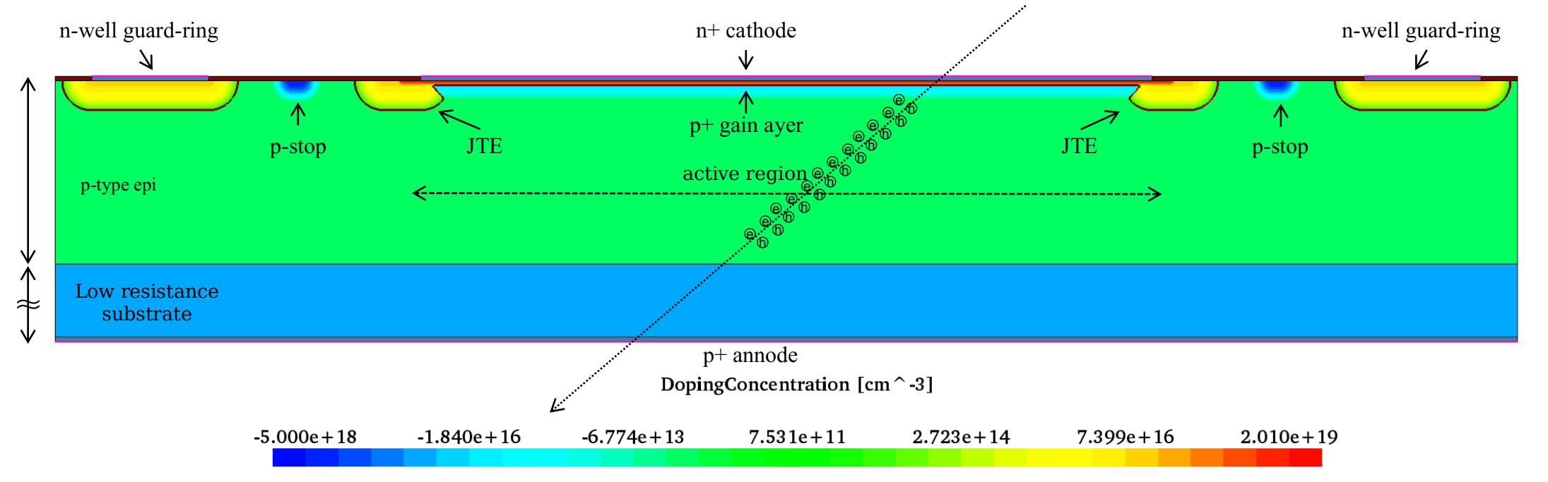
The IHEP-IME-v1 LGAD sensor is being developed by the Institute of High Energy Physics and the Institute of Microelectronics of the Chinese Academy of Sciences [20]. A cross-section of IHEP-IME-v1 LGAD structure is shown in Fig.1. Typically,the structure contains a (n++)-(p+)-p-(p++) stack, a junction termination extension (JTE), a p-stop and a guard-ring. JTE is included to possibly prevent premature breakdown [2]. Guard-ring may be regarded as a “cathode” for the peripheral region, and it simultaneously reshapes electric field distribution near the region of JTE. P-stop blocks up the potential connection between cathode and guard-ring, due to JTE diffusion process and interface charges after radiation when the same voltage is applied to cathode/guard-ring. It is manufactured on a 50 high resistivity p-type epi-wafer with 725 supporting substrate. The detailed wafer information is reported in Table 1. The electric field peak in the p+ gain layer is larger than 300 kV/cm when the LGAD sensor operates at nominal bias voltage. In this condition, the drift electrons (a few holes) acquire sufficient energy to generate electron-hole pairs by impact ionization. However, they are still lower than the avalanche threshold. The gain of the LGAD sensor is kept under control at around 10-60, since in this condition good time resolution and signal to noise ratio may be achieved simultaneously, thanks to the carriers multiplication and the thin active region [21].
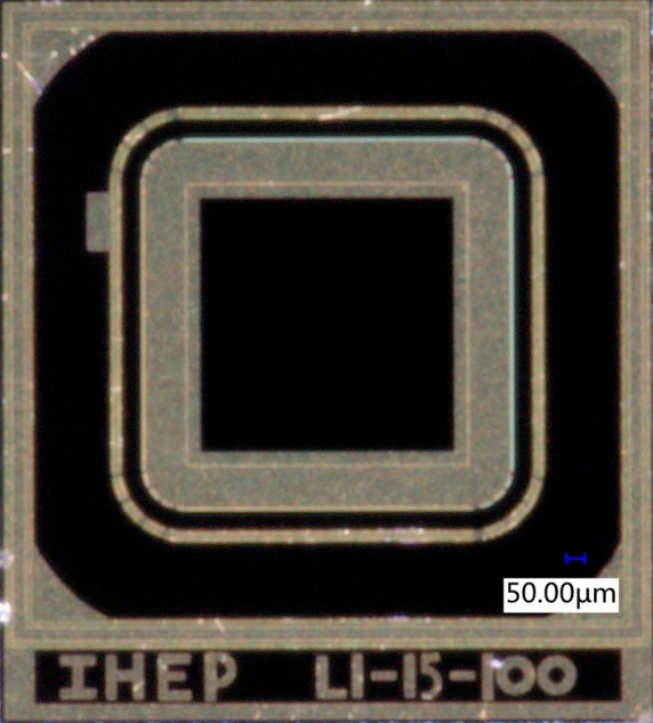
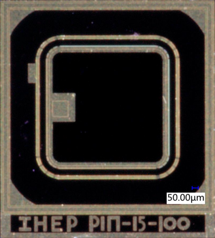
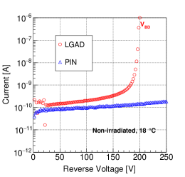
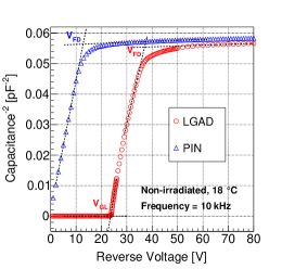
To understand the difference between measurements and simulations, we select two fabricated devices from the IHEP-IME-v1 production line: LGAD (L1-15-100) and PIN (PIN-15-100). They have the same geometry and fabricating process except from the fact that the PIN has no gain layer (see Fig.2 and 2). The active area of both is . Fig.3 and 3 show the I-V and 1/C2-V characteristic curves of LGAD/PIN, measured at room temperature. Owing to the presence of an internal gain, the leakage current of the LGAD sensor can be as high as 15 times the leakage current of PIN. The of LGAD (196 V), defined as the voltage corresponding to a leakage current exceeding , is smaller than PIN diode which does not show breakdown up to 700V. The change in capacitance between gain layer depletion voltage () and full depleted voltage () in LGAD sensor corresponds to the presence of the (n++)-(p+)-p-(p++) stack.
| parameter | value | |
| Epitaxy | thickness | |
| uniformity∗ | 6% | |
| dopant | Boron | |
| resistivity | ||
| Substrate | material | CZ silicon |
| thickness | ||
| orientation | 100 | |
| dopant | Boron | |
| resistivity |
-
1.
∗ Thickness uniformity measured by 9 points.
The effective doping concentration can be obained from as [22]
| (1) |
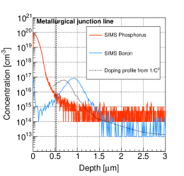
where is the electron charge, is the dielectric constant of silicon and is the area of the active region. The effective doping of the bulk region () is obtained from the slope of 1/C2-V curve before full depletion of the PIN. The corresponding resistivity is consistent with the resistivity of the epitaxial layer provided by the wafer foundry in Table 1. It should be emphasized that equation (1) is accurate if the depleted region grows from the main junction side, a situation usually referred to as the “one-sided junction” approximation. The same method may be applied to LGAD, but the less accurate determination of doping profile such as shifting of depth is obtained(see Fig.4).
3 TCAD simulation
The full TCAD simulation includes device construction and the simulation of its electrical properties. The device construction involves the definition of geometry and doping profile. The geometry may be scaled-down to reduce the time burden and the doping profile may be extracted from SIMS or generated by process simulation. For the simulation of the electrical properties, the selected physical models should consider the influence of high electric field and doping concentration level in LGAD. More details of physical models are in Sec. 3.3.
3.1 Doping profile from SIMS
Fig.4 shows the phosphorus and boron concentrations measured by SIMS. The maximum electric field value appears on the metallurgical junction line. The low energy and extremely high dose of implanted phosphorus lead to a sharp and shallow Ohmic contact made by a n+ layer. The deep p+ gain layer is built by high energy boron implanting where the peak concentration is about . To avoid damages to the wafer surface during the fabrication process of IHEP-IME-v1 LGADs, which is due to the high energy of ions, a thermal screen oxide layer () covers the wafer surface before boron implantation. The influence of this screen oxide layer on the doping profile is discussed in the next section.
3.2 Full process calibration by SIMS
The simulation process needs to be calibrated by SIMS data before being able to provide a prediction of electrical features. The TCAD environment provides a calibrated database referred to as “Advanced Calibration” [23], but there are large discrepancies between simulation based on this database and SIMS data (see Fig.5 and 5). For phosphorus, the simulated doping is shallower than that obtained from SIMS. For boron, there is an additional bump in the tail region, indicating that the channeling effects are overestimated in the simulations. The possible reason for this behavior may be found in the channeling effects of the screen oxide layer mentioned in the last section. Although we use the full process simulation and implant the boron/phosphorus after growing the screen oxide layer, the effects are not suppressed. In order to calibrate the ion implantation step in our simulations, the ratio between the amorphous and channeling doses [23] should be corrected to match our working conditions.
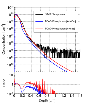
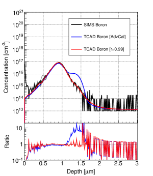
For a data-driven calibration, the ratio of “channeling effects suppression” are adjusted for both phosphorus and boron to minimize . The optimal values are and . After calibration, the simulated doping profiles are closer with SIMS data than default.
3.3 The physical model used in TCAD
The doping dependence, high field saturation on mobility, and temperature dependence on Shockley–Read–Hall Recombination (SRH) are considered, because the effective doping is larger than , the electric field in the gain layer is about and device works in a low-temperature condition. The avalanche is described by a van Overstraeten – de Man model [24] with “parallel” driving force and a bandgap dependence. In the van Overstraeten – de Man model, there are two different sets of parameters to describe the carrier generation coefficient that determines the breakdown threshold of LGAD sensor, depending on whether the electric field is in the range from to or it is larger.
3.4 Simulations of the I-V & C-V characteristics of non-irradiated LGAD sensors
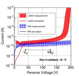
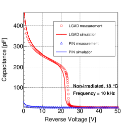
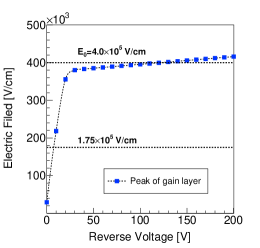
We use PINs and LGADs in order to verify our device simulation setup, and assess the calibrated process simulation as well as the physical model. Several devices are subject to measurement to estimate the intrinsic spread of the I-V characteristics due to the fabrication process and the measurement conditions (denoted by a colored band in Fig.6). The simulated current agrees well with measurements. In particular, simulations reliably predict the breakdown voltage of LGAD sensors. The bias region from to , denoted by the arrow in Fig.6, is the operation region with moderate gain. is the voltage when the maximum electric field at the metallurgical junction line reaches . The predicted breakdown voltage agrees with the prediction from the van Overstraeten model. In Fig.7, we show the electric field peak at the metallurgical junction line (, see Figure 4), which is simulated by TCAD using the calibrated process described in Section 3.2. When the electric field exceeds the threshold , leakage current increases sharply due to the generation of a higher field. The simulated capacitances are shown in Fig.6, and are in good agreement with the measured values. The depleted capacitances of simulation and measurement at 50 V both are 5 pF which is compatible with device geometry.
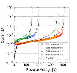
We compare four different sets of simulated and measured I-V characteristics of LGAD sensors after calibration (Fig.8) to verify the reliability of the process simulation setup, which is applied to all sets. The process sets are listed in Table 2. The LGAD sensor considered in Section 2 belongs to set3 with a high implantation energy of phosphorus and high implantation dose of boron. All simulated breakdown voltages show good consistency with measurements. It proves that the calibrated configurations in the process simulation are reliable and could be reproduced by using the appropriate physical models.
| Low Energy (1.00) | High Energy (1.25) | |
|---|---|---|
| Low Dose (1.00) | set2 | set1 |
| High Dose (1.14) | set4 | set3 |
4 Radiation model
4.1 LGAD Radiation Damage Model (LRDM)
Our LRDM TCAD model combines local acceptor removal with global deep energy levels (the Hamburg Penta Trap Model - HPTM [25]) in TCAD simulation to predict the current and capacitance of irradiated LGAD sensors. The acceptor removal takes effect in the gain layer whereas the deep energy levels are implemented in the high resistivity bulk region.
The Poisson equation, which describes the acceptor removal and deep energy levels in the different regions is given by
| (2) |
where is the trap concentration, for donor (acceptor) type of trap and is the trap occupancy for trap i.
In the acceptor removal model, the effective doping after irradiation is given by [26]:
| (3) |
where is equivalent to 1 MeV neutron fluence by NIEL hypothesis, and and are the initial and the effective doping without irradiation, respectively. We set the removal constant to by best-fitting and [22].
Concerning the deep energy levels at low temperature, we assume the validity of the HPTM, since it gives a consistent description of a large set of measurements in PIN with protons fluence range from to . The 5 deep energy levels of HPTM are implemented in silicon material with uniform distribution in TCAD simulations.
In order to achieve the best fitting results, the introduction rate of trap level () for HPTM is set to 0.6050 (default is 0.4335 ) in our simulations.
4.2 Simulated I-V and C-V characteristics of irradiated LGAD sensors
Once we have confirmed our simulation setup and implemented the LRDM, Eq.(2) and the current continuity equations may be solved and the leakage current and capacitance of irradiated LGAD sensors may be estimated. The studied LGAD sensor has been irradiated at the Jozef Stefan Institute (JSI) with a flux of . The measurements are performed at -30 after 60 for 80 minutes annealing.
The leakage current is determined by the residual gain and the deep energy traps as follows [27]:
| (4) |
where is dominated by the acceptor removal and by the deep energy levels. The simulated currents by HPTM and LRDM for are shown in Fig.9. Simulation by LRDM predicts a large increase of the leakage current and in irradiated LGAD sensors, which is consistent with measurements. The discrepancies between simulations and measurements are due to the uncertainty in the irradiation fluence and to temperature fluctuations.
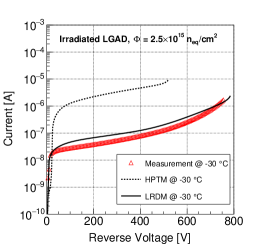
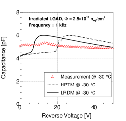
Fig.9 illustrates the LRDM could reproduce the capacitance of irradiated LGAD to a certain degree compared with HPTM. The 1 kHz frequency is applied both in simulation and measurement after irradiation. When the fluence up to , the gain layer is almost disappeared. Under this condition, the device is like a PIN, so the capacitance drops from 400 pF to 6 pF. The behavior of capacitance at low temperature has been reported in previous works for irradiated CNM LGAD sensors [28]. Comparing the extensive measurements [22, 29] for irradiated LGAD sensors at room temperature and low temperature, the capacitance near has a “bump” only at low temperature. The estimated “bump” position voltages are 12.5 V by LRDM, 26.0 V by HPTM and 13.0 V by measurement, where the simulated results by LRDM agree with measurement. However, the theoretical interpretation about the appearance of “bump” is not complete, and the possible cause of the behavior of capacitance at low temperature is related to the complex space charge distribution (such as multi-junction) in irradiated LGAD, which is under investigation.
5 Summary
In this paper, we have presented and verified a full process simulation, including calibration, for the production of IHEP-IME LGAD sensors. Channeling suppression effects have been considered in process simulation using SIMS data and results are in agreement with experiments. We obtain highly consistent characteristics for non-irradiated LGAD sensors, which indicates that our TCAD simulation setup may be reliably employed in the optimization of IHEP-IME-v2 production. It also provides solid ground for simulations of irradiated LGAD sensors.
We have put forward an LRDM TCAD model, which combines local acceptor removal and global deep energy levels, to simulate the characteristics of irradiated LGAD sensors. The simulated leakage current well agrees with experimental results. The LRDM could qualitatively describe the behavior of capacitance at low temperature but need further investigation about capacitance levels.
Our results also pave the way for further studies about the radiation model and the theoretical description of the capacitance in irradiated LGAD sensors. However, present LRDM is still under development and it could not simulate the charge collection efficiency. And those studies will need more measurements supported by other techniques, e.g. deep energy levels in irradiated LGAD may be extracted by Thermally Stimulated Current (TSC) [30] and the electric field distribution may be obtained by edge -Transit Current Technique (e-TCT) [31] or Two-Photon Absorption - Transient Current Technique (TPA-TCT) [32].
Acknowledgment
This work has been supported by the National Natural Science Foundation of China (No. 11961141014), the Scientific Instrument Developing Project of the Chinese Academy of Sciences - Grant (No. ZDKYYQ20200007), and the National Key Research & Development Program (No. 2016YFA0201903). We acknowledge key suggestions from the ATLAS HGTD Collaboration and CERN RD50 Collaboration and thank Joern Schwandt for his comments about the radiation model in TCAD simulations.
References
- [1] G. Pellegrini et al. Technology developments and first measurements of Low Gain Avalanche Detectors (LGAD) for high energy physics applications. Nucl. Instrum. Methods A, 765, 2014. doi: 10.1016/j.nima.2014.06.008.
- [2] H. F. W. Sadrozinski et al. 4D tracking with ultra-fast silicon detectors. Rep. Prog. Phys., 81(2), 2018. doi: 10.1088/1361-6633/aa94d3.
- [3] V. Sola et al. First FBK production of 50 um ultra-fast silicon detectors. Nucl. Instrum. Methods A, 924, 2019. doi: 10.1016/j.nima.2018.07.060.
- [4] Y.Y. Fan et al. Radiation hardness of the low gain avalanche diodes developed by NDL and IHEP in China. Nucl. Instrum. Methods A, 984, 2020. doi:10.1016/j.nima.2020.164608.
- [5] S. Xiao et al. Beam test results of NDL Low Gain Avalanche Detectors (LGAD). Nucl. Instrum. Methods A, 989, 2021. doi:10.1016/j.nima.2020.164956.
- [6] Y. Tan et al. Radiation effects on NDL prototype LGAD sensors after proton irradiation. Nucl. Instrum. Methods A, 1010, 2021. doi:10.1016/j.nima.2021.165559.
- [7] G. Giacomini et al. Development of a technology for the fabrication of Low-Gain Avalanche Diodes at BNL. Nucl. Instrum. Methods A, 934, 2019. doi: 10.1016/j.nima.2019.04.073.
- [8] Yuzhen Yang et al. Characterization of the first prototype NDL Low Gain Avalanche Detectors (LGAD). Nucl. Instrum. Methods A, 1011, 2021. doi:10.1016/j.nima.2021.165591.
- [9] Rd50 collaboration,https://rd50.web.cern.ch.
- [10] ATLAS Collaboration. Technical Proposal: A High-Granularity Timing Detector for the ATLAS Phase-II Upgrade. Technical Report CERN-LHCC-2018-023. LHCC-P-012, 2018.
- [11] CMS Collaboration. A MIP Timing Detector for the CMS Phase-2 Upgrade. Technical Report CERN-LHCC-2019-003. CMS-TDR-020, 2019.
- [12] N. Moffat et al. Low Gain Avalanche Detectors (LGAD) for particle physics and synchrotronapplications. Journal of Instrumentation, 13(03), 2018. doi: 10.1088/1748-0221/13/03/c03014.
- [13] D. Flores et al. Optimization and Fabrication of LGAD Detectors with the aid of TCAD Simulations, 2016. 2nd SIMDET, url: https://indico.in2p3.fr/event/12967/contributions/12211.
- [14] R. Dalal et al. TCAD simulation of Low Gain Avalanche Detectors. Nucl. Instrum. Methods A, 836, 2016. doi: 10.1016/j.nima.2016.08.053.
- [15] F.R. Palomo et al. TCAD and recent defect studies, 2019. The 28th International Workshop on Vertex Detectors, url: https://indico.cern.ch/event/806731/contributions/3518939.
- [16] M. Mandurrino et al. Analysis and numerical design of Resistive AC-Coupled Silicon Detectors (RSD) for 4D particle tracking. Nucl. Instrum. Methods A, 959, 2020. doi:10.1016/j.nima.2020.163479.
- [17] T. Croci et al. TCAD numerical simulation of irradiated Low-Gain Avalanche Diodes, 2021. 16th (Virtual) ”Trento” Workshop on Advanced Silicon Radiation Detectors, url:https://indico.cern.ch/event/983068/contributions/4223220.
- [18] F. Moscatelli et al. TCAD numerical simulation of irradiated Low-Gain Avalanche Diodes, 2021. International Conference on Technology and Instrumentation in Particle Physics, url: https://indico.cern.ch/event/981823/contributions/4293570.
- [19] A. Morozzi et al. TCAD numerical simulation of irradiated Low-Gain Avalanche Diodes, 2021. 22nd International Workshop on Radiation Imaging Detectors (IWORID 2021), url:https://indico.cern.ch/event/820476/contributions/4372987.
- [20] K. Wu et al. Design of Low Gain Avalanche Detectors (LGAD) with 400 keV ion implantation energy for multiplication layer fabrication. Nucl. Instrum. Methods A, 984, 2020. doi:10.1016/j.nima.2020.164558.
- [21] V. Sola et al. Ultra-Fast Silicon Detectors for 4D tracking. Journal of Instrumentation, 12(02), 2017. doi:10.1088/1748-0221/12/02/c02072.
- [22] M. Ferrero et al. Radiation resistant LGAD design. Nucl. Instrum. Methods A, 919, 2019. doi:10.1016/j.nima.2018.11.121.
- [23] Sentaurus manual, https://www.synopsys.com.
- [24] R. Van Overstraeten et al. Measurement of the ionization rates in diffused silicon p-n junctions. Solid-State Electronics, 13(5), 1970. doi:10.1016/0038-1101(70)90139-5.
- [25] J. Schwandt et al. A new model for the TCAD simulation of the silicon damage by high fluence proton irradiation, 2019. arXiv:1904.10234.
- [26] M. Moll. Radiation induced performance degradation of p-type silicon devices by acceptor removal effects, 2019. The 28th International Workshop on Vertex Detectors, url: https://indico.cern.ch/event/806731/contributions/3516709.
- [27] G. Kramberger et al. Radiation hardness of thin Low Gain Avalanche Detectors. Nucl. Instrum. Methods A, 891, 2018. doi:10.1016/j.nima.2018.02.018.
- [28] S. Otero Ugobono et al. Radiation Tolerance of Proton-Irradiated LGADs. IEEE Transactions on Nuclear Science, 65(8), 2018. doi:10.1109/TNS.2018.2826725.
- [29] R. Padilla et al. Effect of deep gain layer and Carbon infusion on LGAD radiation hardness. Journal of Instrumentation, 15(10), 2020. doi:10.1088/1748-0221/15/10/p10003.
- [30] I. Pintilie. Defect investigations of neutron irradiated high resistivity PiN and LGAD diodes, 2019. The 35th RD50 Workshop, url:https://indico.cern.ch/event/855994/contributions/3637026.
- [31] M. Wiehe et al. Study of the radiation-induced damage mechanism in proton irradiated low gain avalanche detectors and its thermal annealing dependence. Nucl. Instrum. Methods A, 986, 2021. doi:10.1016/j.nima.2020.164814.
- [32] S. O. Ugobono et al. In Proceedings of The 26th International Workshop on Vertex Detectors — PoS(Vertex 2017), volume 309, 2018. doi:10.22323/1.309.0041.