Coulomb electron drag mechanism of terahertz plasma instability in n+-i-n-n+ graphene FETs with ballistic injection
Abstract
We predict the self-excitation of terahertz (THz) oscillations due to the plasma instability in the lateral n+-i-n-n+ graphene field-effect transistors (G-FET). The instability is associated with the Coulomb drag of the quasi-equilibrium electrons in the gated channel by the injected ballistic electrons resulting in a positive feedback between the amplified dragged electrons current and the injected current. The plasma excitations arise when the drag effect is sufficiently strong. The drag efficiency and the plasma frequency are determined by the quasi-equilibrium electrons Fermi energy (i.e., by their density). The conditions of the terahertz plasma oscillation self-excitation can be realized in the G-FETs with realistic structural parameters at room temperature enabling the potential G-FET-based radiation sources for the THz applications.
The self-excitation of high-frequency plasma oscillations in the field-effect transistor (FET) structures [1] associated with the plasma instability was predicted a long time ago [2, 3]. The detection and emission of the terahertz (THz) radiation in FETs, primarily attributed to the plasma oscillations excitation, was reported in many theoretical and experimental papers (see [4] and the references therein). The plasmonic effects in graphene field-effect transistors (G-FETs) [5] can enable marked advantages of such devices for the THz detection and emission [6, 7, 8, 9, 10, 11, 12, 13, 14].
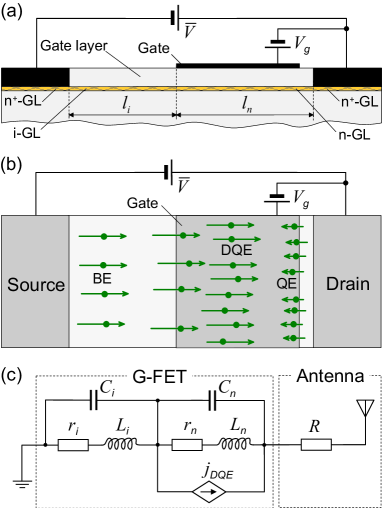
The linearity of the carrier energy dispersion law in graphene determines the specifics of the electron-electron (electron-hole and hole-hole) Coulomb interactions. In particular, it enables a pronounced Coulomb carrier drag [15, 16, 17, 18, 19, 20, 21] and can affect the plasma-electron-beam instability [22]. As demonstrated recently [23], in the lateral n+-i-n-n+ G-FETs with the structure shown in Figs. 1(a) and 1(b), the two-dimensional ballistic electrons (BEs) injected from the source via the i-region into the gated n-region can effectively drag the quasi-equilibrium electrons (QEs) in this region. Due to the BE-QE scattering, the current of the dragged QEs can exceed the current of the injected BEs (the current amplification, schematically shown in Fig. 1(c) as the current depended current source). The latter can cause the reverse injection of the QEs from the drain and affect the G-FET current-voltage (IV) characteristics resulting in their strong nonlinearity [23].
In this paper, we demonstrate that the QE drag by the BEs in the G-FETs can provide the positive feedback between the BE current injected from the source and the QE reverse current. This can enable the instability of the DC current flow in the G-FET channel. Since the QE system in the G-FET can play the role of the THz resonant plasmonic cavity [3, 5], the instability in question can lead to the self-excitation of the THz plasma oscillations feeding an antenna and resulting in the THz radiation. We derive the G-FET source-drain small-signal impedance as a function of the device structural parameters and show that the real part of the G-FET impedance can be negative at the plasma frequency, at which the imaginary part turns zero, that corresponds to the self-excitation of the plasma oscillations [24].
We assume that:
(i) The length, , of the undoped i-region (see Fig. 1(a)) is sufficiently short allowing for the ballistic motion of the injected electrons: , where
cm/s, is the characteristic time of the BE scattering on the acoustic phonons and impurities. In the graphene encapsulated in hBN, this condition can be realized if m at room temperature [25] and in even fairly long graphene layers at reduced temperatures [26];
(ii) The characteristic time, , of the BE-QE collisions is the shortest scattering time in the n-region: , where the latter times are associated with the scattering of the BEs on the optical phonons and other momentum-non-conserving collisions such as those involving impurities;
(iii) Then the energy of the BEs injected into the n-region exceeds the energy of optical phonons ( meV), the pertinent scattering mechanism can substantially dissipate the energy and momentum of the BEs.
When the length of the gated n-region , the majority of the BEs injected into the n-region transfer their energy and, what is crucial, the momentum to the QEs. This causes their drag toward the drain forming the current exceeding the injected current since despite the energy conservation at the electron-electron collisions, the net velocity of the electron system can increase. At the electron densities cm-2 and temperature K for the energy, , of the BEs injected into the n-region about the optical phonon energy meV one can set ps-1 and ps-1 [27] with the QE net scattering time on the acoustic phonons and impurities about ps [28]. The minimization of the BE scattering on impurities in the n-region is possible due to primarily electricstatic doping of this region by the gate voltage. Similar situation can occur in the case of the n-region doping by donors placed sufficiently far away from the channel when is much shorter than the time of the BE collisions with the remote charged impurities.
Considering the G-FET with the equivalent circuit shown in Fig. 1(c) and equalizing the BE current across the i-region and the net currents across the n-region, we arrive at the following equation:
| (1) |
Here and are the densities of the BE and QE currents across the i-region and the gated n-region, accounting for their resistances and kinetic inductivities, and are the displacement currents, and are the potential drops across the i- and the n-regions, respectively. The capacitances are given by (accounting for the specific of the structure [29, 30, 31, 32]) and , where is the dielectric constant of the material in which graphene is embedded, is on the order of unity, is the G-FET width, and is the gate layer thickness.
The drag current density is given by [23] , where is the characteristic current density, is the Coulomb drag factor (which describes the drag current multiplication) with . The exponent is the probability of the optical phonon emission by a BE with the energy , which accounts for the Pauli principle and for the threshold character of such an emission process characterized by the step-like function . The function describes the temperature smearing of the optical phonon emission threshold ( is the Boltzmann constant).
At the dc bias voltage applied between the source and drain contacts and the dc voltage drop across the i-region, the source-drain current density is equal to and . Here is the i-region dc conductivity in the ”virtual cathode” approximation [29] and is the drift (Drude) conductivity of the n-region, where , , and are the QE density, scattering time, and fictitious effective mass. In this case, considering that ( is the electron charge) and introducing the normalized current density , from Eq. (1) we arrive at the following equation relating and :
| (2) |
Here is the ratio of the i- and n-regions resistances , , and . Equation (2) describes the monotonic and the S-shaped IV characteristics at and , respectively [23].
Considering the G-FET dynamic response, we assume that the voltages and comprise the ac components: and , where is the signal frequency, and the normalized source-drain current also includes the pertinent ac contribution .
In this case, in the linearized version of Eq. (1) we put and , where and determine the pertinent regions kinetic inductance. The scattering time coincide with the ratio of the n-region inductance and resistance. Since the transit time of the BEs across the i-region is short, the i-region kinetic ballistic inductance can be disregarded. We also disregard the displacement current across the i-region due to . This is justified in the range of frequencies under consideration. The voltage drop across the G-FET can be expressed via the net ac voltage , as , where is the emitting antenna radiation resistance.
As a result, from Eq. (1) for the ac component of the normalized current we obtain the following equation:
| (3) |
Here
| (4) |
is the net impedance of the loop circuit under consideration. Deriving Eqs. (3) and (4), we have introduced the quantities: , , which depend on the parameters and , and the plasma frequency
| (5) |
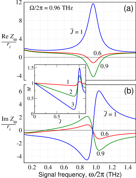
Here is the QE Fermi energy. The plasma frequency given by Eq. (5) corresponds to its standard value for the plasma wavelength . Setting meV, , cm, and cm, we obtain THz.
In the range of low frequencies , Eq. (4) yields (in the absence of the Coulomb drug, and ) and (when the drug is pronounced, ).
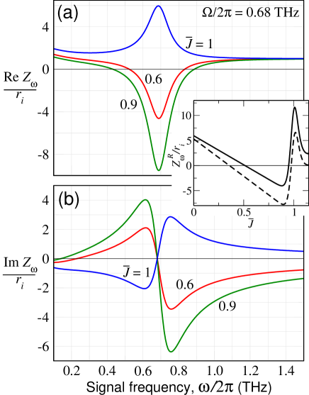
At the plasmonic resonance , the impedance imaginary part becomes zero, and Eq. (4) yields
| (6) |
Equation (6) yields the condition in the following forms:
| (7) |
Considering that , inequality (7) can be presented as
| (8) |
The latter condition is valid at not too small (). As follows from Eqs. (7) and (8), the instability criteria primarily requires a sufficiently large value , i.e., not too large . This implies a relatively strong Coulomb electron drag.
Figures 2 and 3 show the real part Re and the imaginary part Im of normalized impedance versus signal frequency calculated for different values of the normalized bias current using Eq. (4) and the versus dependence shown in the inset in Fig.2. The resonant impedance as a function of the normalized bias current calculated using Eq. (6) is shown in the inset in Fig. 3. The structural parameters used for Figs. 2 and 3 correspond to realistic values: cm, cm, cm, , , and . For these parameters, assuming that the G-FET width cm, we obtain s/cm = 47 - 71 Ohm. This implies that at the realistic parameters of the G-FET structure, the resistance can match the standard antenna radiation resistance. When , i.e., mV, in a G-FET with the above parameters the dc current mA.
One can see that at selected structural parameters and the bias current (bias voltage), Re in the THz range. Just in the range, where Re , Im changes its sign turning zero at the plasmonic resonance. This corresponds to the self-excitation of high-frequency oscillations [24] - the plasma oscillations in our case, followed by the radiation emission from the antenna.
In conclusions, we predicted the possibility of the current driven plasma instability in the lateral G-FETs with the BE injection into the gated n-region region and the Coulomb drag of the QE by the BEs. The plasma instability and the pertinent self-excitation of the THz oscillation are associated with the amplification of the current due to the transfer of the BE momentum to the QEs. The plasma oscillations self-excitation can lead to the THz radiation emission using the proper antenna. The G-FETs under consideration can be connected in series forming a periodic lateral structure (like in Ref. [11, 33]) that can enhance the THz emission.
The work at RIEC and UoA was supported by the Japan Society for Promotion of Science (KAKENHI Nos. 21H04546, 20K20349), Japan; and the RIEC Nation-Wide Collaborative research Project No. H31/A01, Japan. The work at RPI was supported by the Office of Naval Research (N000141712976, Project Monitor Dr. Paul Maki).
Data Availability
The data that support the findings of this study are available from the corresponding author upon reasonable request.
References
- [1] A. V. Chaplik, “Possible crystallization of charge carriers in low-density inversion layers,”Sov. Phys. JETP 35, 395 (1972).
- [2] M. Dyakonov and M. Shur, “Shallow water analogy for a ballistic field effect 317 transistor. New mechanism of plasma wave generation by DC current,”Phys. Rev. Lett. 71, 2465 (1993).
- [3] M. I. Dyakonov and M. S Shur, ‘Plasma wave electronics: novel terahertz devices using two-dimensional electron fluid,”IEEE Trans. Electron. Devices 43, 1640 (1996).
- [4] G. R. Aizin, J. Mikalopas, and M. Shur, “Plasmonic instabilities in two-dimensional electron channels of variable width,”Phys. Rev. B 101, 245404(2020).
- [5] V. Ryzhii, A. Satou, and T. Otsuji, “Plasma waves in two-dimensional electron-hole system in gated graphene,”J. Appl. Phys. 101, 024509 (2007).
- [6] V. Ryzhii, T. Otsuji, M. Ryzhii, and M. S. Shur, “Double graphene-layer plasma resonances terahertz detector,”J. Phys. D: Appl. Phys. 45, 302001 (2012).
- [7] T. Otsuji, T. Watanabe, S. A. Boubanga Tombet, A. Satou, W. M. Knap, V. V. Popov, M. Ryzhii, and V. Ryzhii, “Emission and detection of terahertz radiation using two-dimensional electrons in III–V semiconductors and graphene,”IEEE Trans. Terahertz Sci. Technol. 3, 63 – 71 (2013).
- [8] D. Yadav, S. Boubanga-Tombet, T. Watanabe, S. Arnold, V. Ryzhii, and T. Otsuji, “Terahertz wave generation and detection in double-graphene layered van der Waals heterostructures,”2D Matter. 3, 045009 (2016).
- [9] V. Ryzhii, M. Ryzhii, M. S. Shur, V. Mitin, A. Satou, and T. Otsuji, “Resonant plasmonic terahertz detection in graphene split-gate field-effect transistors with lateral p-n junctions,”J. Phys. D: Appl. Phys. 49, 315103 (2016).
- [10] D. Svintsov, “Emission of plasmons by drifting Dirac electrons: A hallmark of hydrodynamic transport,”Phys. Rev. B 100, 195428 (2019).
- [11] J. A. Delgado-Notario, V. Clericò, E. Diez, J. E. Velazquez-Perez, T. Taniguchi, K. Watanabe, T. Otsuji, and Y. M. Meziani, “Asymmetric dual grating gates graphene FET for detection of terahertz radiations,”APL Photon. 5, 066102 (2020).
- [12] I. M. Moiseenko, V. V. Popov, and D. V. Fateev, “Terahertz plasmon amplification in a double-layer graphene structure with direct electric current in hydrodynamic regime,”Phys. Rev. B 103, 195430 (2021).
- [13] I. Gayduchenko, S. G. Xu, G. Alymov, M. Moskotin, I. Tretyakov, T. Taniguchi, K. Watanabe, G. Goltsman, A. K. Geim, G. Fedorov, D. Svintsov and D. A. Bandurin, “Tunnel field-effect transistors for sensitive terahertz detection,”Nat. Comm. 12, 543 (2021).
- [14] V. Ryzhii, T. Otsuji, and M. S. Shur, “Graphene based plasma-wave devices for terahertz applications, ”Appl. Phys. Lett. 116, 140501 (2020).
- [15] V. Vyurkov and V. Ryzhii, “Effect of Coulomb scattering on graphene conductivity,”JETP Lett. 88, 370 (2008).
- [16] X. Li, E. A. Barry, J. M. Zavada, M. Buongiorno Nardelli, and K. W. Kim, “Influence of electron-electron scattering on transport characteristics in monolayer graphene,”Appl. Phys. Lett. 97, 082101 (2010).
- [17] R. V. Gorbachev, A. K. Geim, M. I. Katsnelson, K. S. Novoselov, T. Tudorovskiy, I. V. Grigorieva, A. H. MacDonald, S. V. Morozov, K. Watanabe, T. Taniguchi, and L. A. Ponomarenko, “Strong Coulomb drag and broken symmetry in double-layer graphene,”Nat. Phys. 8, 896 (2012).
- [18] D. Svintsov, V. Vyurkov, S. Yurchenko, T. Otsuji, and V. Ryzhii, “Hydrodynamic model for electron-hole plasma in graphene,”J. Appl. Phys. 111, 083715 (2012).
- [19] J. C. Song, D. A. Abanin, and L. S. Levitov, “Coulomb drag mechanisms in graphene,”Nano Lett. 13, 3631 (2013).
- [20] M. Schütt, P. M. Ostrovsky, M. Titov, I. V. Gornyi, B. N. Narozhny, and A. D. Mirlin, “Coulomb drag in graphene near the Dirac point,”Phys. Rev. Lett. 110, 026601 (2013).
- [21] D. Svintsov, V. Vyurkov, V. Ryzhii, and T. Otsuji, “Hydrodynamic electron transport and nonlinear waves in graphene, ”Phys. Rev. B 88, 245444 (2013).
- [22] D. Svintsov, “Fate of an electron beam in graphene: Coulomb relaxation or plasma instability,”Phys. Rev. B 101, 235440 (2020).
- [23] V. Ryzhii, M. Ryzhii, V. Mitin, M. S. Shur, and T. Otsuji, “S-shaped current-voltage characteristics of n+-i-n-n+ graphene field-effect transistors due to the Coulomb drag of quasi-equilibrium electrons by ballistic electrons,”Phys. Rev. Appl. , in press (2021).
- [24] G. I. Haddad, J. R. East, and H. Eisele, “Two-terminal active devices for terahertz sources,”Int. J. High Speed Electron. Syst. 13, 395-427 (2003).
- [25] A. S. Mayorov, R. V. Gorbachev, S. V. Morozov, L. Britnell, R. Jalil, L. A. Ponomarenko, P. Blake, K. S. Novoselov, K. Watanabe, T. Taniguchi, and A. K. Geim, “Micrometer-scale ballistic transport in encapsulated graphene at room temperature,”Nano Lett. 11, 2396 (2011).
- [26] L. Banszerus, M. Schmitz, S. Engels, M. Goldsche, K. Watanabe, T. Taniguchi, B. Beschoten, and C. Stampfer, “Ballistic transport exceeding 28 m in CVD grown graphene,”Nano Lett. 16, 1387 (2016).
- [27] M. V Fischetti, J Kim, S. Narayanan, Zh.-Y. Ong, C. Sachs, D. K. Ferry, and S. J. Aboud, “Pseudopotential-based studies of electron transport in graphene and graphene nanoribbons,”J. Phys: Cond. Mat. 25, No.47 (2013).
- [28] D. A. Bandurin, I. Torre, R. Krishna Kumar, M. Ben Shalom, A. Tomadin, A. Principi, G. H. Auton, E. Khestanova1, K. S. NovoseIov, I. V. Grigorieva, L. A. Ponomarenko, A. K. Geim, and M. Polini, “1 Negative local resistance due to viscous electron backflow in graphene,”Science 351, 1055-1058 (2016).
- [29] A. Grinberg, S. Luryi, M. Pinto, and N. Schryer, “Space charge- limited current in a film,”IEEE Trans. Electron Devices 36, 1162 (1989).
- [30] S. G. Petrosyan and A. Ya. Shik, “Contact phenomena in low-dimensional electron systems,”Sov. Phys. JETP 69, 1261 (1989).
- [31] B. Gelmont, M. Shur, and C. Moglestue, “Theory of Junction Between Two-Dimensional Electron Gas and p-Type Semiconductor,”IEEE Trans. on Electron Devices 39, 1216 (1992).
- [32] D. B. Chklovskii, B. I. Shklovskii, and L. I. Glazman, “Electrostatics of edge channels,”Phys. Rev. B 46, 4026 (1992).
- [33] T. A. Elkhatib, V. Y. Kachorovskii, W. J. Stillman, D. B. Veksler, K. N. Salama, Xi-Ch. Zhang, and M. S. Shur, “Enhanced plasma wave detection of terahertz radiation using multiple high electron-mobility transistors connected in series,”IEEE Trans. Microw. Theory Techn. 58, 331-339 (2010).