Performance Studies of the ATLASpix HV-MAPS Prototype for Different Substrate Resistivities
Abstract
The ATLASpix high-voltage monolithic active pixel sensor (HV-MAPS) was designed as a technology demonstrator for the ATLAS ITk Upgrade and the CLIC tracking detector. In this contribution new results from laboratory-based energy calibration measurements using fluorescence X-rays are presented for the ATLASpix_Simple matrix. These findings are complemented by new results from test-beam studies with inclined tracks, in which the active charge collection depth is determined.
1 Introduction
The experimental conditions at future high-energy particle physics experiments, such as the High-Luminosity Large Hadron Collider (HL-LHC) [1] or the Compact Linear Collider (CLIC) [2], require highly performant detector systems to meet the foreseen physics goals. Due to the advances in the silicon sensor industry, all-silicon detector systems are regarded attractive options for future tracking detectors. Monolithic technologies combine both the sensor and the readout electronics on one chip, resulting in a reduced material budget compared to hybrid technologies. They are considered particularly suitable for large-area applications due to their cost efficiency and large-scale production capabilities of the CMOS imaging industry.
The ATLASpix [3] was designed as a technology demonstrator for the ATLAS ITk upgrade [4] and the CLIC tracking detector [5]. It was manufactured in a commercial HV-CMOS process on wafers with different substrate resitivities ranging from to . As a high-voltage monolithic active pixel sensor (HV-MAPS), it features a fully integrated readout. A high bias voltage of leads to large signals due to a large depleted volume, as well as a high electric field resulting in fast charge collection via drift. By removing bulk material from the backside, the sensors can be thinned to . The active matrix of the ATLASpix_Simple consists of 25 columns and 400 rows of pixel cells with a pitch of , which are read out in a zero-suppressed triggerless column drain scheme. Each pixel consists of a deep N-well in a p-substrate forming the sensor diode. The N-well contains the in-pixel electronics comprising a charge-sensitive amplifier and a comparator. For each hit, the time-of-arrival (ToA) with a resolution of and a binning of , as well as the time-over-threshold (ToT) with a 6-bit resolution are recorded.
2 Energy Calibration with Fluorescence X-Rays
In order to perform an energy calibration of the detection threshold and the time-over-threshold (ToT) measurement, the ATLASpix_Simple samples were exposed to X-rays with well-defined energies. A commercial X-ray tube was used to excite fluorescence a target placed in front of the X-ray tube. By choosing different target materials (titanium, iron, copper), sharp peaks with well-defined energies were generated to which the ATLASpix_Simple were exposed.
2.1 Analysis Method
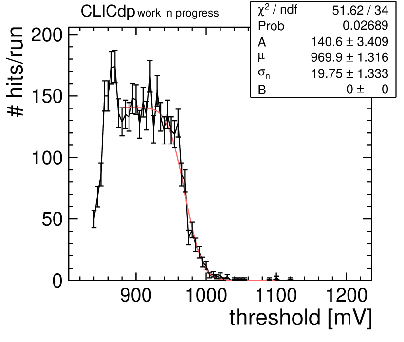
For each pixel of the matrix, the number of pixel hits per run of is plotted against the threshold. This yields a distribution as shown in Figure 1(a), which can be described by a so-called s-curve:
| (1) |
where is a normalisation constant, is the threshold value corresponding to the mean signal of the X-ray, and represents the pixel noise arising from fluctuations of the baseline and the threshold. is an offset to account for a high-energy contamination of the measured spectrum from primary X-rays Compton-scattered at the target, which are observed for the low energy X-rays from titanium. For higher energies, it is set to zero. At very low thresholds, the hit count drops significantly due to an over-saturation of the readout caused by a strongly rising noise rate. Consequently, this region is excluded from the fit of the s-curve.
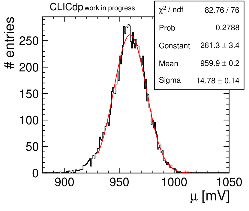
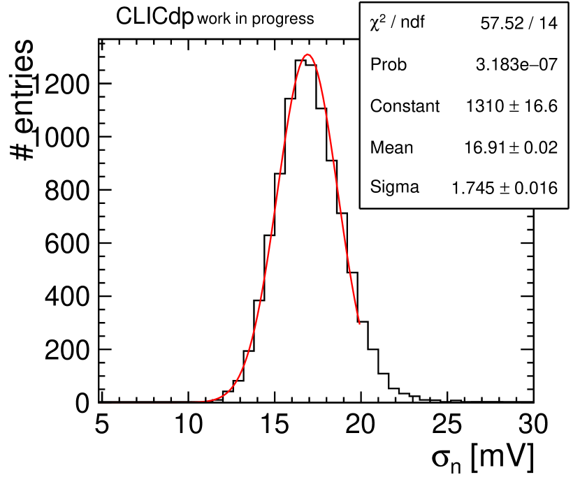
The resulting and from the fit function are filled into histograms as shown in Figures 1(b) and 1(c), which contain one entry from the fits to the s-curve of each pixel in the matrix. The histograms show normal distributions, which are fitted with a Gaussian to obtain the mean and the spread of each distribution: and . The non-gaussian tails visible on the left in Figure 1(b) and on the right in Figure 1(c) originate from noisy pixels.
2.2 Gain and Baseline
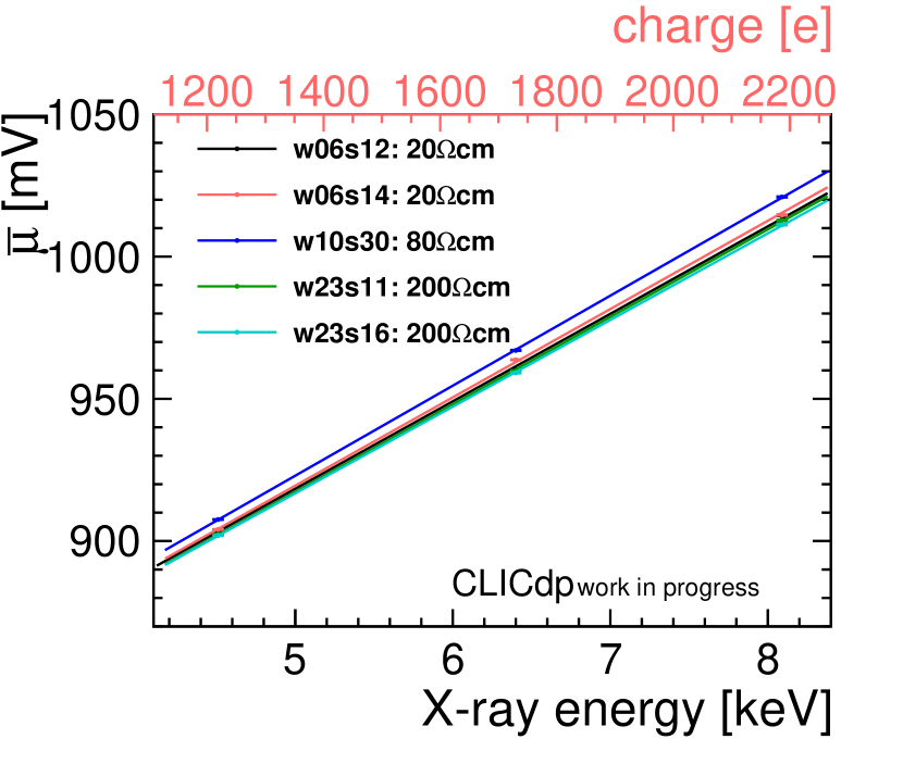
Since soft X-rays are absorbed completely, the amount of deposited energy is well-defined and can be converted into the signal charge corresponding to the number of created electron-hole pairs. An average energy of is required to generate one electron-hole pair [6]. Figure 2(a) shows the values obtained for the different X-ray targets. A first-order polynomial is fitted for all samples:
| (2) |
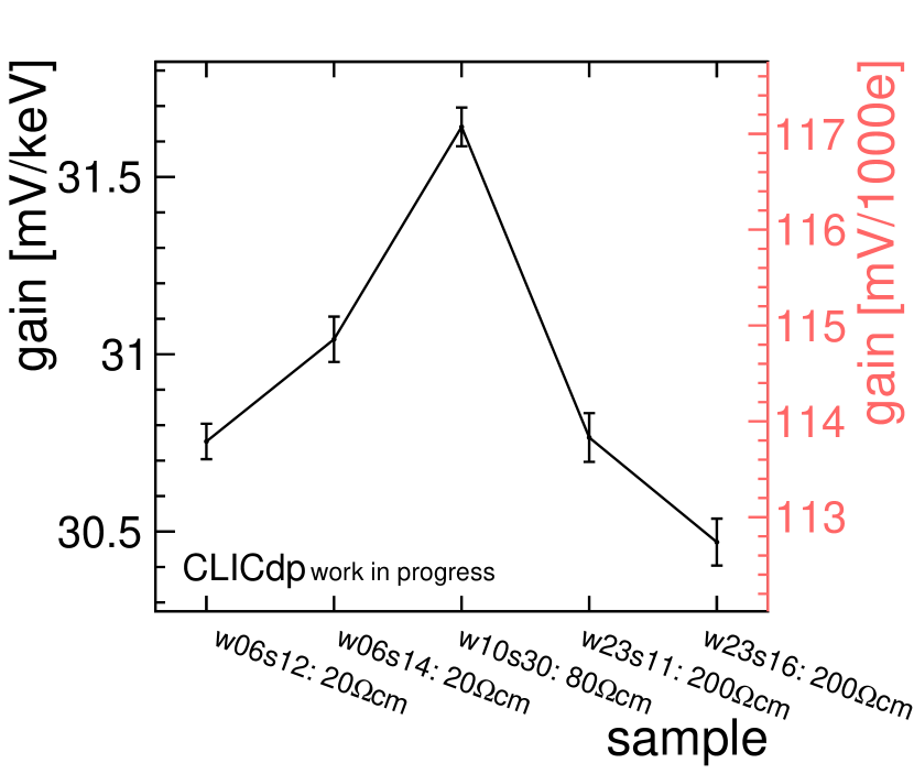
where denotes the extrapolated baseline, i.e. the -intercept of the polynomial. The slope of the fit function can be interpreted as the signal gain, which is summarised in Figure 2(b) for all presented samples. Since no clear trend of the gain with the substrate resistivity can be seen, it can be concluded that the observed differences stem from sample-to-sample or wafer-to-wafer variations and are dominated by the electronics.
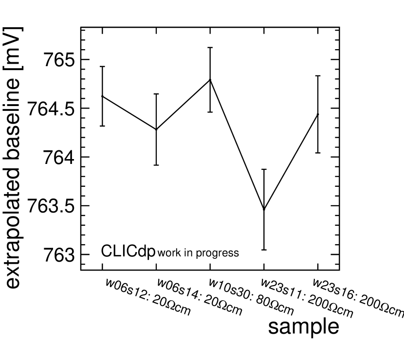
Figure 2(c) summarises the extrapolated baseline, i.e. the -intercept of the linear fit functions for all samples. It is observed that it differs notably from the externally applied baseline of . This effect is consistent with an expected voltage offset within the in-pixel comparator, which can be [7].
The inversion of Equation 2 can be used to determine the signal charge for a given threshold:
| (3) |
with the statistical uncertainty obtained by Gaussian error propagation.
Averaging over all samples a gain of and an extrapolated baseline of have been measured. It is important to note that the gain strongly depends on the chip configuration, in particular those parameters which regulate the current of the charge-sensitive amplifier in the pixel.
Using the gain as a conversion factor, the threshold dispersion and the pixel noise determined previously can now be translated into an equivalent charge. The standard deviation is the threshold dispersion, i.e. the variation of the the detection threshold across the pixel matrix. The mean of is the average pixel noise. For an energy deposition of , this results in a signal-to-noise ratio of
| (4) |
3 Test-beam Performance Measurements
Performance measurements of the ATLASpix_Simple have been carried out at the DESY-II test-beam facility [8] using EUDET-type reference telescopes [9]. For the chosen electron beam momentum of , these yield a track pointing resolution of , depending on the plane spacing, which allows to study in-pixel effects. With an additional Timepix3 plane [10], a track time resolution of is achieved. The ATLASpix_Simple was controlled and read out with the Caribou system [11], and the reconstruction and analysis was carried out using the Corryvreckan framework [12].
3.1 Spatial and Time Resolution and Hit Detection Efficiency
Previous studies [13] have shown that the ATLASpix_Simple reaches a binary spatial resolution limited by its pixel pitch and a timing resolution down to for the samples after a row-dependent delay and a timewalk correction. Lower substrate resistivities lead to a slower timing. Samples with all substrate resistivities can be operated at a high detection efficiency above , whereas the efficiency at high thresholds and low bias voltages remains larger for higher substrate resistivities.
3.2 Active Depth Determination
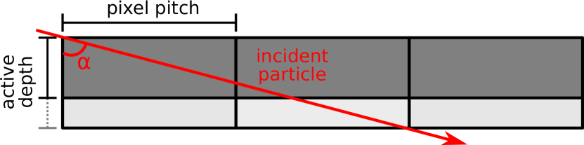
Inclined tracks are expected to lead to increased cluster sizes because a particle penetrates several adjacent pixels while passing through the detector material. As illustrated in Figure 4, this is dependent on the incidence angle as well as the pixel pitch and the active depth . Here, the active depth refers to the depleted volume plus a possible additional layer below the depletion depth, from which charge may be collected by diffusion into the depletion region. In this simple geometrical model, the average cluster width in column/row direction is given by
| (5) |
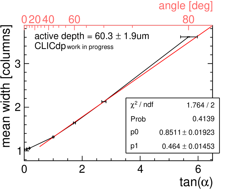
In turn, a measurement of the angle dependence of the cluster size can be used to obtain an estimation of the active depth. This represents a simplified model, which neglects possible sub-threshold effects as well as lateral diffusion. This is an appropriate approximation for the ATLASpix_Simple, for which the mean cluster size is only marginally larger than one [14].
Figure 4 shows the mean cluster width in column direction plotted against the tangent of the rotation angle. Using equation 5, the active depth can be retrieved from the slope of a linear fit by dividing through the pixel pitch in the respective dimension. This yields an estimation of at a bias voltage of . The comparison with TCAD studies [15] suggests that the substrate resistivity lies around compared to the nominal value of . A possible range of is stated by the manufacturer due to deviations of the production parameters from the standard process [16].
4 Conclusions
It was shown that an X-ray based calibration is crucial for the the conversion of the detection threshold and noise from an applied voltage to equivalent charge. A higher substrate resistivity yields a higher efficiency and a better time resolution. The determination of the active depth implies that the substrate resistivity exceeds in accordance with TCAD simulations [15].
The obtained results confirm that HV-MAPS is a suitable technology for future tracking detectors. It is now also investigated as a candidate technology for other experiments such as the MightyTracker Project for the LHCb Upgrades Ib and II [17].
The measurements leading to these results have been performed at the Test Beam Facility at DESY Hamburg (Germany), a member of the Helmholtz Association (HGF).
This work has been sponsored by the Wolfgang Gentner Programme of the German Federal Ministry of Education and Research (grant no. 05E15CHA and 05E18CHA).
References
References
- [1] Apollinari G, Béjar Alonso I, Brüning O et al. 2017 High-Luminosity Large Hadron Collider (HL-LHC): Technical Design Report V. 0.1 CERN Yellow Report URL https://cds.cern.ch/record/2284929
- [2] Burrows P, Lasheras N, Linssen L et al. (eds) 2018 The Compact Linear Collider (CLIC) - 2018 Summary Report CERN Yellow Report URL https://cds.cern.ch/record/2652188
- [3] Perić I et al. 2019 Nucl. Instrum. Meth. A924 99–103
- [4] Prathapan M et al. 2019 PoS TWEPP2018 074
- [5] Dannheim D, Krüger K, Levy A et al. (eds) 2019 Detector technologies for CLIC CERN Yellow Report URL https://cds.cern.ch/record/2673779
- [6] Fraser G, Abbey A, Holland A, McCarthy K, Owens A and Wells A 1994 Nucl. Instrum. Meth. A350 368–378
- [7] Perić I 2021 Private communication
- [8] Diener R et al. 2019 Nucl. Instrum. Meth. A922 265–286
- [9] Jansen H et al. 2016 EPJ Tech. Instrum. 3 7
- [10] Poikela T et al. 2014 JINST 9 C05013
- [11] Vanat T 2020 PoS TWEPP2019 100
- [12] Dannheim D et al. 2021 JINST 16 P03008
- [13] Kröger J 2020 JINST 15 C08005
- [14] Kröger J Characterisation of a High-Voltage Monolithic Active Pixel Sensor Prototype for Future Collider Detectors Ph.D. thesis (in preparation) Heidelberg University
- [15] González A M Ph.D. thesis (in preparation) Heidelberg University
- [16] Perić I et al. 2018 Description of the ATLASPix Simple and ATLASPIX M2 Preliminary v2 (unpublished)
- [17] Blanc F 2020 the LHCb Mighty Tracker URL https://cds.cern.ch/record/2744243