High-contrast plasmonic-enhanced shallow spin defects in hexagonal boron nitride for quantum sensing
Abstract
The recently discovered spin defects in hexagonal boron nitride (hBN), a layered van der Waals material, have great potential in quantum sensing. However, the photoluminescence and the contrast of the optically detected magnetic resonance (ODMR) of hBN spin defects are relatively low so far, which limits their sensitivity. Here we report a record-high ODMR contrast of 46 at room temperature, and simultaneous enhancement of the photoluminescence of hBN spin defects by up to 17-fold by the surface plasmon of a gold-film microwave waveguide. Our results are obtained with shallow boron vacancy spin defects in hBN nanosheets created by low-energy He+ ion implantation, and a gold-film microwave waveguide fabricated by photolithography. We also explore the effects of microwave and laser powers on the ODMR, and improve the sensitivity of hBN spin defects for magnetic field detection. Our results support the promising potential of hBN spin defects for nanoscale quantum sensing.
Optically active spin defects in wide-band-gap materials have shown great potential for a wide range of emerging technologies, from quantum information processing [1, 2] to high-resolution sensing of magnetic and electric fields[3, 4, 5, 6]. Color centers in bulk semiconductors such as diamond [7, 8] and silicon carbide[9, 10] are prime examples that reveal optically detected magnetic resonance (ODMR). Recently, atomic defects in layered van der Waals materials such as hexagonal boron nitride (hBN) are attracting increasing attention as alternative candidates for studying light-matter interaction, nanophotonics and nanoscale sensing[11, 12, 13, 14]. Atomic defects in hBN are stable in nanosheets as thin as a monolayer and are readily accessible for device integration and top down nanofabrication [15, 16]. Furthermore, recent experiments discovered that some defects in hBN could be spin addressable at room temperature[17, 18, 19, 20, 21]. The negatively charged boron vacancy () spin defect is the most studied one among these defects [22, 23]. It has spin and its orientation is out of plane [17]. defects can be generated by neutron irradiation [17, 24], ion implantation[25], femtosecond laser writing [26], and electron irradiation [27]. Spin defects in thin hBN nanosheets will be useful for quantum sensing and spin optomechanics [28, 29]. However, so far the spin defects have relatively low brightness and ODMR contrast, which limit their sensitivity [21].
Here we report high-contrast plasmonic-enhanced shallow spin defects in hBN nanosheets for quantum sensing. We fabricate a gold-film coplanar microwave waveguide by photolithography to optimize the homogeneity and local intensity of the microwave for spin control. The hBN nanosheets with spin defects are transferred onto the microwave waveguide and are in contact of the gold surface for both plasmonic emission enhancement and spin control. The surface plasmons [30, 31, 32] provide broadband emission enhancement covering the wide range of the photoluminescence (PL) of defects from 750 nm to 950 nm [17]. Our method does not require complex nanofabrication or cause adverse effects on quantum sensing. The microwave magnetic field generated by the gold waveguide is parallel to the surface and perpendicular to the orientation of electron spins, which is crucial to achieve high ODMR contrast. With these, we find that the ODMR contrast can reach 46 at room temperature, which is an order of magnitude larger than the highest room-temperature ODMR contrast of hBN spin defects reported in the previous work [33]. We also observe an up to 17-fold photoluminescence (PL) enhancement of defects due to the gold film. We measure the spin initialization time to be around 100 ns. In addition, we study the laser power and microwave power dependence of the continuous-wave (CW) ODMR, and optimize the magnetic field sensitivity to be about 8 . Finally, we perform coherent spin control and measure the spin-lattice relaxation time and the spin coherence time of spin defects generated by He+ ion implantation, which can benefit future works on multi-pulse sensing protocols. Our results demonstrate the promising potential of hBN spin defects for nanoscale quantum sensing and other quantum technologies.
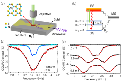
The results presented in this work are obtained with tape-exfoliated hBN nanosheets which are tens of nanometers thick. We exfoliate hBN flakes onto a Si wafer, and then mount the wafer in a home-built ion implanter for doping. We use low-energy He+ ions (200 eV - 3 keV) to implant hBN nanosheets, which creates high-quality defects with average depths ranging from 3 nm to 30 nm and avoids introducing undesired defects [34]. After ion implantation, the hBN flakes are transferred onto a gold microwave stripline on a sapphire substrate and characterized using an ODMR setup (Fig. 1 (a)). CW ODMR measurements are performed to acquire the basic spin properties of the defects generated by He+ ions. The defects are excited by a 532 nm laser with an NA=0.9 objective lens, which also collects the PL of defects. We record integrated photon counts as a function of the applied microwave. We obtain the difference between the photon count rates when the microwave is off () and when the microwave is on (). The ODMR contrast is then determined by normalizing the PL difference with the PL intensity when the microwave is off: . A positive ODMR contrast means that the microwave driving decreases the PL intensity.
Figure 1(c) shows measured high-contrast ODMR spectra of defects at room temperature. Strikingly, with strong microwave driving, we find that these defects can exhibit up to 46 ODMR contrast, which is one order of magnitude higher than the best contrast of hBN spin defects reported previously [33]. This value is even larger than the ODMR contrast of diamond nitrogen-vacancy centers at room temperature [7]. The ODMR contrast can readily reach around 20 without significant power broadening using low-power microwave driving. Without an external magnetic field, the measured ODMR spectrum shows two resonances at and centered around (Fig. 1(c)). The results agree well with a double Lorentzian model. Here is determined by the zero-field splitting (ZFS), = 3.47 GHz, where is the Planck constant. And the splitting between and is due to the non-zero off-axial ZFS parameter 50 MHz [17]. Fig. 1 (d) presents ODMR spectra in different external static magnetic fields. We use a permanent magnet to apply a static magnetic field perpendicular to the nanosheet surface. A translation stage is used to change the position of the magnet and tune the magnetic field strength. With an external static magnetic field , and will be split further owing to the Zeeman effect, , where is the Landé -factor. The splitting () is 560 MHz (346 MHz) at 9.8 mT (5.9 mT).
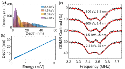
It is highly desirable to create spin defects as close to surface as possible without degrading the spin properties for nanoscale quantum sensing. This can decrease the ultimate distance between a sample and the sensor, which can significantly improve the signal. In Fig. 2, we study the formation of shallow defects by using He+ ions. First, we use the Stopping and Range of Ions in Matter (SRIM) software to calculate the depths and densities of vacancies created with different ion energies from 200 eV to 3 keV (Fig. 2 (a),(b)). The most probable depth is 3.5 nm, 6.4 nm, 15 nm, and 25 nm when the He+ ion energy is 300 eV, 600 eV, 1.5 keV, and 2.5 keV, respectively. Then we perform the CW ODMR measurements on the samples with different doping depths. Here we use weak microwave driving to avoid the power broadening. So we can extract the nature linewidth of defects (Fig. 2 (c)). All the ODMR spectra display similar linewidths as well as the contrasts, indicating the hBN spin properties are nearly the same at different doping depths.
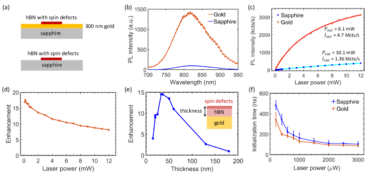
For sensing applications, the PL brightness is an important factor that directly affects the sensitivity. Former theoretical studies indicate that the near-infrared optical transition of defects is not an electric dipole-allowed transition and is hence relatively dark [22, 23]. In this context, improving their brightness is a crucial task. Here we utilize surface plasmons of a metallic film[30, 31, 32] to enhance the brightness of the . Surface plasmons are collective oscillations of coupled eletromagnetic waves and free electrons on metallic surfaces. They have large localized electric and magnetic fields which can speed up both radiative and nonradiative decays. We choose plasmonic enhancement because it can cover the whole broad PL spectral range of defects. In addition, this method can utilize the metallic surface of our microwave waveguide and does not require complex nanofabrication. Our microwave waveguide is made of a 300-nm thick gold film prepared by electron-beam physical vapor deposition on top of a sapphire wafer. The width of the center microstrip is 50 m. The hBN flakes with defects are transferred onto both the gold film and the sapphire substrate for comparison (Fig. 3 (a)). defects on both gold and sapphire surfaces display broad PL emission spectra around 810 nm (Fig. 3 (b)). Remarkably, the defects on the gold film shows an order of magnitude higher PL intensity than those on the sapphire substrate under the same laser excitation. Fig. 3 (c) and (d) present the PL intensities of these two samples and their PL ratio at different laser excitation powers. The experimental data in Fig. 3 (c) is fit to , where is the PL intensity of the , is the saturation PL intensity, is the excitation laser power, and is the saturation laser power. On a gold film, the defects show up to 17-fold enhancement of PL intensities under low-power excitation. We also observe a strong modification of the saturation behavior (Fig. 3 (c)). The laser saturation power is reduced by a factor of 5 and the saturation PL count rate is increased by around 3.5 times. These indicate that a gold film can improve the quantum efficiency of defects significantly.
We also study the effect of the separation between the gold film and defects on the brightness enhancement. We transfer hBN flakes with different thickness onto the gold micostrip, so that we can get various distances between the defects and the gold film. The thickness of hBN nanosheets is measured by an atomic force microscope (AFM). The PL intensities are measured before and after transfer. Here we use 600 eV He+ ions to generate shallow with a most probable depth of 6.4 nm. So the average separation between the gold film and defects is equal to the thickness of hBN nanosheets subtracted by 6.4 nm. As a result, we observe a strong thickness dependence of the PL enhancement. The highest enhancement is obtained when the hBN flake thickness is around 35 nm. Our result is consistent with the former result on plasmonic enhancement of quantum dots on a gold surface [31]. When a hBN nanosheet is too thin, the nonradiative decay dominates. There is also little brightness enhancement when the hBN nanosheet is too thick because the surface plasmonic modes decay exponentially away from the surface. So there is an optimal thickness for plasmonic enhancement. In addition, we characterize the electron spin initialization time of defects on both gold and sapphire surfaces as a function of the power of the 532 nm excitation laser (see the “Supporting Information” for more details). We find that the required spin initialization time is on the order of 100 ns. The gold film reduces the spin initialization time (Fig. 3(f)), which also speeds up quantum sensing.
Sensitivity is the most important parameter to determine the performance of a sensor. To measure an external static magnetic field with spin defects, a common way is to use CW ODMR to detect the Zeeman shifts of the spin sublevels caused by the magnetic field [5]. The precision to determine the magnetic field is directly affected by the photon count rate , the ODMR contrast and the linewidth , following the equation [35]
| (1) |
where is the Bohr magneton. In this expression, is a numerical parameter related to the specific lineshape function. For a Lorentzian profile, 0.77. The values of , and are further related to the microwave power and laser power [35] (see “Supporting Information”). To improve the detection sensitivity, it is crucial to increase the count rate and contrast as high as possible without significant power broadening of the linewidth.
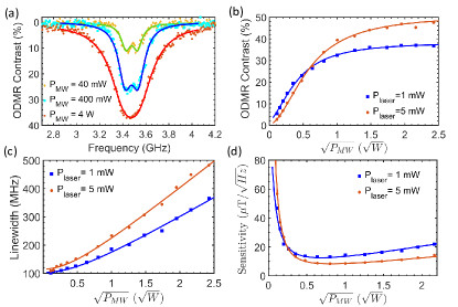
Here we perform a group of CW ODMR measurements with various microwave powers and laser powers to find the optimal conditions for magnetic field sensing (Fig. 4). Fig. 4 (a) presents three typical CW ODMR spectra at different microwave powers. Under low-power 40 mW microwave driving, we obtain an ODMR contrast of 10. Such a low microwave power does not induce significant spectral power broadening. A natural linewidth can be extracted as 110 MHz. With an increasing microwave power, we first observe a significant improvement of the contrast without much spectral broadening. When we increase the microwave power further, the linewidth broadening becomes severe. Fig. 4 (b)-(d) present the quantitative measurements of the ODMR contrast, linewidth and sensitivity as functions of the microwave power. The experimental results fit well with theoretical models as discussed in the Supporting Information. Here we perform the experiments at two different laser powers (1 mW and 5 mW). The 5 mW laser excitation gives a broader linewidth but a higher saturation ODMR contrast compared to those with 1 mW laser excitation. As a result, if we increase the microwave power, the sensitivity is first improved owing to the increase of the ODMR contrast and then becomes worse when the spectral power broadening dominates. The best sensitivity that we have achieved is about 8 . This sensitivity is 10 times better than the former result with hBN spin defects (our system also has a better spatial resolution) [21]. This sensitivity will be enough for studying many interesting phenomena in magnetic materials. For example, the magnetic field generated by a monolayer CrI3 (a 2D van der Waals magnet) is on the order of 200 [6].
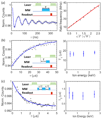
Finally, we perform pulsed ODMR measurements to determine the spin-lattice relaxation time and the spin coherence time of the shallow defects generated by ion implantation. and of hBN spin defects have only been measured for neutron irradiated samples before [19, 24]. It will be useful to know their values for our shallow spin defects created by ion implantation. In addition, pulsed ODMR measurements are inevitable steps for realizing more complex sensing protocols. A pulsed ODMR measurement consists of optical initialization of the ground state, coherent manipulation of the spin state with microwave pulses, and optical readout of the final spin state. Here we add an external magnetic field of 13 mT to split two branches of the spin sublevels. ms = 1,0 states are used as the two-level spin system to carry out the spin coherent control. Fig. 5 (a) shows the Rabi oscillation as a function of the microwave power. The data is fit using . We observe an oscillation with two Rabi frequencies, which are in the tens of megahertz range. The exponential decay of one oscillation component gives the spin-dephasing time of = 120 ns. To gain more insights of the spin properties of the defects at different depths, we measure the spin-lattice relaxation times and spin-spin relaxation times of the defects created with different ion implantation energies. The pulse sequences are shown as insets in the left panels of Fig. 5 (b),(c). By fitting the results, and are obtained as 17 and 1.1 , respectively. As shown in Fig. 5 (b),(c), both and are independent of the ion energy, indicating the spin properties of the defects are nearly independent of the depth.
In conclusion, we have realized a significant improvement of the ODMR contrast and the brightness of hBN spin defects. We observe a record-high ODMR contrast of 46, which is one order of magnitude higher than the best former result with hBN. Our low-energy He+ ion implanter can create very shallow defects close to the hBN nanosheet surface. Moreover, both CW and pulsed ODMR measurements display that their spin properties are nearly independent of the ion implantation energy. This result confirms the feasibility to create high-quality defects proximal to the hBN surface. In addition, we utilize the gold film surface plasmon to enhance the brightness of defects and obtain an up to 17-fold enhancement of the PL intensity. We also explore the effects of laser power and microwave power on the CW ODMR contrast and linewidth. With these, we achieve a CW ODMR sensitivity around 8 . We expect that the PL can be enhanced further with plasmonic nanoantennas [36], and the magnetic field sensitivity can be improved by using more powerful pulsed sensing protocols. In addition, during the preparation of this manuscript, we became aware of a related work [37] that reported a PL enhancement of hBN spin defects with a photonic cavity by a factor of at high NA collection and an ODMR contrast of about 5. The surface plasmon may be combined with a photonic cavity to obtain better results in the future. Our work strongly supports the promising potential of defects as a nanoscale sensor in a 2D material platform.
We thank supports from the Purdue Quantum Science and Engineering Institute (PQSEI) seed grant and the DARPA QUEST program. We thank helpful discussions with Yuan Ping and Vladimir M. Shalaev.
References
- Togan et al. [2010] E. Togan, Y. Chu, A. S. Trifonov, L. Jiang, J. Maze, L. Childress, M. G. Dutt, A. S. Sørensen, P. R. Hemmer, A. S. Zibrov, et al., Quantum entanglement between an optical photon and a solid-state spin qubit, Nature 466, 730 (2010).
- Bradley et al. [2019] C. Bradley, J. Randall, M. Abobeih, R. Berrevoets, M. Degen, M. Bakker, M. Markham, D. Twitchen, and T. Taminiau, A ten-qubit solid-state spin register with quantum memory up to one minute, Physical Review X 9, 031045 (2019).
- Dolde et al. [2011] F. Dolde, H. Fedder, M. W. Doherty, T. Nöbauer, F. Rempp, G. Balasubramanian, T. Wolf, F. Reinhard, L. C. Hollenberg, F. Jelezko, et al., Electric-field sensing using single diamond spins, Nature Physics 7, 459 (2011).
- Grinolds et al. [2014] M. Grinolds, M. Warner, K. De Greve, Y. Dovzhenko, L. Thiel, R. L. Walsworth, S. Hong, P. Maletinsky, and A. Yacoby, Subnanometre resolution in three-dimensional magnetic resonance imaging of individual dark spins, Nature nanotechnology 9, 279 (2014).
- Schirhagl et al. [2014] R. Schirhagl, K. Chang, M. Loretz, and C. L. Degen, Nitrogen-vacancy centers in diamond: nanoscale sensors for physics and biology, Annual review of physical chemistry 65, 83 (2014).
- Thiel et al. [2019] L. Thiel, Z. Wang, M. A. Tschudin, D. Rohner, I. Gutiérrez-Lezama, N. Ubrig, M. Gibertini, E. Giannini, A. F. Morpurgo, and P. Maletinsky, Probing magnetism in 2d materials at the nanoscale with single-spin microscopy, Science 364, 973 (2019).
- Doherty et al. [2013] M. W. Doherty, N. B. Manson, P. Delaney, F. Jelezko, J. Wrachtrup, and L. C. Hollenberg, The nitrogen-vacancy colour centre in diamond, Physics Reports 528, 1 (2013).
- Gruber et al. [1997] A. Gruber, A. Dräbenstedt, C. Tietz, L. Fleury, J. Wrachtrup, and C. Von Borczyskowski, Scanning confocal optical microscopy and magnetic resonance on single defect centers, Science 276, 2012 (1997).
- Koehl et al. [2011] W. F. Koehl, B. B. Buckley, F. J. Heremans, G. Calusine, and D. D. Awschalom, Room temperature coherent control of defect spin qubits in silicon carbide, Nature 479, 84 (2011).
- Riedel et al. [2012] D. Riedel, F. Fuchs, H. Kraus, S. Väth, A. Sperlich, V. Dyakonov, A. Soltamova, P. Baranov, V. Ilyin, and G. Astakhov, Resonant addressing and manipulation of silicon vacancy qubits in silicon carbide, Physical review letters 109, 226402 (2012).
- Tran et al. [2017] T. T. Tran, D. Wang, Z.-Q. Xu, A. Yang, M. Toth, T. W. Odom, and I. Aharonovich, Deterministic coupling of quantum emitters in 2d materials to plasmonic nanocavity arrays, Nano letters 17, 2634 (2017).
- Caldwell et al. [2019] J. D. Caldwell, I. Aharonovich, G. Cassabois, J. H. Edgar, B. Gil, and D. Basov, Photonics with hexagonal boron nitride, Nature Reviews Materials 4, 552 (2019).
- Exarhos et al. [2019] A. L. Exarhos, D. A. Hopper, R. N. Patel, M. W. Doherty, and L. C. Bassett, Magnetic-field-dependent quantum emission in hexagonal boron nitride at room temperature, Nature communications 10, 222 (2019).
- Konthasinghe et al. [2019] K. Konthasinghe, C. Chakraborty, N. Mathur, L. Qiu, A. Mukherjee, G. D. Fuchs, and A. N. Vamivakas, Rabi oscillations and resonance fluorescence from a single hexagonal boron nitride quantum emitter, Optica 6, 542 (2019).
- Tran et al. [2016] T. T. Tran, K. Bray, M. J. Ford, M. Toth, and I. Aharonovich, Quantum emission from hexagonal boron nitride monolayers, Nature nanotechnology 11, 37 (2016).
- Palombo Blascetta et al. [2020] N. Palombo Blascetta, M. Liebel, X. Lu, T. Taniguchi, K. Watanabe, D. K. Efetov, and N. F. van Hulst, Nanoscale imaging and control of hexagonal boron nitride single photon emitters by a resonant nanoantenna, Nano letters 20, 1992 (2020).
- Gottscholl et al. [2020] A. Gottscholl, M. Kianinia, V. Soltamov, S. Orlinskii, G. Mamin, C. Bradac, C. Kasper, K. Krambrock, A. Sperlich, M. Toth, et al., Initialization and read-out of intrinsic spin defects in a van der waals crystal at room temperature, Nature materials 19, 540 (2020).
- Mendelson et al. [2021] N. Mendelson, D. Chugh, J. R. Reimers, T. S. Cheng, A. Gottscholl, H. Long, C. J. Mellor, A. Zettl, V. Dyakonov, P. H. Beton, et al., Identifying carbon as the source of visible single-photon emission from hexagonal boron nitride, Nature Materials 20, 321 (2021).
- Gottscholl et al. [2021a] A. Gottscholl, M. Diez, V. Soltamov, C. Kasper, A. Sperlich, M. Kianinia, C. Bradac, I. Aharonovich, and V. Dyakonov, Room temperature coherent control of spin defects in hexagonal boron nitride, Science Advances 7, eabf3630 (2021a).
- Stern et al. [2021] H. L. Stern, J. Jarman, Q. Gu, S. E. Barker, N. Mendelson, D. Chugh, S. Schott, H. H. Tan, H. Sirringhaus, I. Aharonovich, et al., Room-temperature optically detected magnetic resonance of single defects in hexagonal boron nitride, arXiv:2103.16494 (2021).
- Gottscholl et al. [2021b] A. Gottscholl, M. Diez, V. Soltamov, C. Kasper, A. Sperlich, M. Kianinia, C. Bradac, I. Aharonovich, and V. Dyakonov, Sub-nanoscale temperature, magnetic field and pressure sensing with spin centers in 2d hexagonal boron nitride, arXiv:2102.10890 (2021b).
- Ivády et al. [2020] V. Ivády, G. Barcza, G. Thiering, S. Li, H. Hamdi, J.-P. Chou, Ö. Legeza, and A. Gali, Ab initio theory of the negatively charged boron vacancy qubit in hexagonal boron nitride, npj Computational Materials 6, 1 (2020).
- Reimers et al. [2020] J. R. Reimers, J. Shen, M. Kianinia, C. Bradac, I. Aharonovich, M. J. Ford, and P. Piecuch, Photoluminescence, photophysics, and photochemistry of the defect in hexagonal boron nitride, Phys. Rev. B 102, 144105 (2020).
- Liu et al. [2021a] W. Liu, Z.-P. Li, Y.-Z. Yang, S. Yu, Y. Meng, Z.-A. Wang, N.-J. Guo, F.-F. Yan, Q. Li, J.-F. Wang, et al., Rabi oscillation of vb- spin in hexagonal boron nitride, arXiv:2101.11220 (2021a).
- Kianinia et al. [2020] M. Kianinia, S. White, J. E. Froch, C. Bradac, and I. Aharonovich, Generation of spin defects in hexagonal boron nitride, ACS Photonics 7, 2147 (2020).
- Gao et al. [2021] X. Gao, S. Pandey, M. Kianinia, J. Ahn, P. Ju, I. Aharonovich, N. Shivaram, and T. Li, Femtosecond laser writing of spin defects in hexagonal boron nitride, ACS Photonics 8, 994 (2021).
- Murzakhanov et al. [2021] F. F. Murzakhanov, B. V. Yavkin, G. V. Mamin, S. B. Orlinskii, I. E. Mumdzhi, I. N. Gracheva, B. F. Gabbasov, A. N. Smirnov, V. Y. Davydov, and V. A. Soltamov, Creation of negatively charged boron vacancies in hexagonal boron nitride crystal by electron irradiation and mechanism of inhomogeneous broadening of boron vacancy-related spin resonance lines, Nanomaterials 11, 10.3390/nano11061373 (2021).
- Abdi et al. [2017] M. Abdi, M.-J. Hwang, M. Aghtar, and M. B. Plenio, Spin-mechanical scheme with color centers in hexagonal boron nitride membranes, Phys. Rev. Lett. 119, 233602 (2017).
- Li et al. [2020] P.-B. Li, Y. Zhou, W.-B. Gao, and F. Nori, Enhancing spin-phonon and spin-spin interactions using linear resources in a hybrid quantum system, Phys. Rev. Lett. 125, 153602 (2020).
- Shimizu et al. [2002] K. T. Shimizu, W. K. Woo, B. R. Fisher, H. J. Eisler, and M. G. Bawendi, Surface-enhanced emission from single semiconductor nanocrystals, Phys. Rev. Lett. 89, 117401 (2002).
- Song et al. [2014] M. Song, B. Wu, G. Chen, Y. Liu, X. Ci, E. Wu, and H. Zeng, Photoluminescence plasmonic enhancement of single quantum dots coupled to gold microplates, The Journal of Physical Chemistry C 118, 8514 (2014).
- Shalaginov et al. [2020] M. Y. Shalaginov, S. I. Bogdanov, A. S. Lagutchev, A. V. Kildishev, A. Boltasseva, and V. M. Shalaev, On-chip single-layer integration of diamond spins with microwave and plasmonic channels, ACS Photonics 7, 2018 (2020).
- Liu et al. [2021b] W. Liu, Z.-P. Li, Y.-Z. Yang, S. Yu, Y. Meng, Z.-C. Li, N.-J. Guo, F.-F. Yan, Q. Li, J.-F. Wang, et al., Temperature-dependent energy-level shifts of spin defects in hexagonal boron nitride, arXiv:2101.09920 (2021b).
- Lehtinen et al. [2011] O. Lehtinen, E. Dumur, J. Kotakoski, A. Krasheninnikov, K. Nordlund, and J. Keinonen, Production of defects in hexagonal boron nitride monolayer under ion irradiation, Nuclear Instruments and Methods in Physics Research Section B: Beam Interactions with Materials and Atoms 269, 1327 (2011).
- Dréau et al. [2011] A. Dréau, M. Lesik, L. Rondin, P. Spinicelli, O. Arcizet, J.-F. Roch, and V. Jacques, Avoiding power broadening in optically detected magnetic resonance of single nv defects for enhanced dc magnetic field sensitivity, Physical Review B 84, 195204 (2011).
- Akselrod et al. [2014] G. M. Akselrod, C. Argyropoulos, T. B. Hoang, C. Ciracì, C. Fang, J. Huang, D. R. Smith, and M. H. Mikkelsen, Probing the mechanisms of large purcell enhancement in plasmonic nanoantennas, Nature Photonics 8, 835 (2014).
- Fröch et al. [2021] J. E. Fröch, L. Spencer, M. Kianinia, D. Totonjian, M. Nguyen, V. Dyakonov, M. Toth, S. Kim, and I. Aharonovich, Coupling spin defects in hexagonal boron nitride to monolithic bullseye cavities, arXiv:2105.12317 (2021).