GaN HEMT based high energy particles detection preamplifier
Abstract
GaN high electron mobility transistors (HEMT) have gained some foothold in the power electronics industry due to wide frequency bandwidth and power handling. The material offers a wide bandgap and higher critical field strength compared to most wide bandgap semiconductors, resulting in better radiation resistance and theoretically higher speeds as the devices dimensions could be reduced without suffering voltage breakdown. This work consists of the underlying simulation work intended to examine the response of the GaN HEMTs preamlifying circuits for high resolution high energy radiation detectors. The simulation and experimental results illustrate the superior performance of the GaN HEMT in an amplifying circuit. Using a spice model for a commercially available GaN HEMT non distorted output to an input signal of 200 ps was displayed. Real world measurements underscore the fast response of the GaN HEMT with its measured slew rate at approximately a result only lower than the result obtained from the simulation.
keywords:
GaN , HEMT , Radiation hardening , High energy detection preamplifier1 Introduction
GaN has been applied in power electronics as a replacement for Si-based MOSFETs. As it has a wider band gap, higher mobility, i.e. lower resistance, it provides lower power dissipation increasing its power handling as compared to Si-based MOSFETs. Two additional advantages which have not been investigated, are its higher radiation damage threshold and its faster switching times. High radiation damage threshold increases the components reliability in space and while incorporated into nuclear detectors. When placing a GaN FET transistor at the input stage of a radiation detector, both in addition to the larger band gap, can result in an improved sensitivity and time resolution. Table 1 displays a comparison of some important properties regarding Si, SiC and GaN.
| Property | Si | GaAs | SiC | GaN | |
| Band gap | [17] | 1.1 | 1.42 | 2.3~3.3 | 3.44 |
| Critical field strength | [17] | 0.4 | 0.5 | 4 | 6 |
| Mobility | [11, 14] | 1450 | 5000 | 900 | 2000 |
| Thermal conductivity | [17] | 1.5 | 0.5 | 3~5 | 1.3 |
| Electron saturation velocity | [11, 14, 1] | 1 | 1.4 | 2.2 | 3 |
| Lattice Constant | [11, 17] | 5.43 | 5.65 | 3.08 | 3.19 |
| Coefficient of Thermal Expansion | [11, 13] | 2.6 | 6.86 | 4.2 | 5.6 |
The thermal conductivity of the GaN is lower than Si and SiC. The implication of it is that GaN has lower power dissipation, limiting it to lower voltages, if one intends to use it for power devices. Compensating for it is the high mobility which compounded with a high charge (electron) carrier concentration, results in high conductivity and low resistance. In the specific case of detectors, the band gap , critical field strength and mobility are the dominating factors for an appropriate material while the thermal conductivity is less of a concern as not much heat dissipation is expected. Overall, table 1 indicates that excluding thermal conductivity, GaN properties promise superior performance for high voltage fast switching of detectors.
2 GaN FET substrate
While FET devices fabricated on Silicon, date back to the previous century 50’s, commercial SiC and GaN devices are relatively new comers, with substantial improvements reducing the crystalline defects in the materials. GaN substrates (free standing wafers) are currently manufactured up to a diameter of approximately 50mm (2”), with a company named Lumilog (Saint-Gobain Ceramics), recently offering 100 mm diameter wafers. Homoepitaxial growth enjoys lattice matching, same thermal expansion coefficient between the substrate and epitaxial layer, promoting improved crystal formation. Due to the excellent structural properties homoepitaxy results in low dislocation densities of as compared heteroeptaxial growth, in which threading dislocations with densities of when grown on SiC or Sapphire substrates [7]. Unfortunately, growth of those freestanding substrates is challenging, there are additional challenges associated with homoepitaxial GaN growth on those substrates due to the chemical reactivity of the surfaces [16]. This chemical reactivity results in their susceptibility to oxidation, thermal decomposition and roughening. Those challenges in addition to limited wafer diameter lead to the fact that prevalent substrates for devices are hetroexpitaxy GaN structures grown on sapphire, SiC and silicon. Of those substrates, SiC and silicon are being promoted by leading manufacturers of GaN devices. In order to account for the lattice mismatch, the use of buffer/matching layers is practiced. and are common materials used for matching, though being non native, still lead to stress and defects in the material. The process begins by forming a GaN seed layer and a graded layer of both AlGaN + GaN, over which GaN is grown [9]. Another factor which may increase the defect density with time (thus reducing reliability) is the difference in the thermal expansion (Table 1). While the thermal expansion coefficient for GaN and SiC are at a ratio of 4:3 for GaN and Si they are 2:1 which is a significant drawback (and detrimental) on power devices in which temperature varies periodically. GaN was examined and found to be radiation resistant but prone to premature failure due to current transients from the off state to the on state, resulting in an increase in the dynamic leading to a current collapse exacerbated at high temperatures [4, 3]. This issue mitigated by surface passivation using AlN. We have to note that due to the high mobility of the GaN, power FETs with low on resistance reduce the component temperature increase at high currents due to lower power dissipation. Given that the component does not act as a power device and is not prone to temperature cycles, it’s higher immunity to radiation damage (radiation hardening) due to its wider bandgap [14] is a virtue for detector electronics. While devices using SiC as a substrate are commercially available, Si substrate high electron mobility GaN transistors are by far a more viable solution both due to available silicon microelectronics infrastructure and experience.
3 High Electron Mobility Transistor
Similar to GaAs, GaN’s frequency performance can be improved by adopting a hetrostructure containing layers of AlGaN and GaN (similar to modulation doping in GaAs) two layers of different semiconductors to which the gate consists of a metal-semiconductor Schottky diode with the regular contacts for drain and source (figure 1)
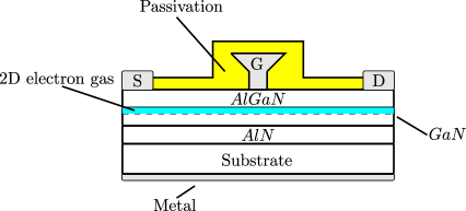
Figure 1 illustrates a basic GaN HEMT transistor structure. The transistor hetrostructure is placed on a substrate as discussed earlier in this article. An AlN buffer or nucleation layer is placed on the substrate after which a GaN layer is acting as the channel. An AlGaN barrier layer is deposited on top of the GaN layer forming a hetrojunction. The hetrojunction offers an important advantage as charge carriers are increased considerably without introducing dopant impurities and without degrading the mobility. This structure has the unique property in which charge carriers accumulate on the asymmetric junction formed between the two semiconductors with different band structures, confining them to the interface creating what is known as a two dimensional electron gas (2DEG). Transistors consisting of those structures are known as High Electron Mobility Transistors (HEMT) with GaN transistors, theoretically showing promise of cutoff frequencies up to the THz range. The important feature of nitrides is that they have a wurtzite crystal structure, which has a lower symmetry and hence built in polarization. In adition to this, when growing AlGaN on a GaN layer the AlGaN is stressed, creating piezoelectric polarization as it has a wider lattice structure than GaN. This adds to the spontaneous polarization built into the unstrained crystal resulting in a sheet of uncompensated positive charge at the interface creating a quantum well at the interface, leading to carrier confinement and a 2D electron gas in the undoped material as well as the doped one. This is in contrast to doped semiconductors such as GaAs and InP in which the doping itself is responsible for ionized impurity scattering, reducing mobility. The 2D electron gas in GaN has a sheet charge density of the order of that is five times larger than a similar device using GaAs/AlGaAs. A detailed account including the band structure can be found in [15]. There are other challenges that are still being ironed out with the GaN HEMT, resulting for example from surface stages on the AlGaN and traps near the interface in the GaN layer. Those things affect the mobility or create a virtual gate and are addressed structurally in various ways. For example, the passivation layer is intended to resolve the AlGaN surface states. There is an ongoing research focused on improvement of the crystalline layer purity and fabrication processes for reducing the density of the AlGaN buffer traps.
At this point, it is the time to place a distinction between small signal HEMTs which are important for this current discussion to HEMTs used in high frequency power switching. Current small signal devices begin at frequencies above , while most of the available work discusses power devices with larger gate lengths ( ) and larger device cross sections with lower cutoff frequencies. The higher breakdown voltage of the GaN (table 1) contributes to even smaller devices and gate sizes improving performance at high frequencies.
3.1 Operating frequency
High capacitance and low impedance are directly correlated to the transistors operating frequency. Increasing the cross section of the device, results in an increase in its capacitance as the capacitance is proportional to the area of the conductors, and at the same time reduces the impedance for the current increases (). Thus for our purposes two frequencies characterize the device the gain bandwidth product (GBP) the maximum frequency of oscillation
| (1) | ||||
| (2) |
where is the transconductance, the capacitive coupling between the gate and channel, a resistance modeling the drain source current, and the gate resistance. The GBP is the frequency in which is the short circuit current gain falls to unity while is the frequency in which the power gain falls to unity. The higher those values are the higher performance the device provides at higher frequencies. If the area of the device is larger it would increase the gate source capacitance reducing the GBP (equation 1). This in turn will affect the maximum frequency (equation 2), which would reduce that depends on the device area as well. Thus reducing the dimensions inherently increases the operating frequencies. One property of the material that affects the frequencies is the dielectric constant, as
a lower dielectric constant results in lower capacitive loading, thus increasing the operating frequency. Table 2 compares the dielectric constant of several semiconducting materials
| Material | [12] |
|---|---|
| GaAs | 12.5 |
| InP | 12.4 |
| Si | 11.9 |
| SiC | 10.0 |
| GaN | 9.5 |
| Diamond | 5.5 |
As can be seen, in this sense, GaN is favorable to other semiconducting materials excluding diamond. One has to recall that once we discuss the GaN HEMTs, the gate consists of a Shockley diode further reducing the gate channel capacitive coupling. Returning to table 1, it can be seen that both electron mobility and electron saturation velocity are higher in GaN than in SiC and Si, positioning it as the better material for high frequency solid state devices. To this we can add the polarized HEMT structure which is currently commercially unique to GaN providing much higher mobility compared to other materials including GaAs with a similar structure. It has a wider bandgap compared to GaAs which improves its reliability in environments with energetic radiation and a considerably lower noise figure [5], placing it in an attractive replacement in the first stage of the preamplifier. Here we have to state again, that we are interested that the device will obtain the higher frequency and not high frequency power devices for which the SiC may in certain circumstances be the better material due to its superior thermal conductivity.
In order to get some idea of the frequencies involved, some recent work should be referenced. Kabouche et. al. have reported an AlN/GaN HEMT with a maximum frequency [6], with Li et. al reporting a cutoff frequency, GBP of and maximum device frequency of [10]. This follows the work done by Y. Durmus obtaining GBP of and using AlGaN/GaN. While this displays frequencies nearing the THz range, available commercial devices which are designed mostly for power amplification, are available for cutoff frequencies of up to 20 GHz such as work from Kim et. al. with devices attaining GBP of approximately and of [8].
4 GaN HEMT and silicon JFET detection circuits (Preamplifiers)
The conventional way of sensing the -ray energy consists of using a JFET transistor (2N4416) as a source follower at the first stage tracing the voltage of the charge generated by the interaction with the photon and the detector. JFET’s are used due to their speed, low noise and high input impedance. A simple detection circuit, based on [18] is illustrated in figure 2.
In the above circuit, the HV bias controls the sensitivity of the circuit at times requiring the use of a second amplification stage consisting of the 2N3904 transistor. While the first stage transistor has a switching speed of , the actual measured time resolution at its output is approximately . The switching speed of the second general small signal amplifying transistor, is approximately providing a larger signal (small signal amplification) at the expense of the time resolution. This is followed by an amplifier with the provisions of shaping the signal obtained from the pre-amplifier. For pulse height spectroscopy an A/D and a multichannel analyzer are connected to the output. As we have seen earlier in this article, GaN based transistors are faster, thus replacing both stages with GaN transistors, one can expect that the time resolution would improve considerably. Having a wide bandgap GaN based transistors tend to be radiation hardened compared to the above circuit, increasing its reliability in environments where such radiation is abundant, such as space. Placing a GaN based FET at the first preamplification stage is attractive as it may not require the radiation shielding associated with shallow bandgap semiconductors, thus resulting in a reliable and compact circuit.
4.1 Preamplifier simulations
Prior to realizing a GaN circuit, its merits should be analyzed and different circuits including a GaN model need to be compared. The simulation was carried using LTspice XVII with a spice model of the fastest GaN HEMT that Efficient Power Conversion offers commercially [2]. Three circuits were compared, a preamplifier with a JFET input and bipolar transistor at its output (Figure 2), a preamplifier with a JFET at its input and an NMOS at its output and a circuit with an eGaN. The following simulations are for comparing theoretical features only. This will be followed by the measured output of practical circuits compared with the simulated result based on the measurement systems constraints. One has to remember, that we are testing the response of the system to a short pulse and in the following instances the simulated input pulses are large, driving the circuit into saturation, rendering the second stage as redundant, seemingly reducing the voltage amplification. In practice most of the pulses will have a much lower amplitude requiring the additional amplification. There will be instances in which using only the first stage will have its benefits especially when a response to very short pulses are a concern.
4.1.1 JFET input and bipolar transistor at the output
Figure 3 displays the circuit simulated of a preamplifier circuit with a JFET at the input (2N4416) and a generic bipolar transistor at the output (2N3904). The input stage consists of a high impedance source follower further amplified by the generic transistor.
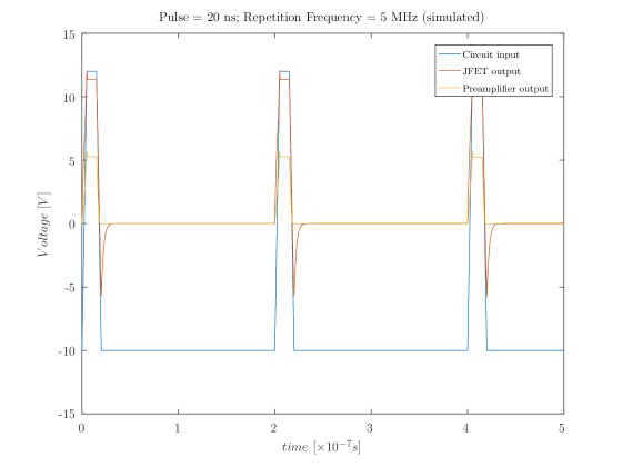
Instead of the detector we inserted a pulse generator with a pulse height of 20V, pulse width of 3ns and a period of 200ns. Figure 4 displays the simulation results of the pulse at the output of the JFET (J1) and the generic transistor (Q1).
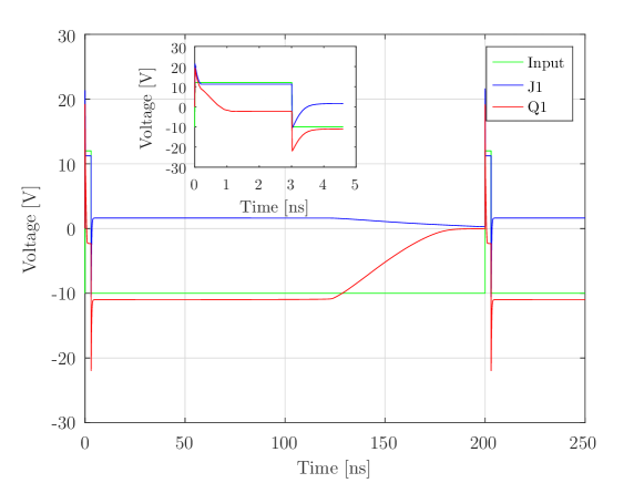
From the simulation it is obvious that the reverse recovery charge of the JFET and the resulting current , lead to spikes in the drain-source voltage. It is obvious as well that while the JFET’s response tracks the pulse fairly well, a residual voltage at the output results in Q1 conducting increasing the response time of the circuit to approximately . In the inset the response of both transistor outputs at the duration of the pulse are shown.
4.1.2 JFET input and NMOS output
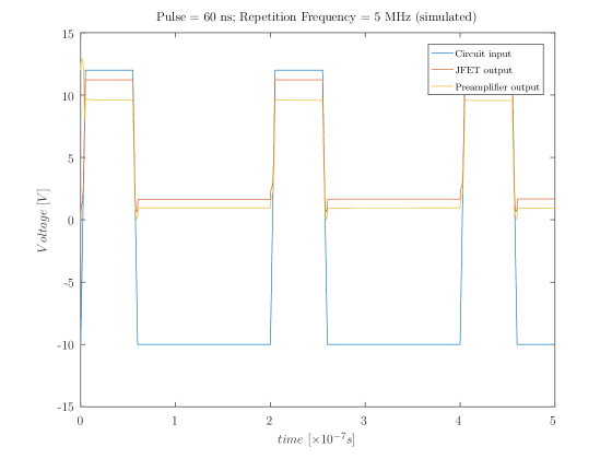
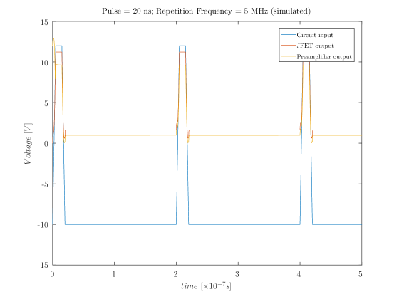
At this stage we wanted to test whether an improvement may be achieved using an NMOS at the ouput. Figure 5 illustrates the circuit used to simulate the preamplifier with the same JFET at the input but with a generic enhanced NMOS transistor at the output (2N7000). As the output consists of a source follower we do not expect a shift in the output.
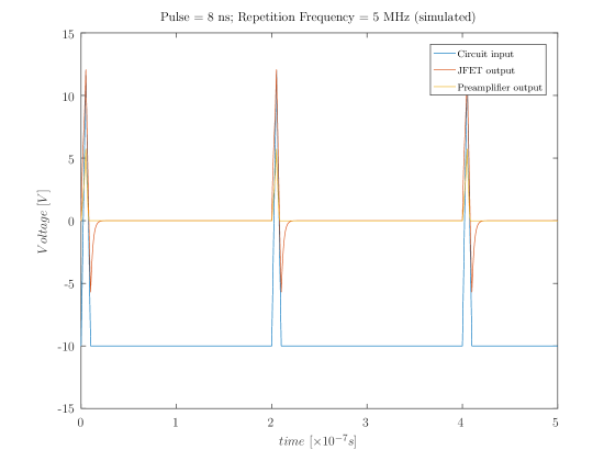
Once again, the circuit’s response was tested with a periodic short pulse, but as this circuit display a faster response the pulse width was reduced to with a period of . Figure 6 displays the resulting signals at the output of the JFET (J1) and the NMOS FET (M1).
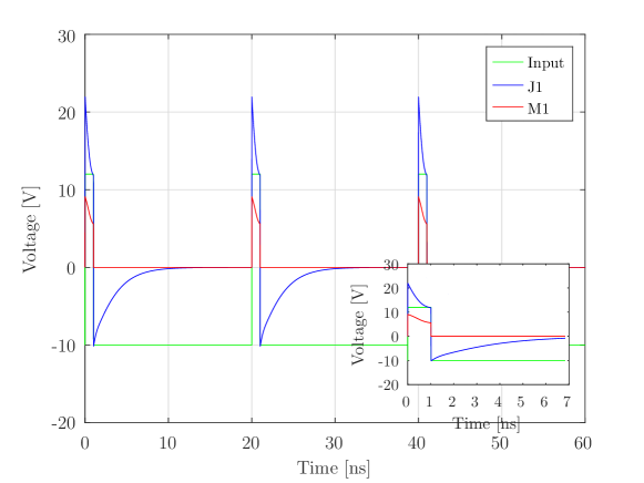
In this instance it is seen that the small signal NMOS FET does not display the negative voltage induced reverse recovery charge behavior while maintaining the width of the input pulse, though it does not completely track its form. It can be seen from Figure 6 that this has mostly to do with the JFET at the input.
4.1.3 GaN HEMT preamplifier
Figure 7 displays a preamplifier circuit based on a GaN transistor (EPC2038). The transistor is wired as a source follower.
This circuit is expected to display a faster response. The test signal consists of a 200ps wide pulse with a 1.5 ns period. Figure 8 displays the resulting signals at the output of the GaN HEMT (U1) and the NMOS FET (M1).
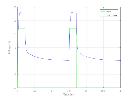
The simulation of this configuration shows a much better response tracking the input signal with an acceptable fidelity at the output.
4.2 Practical amplifier circuits
Once we have some understanding of the preamplifier circuit feasibility and expected response, we proceeded to realizing them as physical circuits. The circuits were an exact implementation of the simulated circuits excluding the GaN HEMT in which the second stage was omitted. An Agilent 33250 80MHz Function/Arbitrary waveform generator which can go all the way down to a pulse, was used as a test input signal for the various amplifiers. It was set to a repetition rate with and pulse widths. The pulses amplitude was rising from -10V to 10V. The generator features a minimum pulse width of 8ns and a minimum rise time of 5ns. Sampling was conducted using a Rohde Schartz RTM3004, 10Bit, 5GSa/s with a 1 GHz bandwidth. RT-ZP05, 10:1 ratio probes were used having a 500MHz bandwidth, impedance of and a typical rise time of 0.7 ns. Four points were sampled, at the input, at the output of the first amplifying stage, at the output of the second amplifying stage (with the DC bias) and at the preamplifiers output beyond the output capacitor. The following graphs for the various circuits illustrate their response to the generators pulse, given its minimum pulse width and rise time. The response of the physical circuit is compared to the simulated response cross validating both the circuits and the simulation.
4.2.1 JFET input with a bipolar transistor at the output
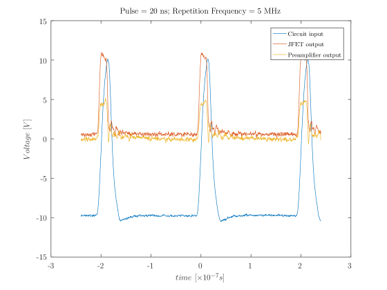
We begin by demonstrating measurements regarding the circuit with the JFET at its input stage (Figure 3). At the second stage we used a standard general 2N3904 NPN transistor. At the input stage we used a mil-spec 2N4416 N-Channel JFET in a TO206AF hermetically-sealed package. This is an important feature which will be discussed during stress testing in a following article. Figures (9-11) illustrate the measured response of the preamplifier to a repetitive pattern pulses of and given the generator limitations discussed above.
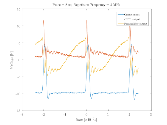
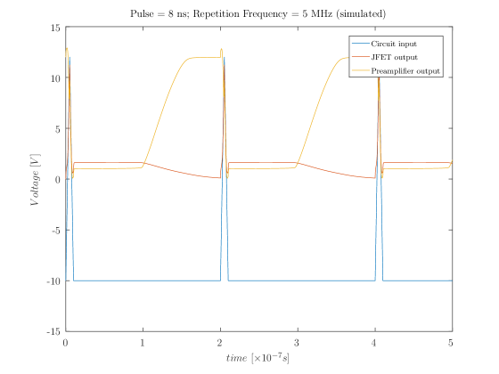
In all of the circuits the fast rise time and tracking of the JFET at the first stage is evident. Compared to the rise time of the pulse generator its response is almost instantaneous. This does not apply to the general type transistor which is evident from the response to the input in both the physical implementation of the circuit and the simulation.
4.2.2 JFET input and NMOS output
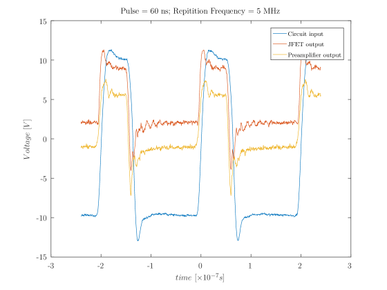
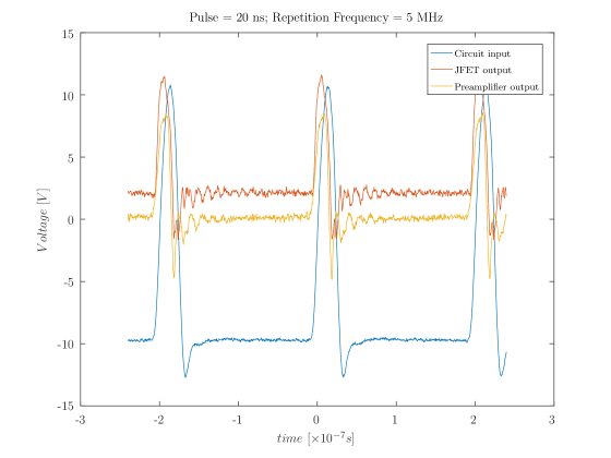
Next we test the 2N4416 JFET at the input with a standard 2N7000 NMOS at the output. Figures (12-14) illustrate the measured response of the preamplifier to a repetitive pulses of 60, 20 and 8 ns.
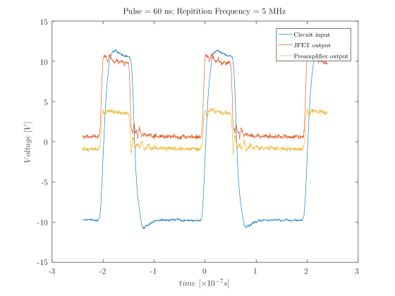
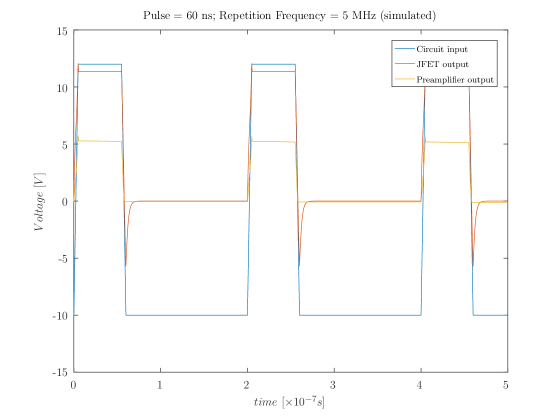
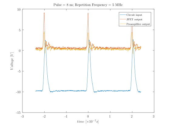
Once again the time response of the circuit in regards to the pulse is fast, displaying a faster response than the rise time of the generator. In this instance, the NMOS output tracks the JFET output without a noticeable delay at any of the pulse widths. This behavior is predicted by the simulation, deviating only on the account that the physical JFET does not display an overshoot when switched off. It can indicate that the actual JFET has either a much higher resistance, or a lower capacitance than the parameters given in the simulation.
4.2.3 GaN HEMT single stage
As this work lays the basis for the GaN HEMT as a hardened transistor in a preamplifier circuit, we tested it in a single stage configuration. In many circumstances this may suffice, providing as we shall see, a much faster response time with high sensitivity. The circuit was realized using an EPC2038 GaN HEMT. The response of the single stage GaN preamplifier is illustrated in figures (15-17). As the sensitivity of the GaN to the input is very strong we compared the rate of change of the voltage at the input and output, as it is obvious from the measured results that it is much faster at the output. We will refer to this rate of voltage change (maybe in an unorthodox manner) as the slew rate. In order to avoid cluttering the graphs and keeping them clear we opted to omit the output at the preamplifier (after the capacitor) and display only the measured output at the GaN transistor. The behavior at the output of the preamplifier, is similar to the behavior shown in the simulation.
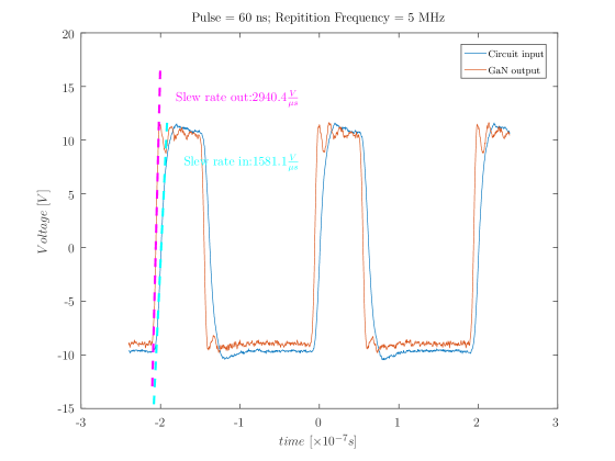
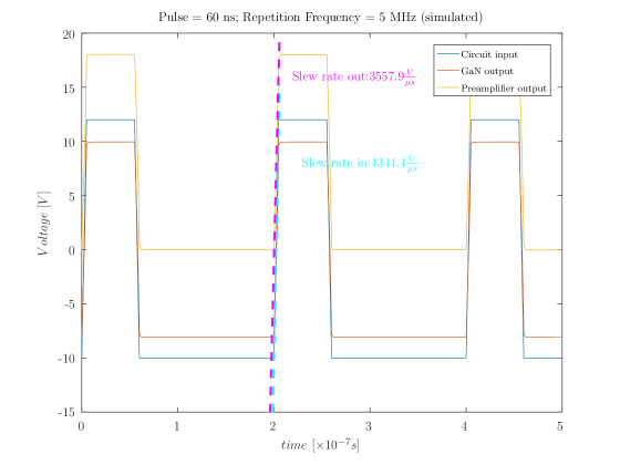
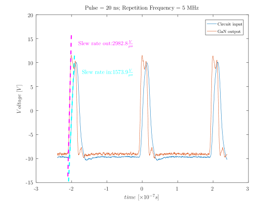
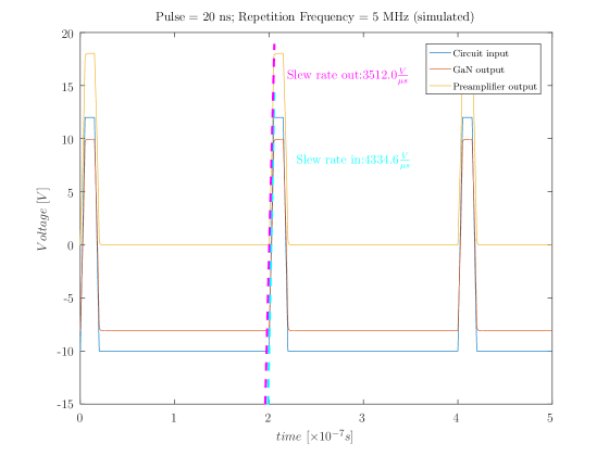
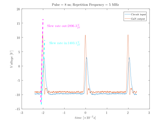
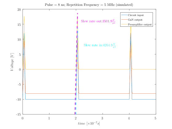
From the figures 15-17, it is obvious that in the real world the GaN’s slew rate is higher than the slew rate of the generator that we used. According to the displayed figures one can see that the GaN’s slew rate at is approximately double than that of the source at . On the other hand, looking at the simulated results, while we may say that the model approximates the GaN’s behavior with a slew rate of . It is obvious that the Frequency generator has less than half the specified slew rate of , thus in the experimental results it seems to lag behind the transistors.
5 Discussion
Having a Wide bandgap of , a critical field strength of and high electron mobility of places the GaN HEMPT as a very promising material for fast and hardened transistors required for radiation detectors. Further increasing its frequency performance, is creating a layered structure resulting in a high electron mobility transistor (HEMT). Such transistors are now commercially available, on both silicon and silicon carbide substrates mostly oriented to fast switching power applications. Our application is somewhat different as we intend to use the transistors for amplifying small signals in an environment with high energy particles and radiation, for which we need a radiation hardened and wide bandwidth preamplifier responding to short events, thus increasing our time resolution. The response of several preamplifier circuits were examined by both simulation and practical circuits. The first was a simple two stage amplifier with a wide bandwidth silicon JFET at the input and a bipolar transistor at the output. This was followed by a circuit consisting of a JFET at the input and a NMOS FET at the output. In a following simulation the input transistor was replaced by a GaN HEMT which is commercially available. The simulation results illustrate the superior performance of the GaN HEMT reliably amplifying pulses without much distortion down to pulse widths of 200 ps. As a whole we see the response of the physical circuits agreeing well with the simulations. Both the JFET input circuits and the GaN preamplifier display a fast response to the input displaying a much faster slew rate compared to the input signal. It was found that the actual slew rate of the GaN was approximately which is lower than that is predicted by the simulation. To our best knowledge no such comparative study was previously published.
This experimental work consists of some of the required underlying work for fabrication of preamplifiers for reliability testing while being exposed to radiation. Following this study, we will analyze the above circuits while being exposed to a source.
References
- [1] GI Ayzenshtat, VG Bozhkov, and A Yu Yushchenko. Measurement of the electron saturation velocity in an AlGaAs/InGaAs quantum well. Russian Physics Journal, 53(9), 2011.
- [2] Efficient Power Conversion. EPC2038 - Enhancement Mode Power Transistor, 2021.
- [3] Gady Golan, Moshe Azoulay, Tsuriel Avraham, Ilan Kremenetsky, and Joseph B Bernstein. An improved reliability model for Si and GaN power FET. Microelectronics Reliability, 81:77–89, 2018.
- [4] Gady Golan, Moshe Azoulay, Saleh Shaheen, and Joseph B Bernstein. A novel reliability model for GaN power FET. In 2018 IEEE International Conference on the Science of Electrical Engineering in Israel (ICSEE), pages 1–5. IEEE, 2018.
- [5] Christopher Harris, Raymond Pengelly, S Sheppard, T Smith, B Pribble, S Wood, and C Platis. Commercial gan devices for switching and low noise applications. In CS MANTECH Conference, 2011.
- [6] Riad Kabouche, Romain Pecheux, Kathia Harrouche, Etienne Okada, Farid Medjdoub, Joff Derluyn, Stefan Degroote, Marianne Germain, Filip Gucmann, Callum Middleton, et al. High efficiency aln/gan hemts for q-band applications with an improved thermal dissipation. International Journal of High Speed Electronics and Systems, 28(01n02):1940003, 2019.
- [7] Markus Kamp, C Kirchner, V Schwegler, A Pelzmann, Karl Joachim Ebeling, M Leszczynski, I Grzegory, T Suski, and S Porowski. GaN homoepitaxy for device applications. Materials Research Society Internet Journal of Nitride Semiconductor Research, 4(S1):878–889, 1999.
- [8] Hyun-Seop Kim, Myoung-Jin Kang, Jeong Jin Kim, Kwang-Seok Seo, and Ho-Young Cha. Effects of recessed-gate structure on algan/gan-on-sic mis-hemts with thin aloxny mis gate. Materials, 13(7):1538, 2020.
- [9] Masaaki Kuzuhara, Joel T Asubar, and Hirokuni Tokuda. AlGaN/GaN high-electron-mobility transistor technology for high-voltage and low-on-resistance operation. Japanese Journal of Applied Physics, 55(7):070101, 2016.
- [10] Lei Li, Kazuki Nomoto, Ming Pan, Wenshen Li, Austin Hickman, Jeffrey Miller, Kevin Lee, Zongyang Hu, Samuel James Bader, Soo Min Lee, et al. Gan hemts on si with regrown contacts and cutoff/maximum oscillation frequencies of 250/204 ghz. IEEE Electron Device Letters, 41(5):689–692, 2020.
- [11] PPG Microsemi. Gallium nitride (GaN) versus silicon carbide (SiC) in the high frequency (RF) and power switching applications. Digi-key, 2014.
- [12] Raymond S Pengelly, Simon M Wood, James W Milligan, Scott T Sheppard, and William L Pribble. A review of GaN on SiC high electron-mobility power transistors and MMICs. IEEE Transactions on Microwave Theory and Techniques, 60(6):1764–1783, 2012.
- [13] E. D. Pierron, D. L. Parker, and J. B. McNeely. Coefficient of expansion of GaAs, GaP, and Ga(As, P) compounds from to . Journal of Applied Physics, 38(12):4669–4671, 1967.
- [14] Fan Ren and John C Zolper. Wide energy bandgap electronic devices. World Scientific, 2003.
- [15] Fabrizio Roccaforte, Giuseppe Greco, Patrick Fiorenza, and Ferdinando Iucolano. An overview of normally-off GaN-based high electron mobility transistors. Materials, 12(10):1599, 2019.
- [16] D.F. Storm, M.T. Hardy, D.S. Katzer, N. Nepal, B.P. Downey, D.J. Meyer, Thomas O. McConkie, Lin Zhou, and David J. Smith. Critical issues for homoepitaxial gan growth by molecular beam epitaxy on hydride vapor-phase epitaxy-grown gan substrates. Journal of Crystal Growth, 456:121 – 132, 2016. Proceeding of the 9th International Workshop on Bulk Nitride Semiconductors.
- [17] Peter J Wellmann. Power electronic semiconductor materials for automotive and energy saving applications–SiC, GaN, , and diamond. Zeitschrift für anorganische und allgemeine Chemie, 643(21):1312–1322, 2017.
- [18] A Zuck, M Schieber, O Khakhan, H Gilboa, and Z Burshtein. Microstructure and energy resolution of 59.6 keV gamma absorption in polycrystalline detectors. IEEE Transactions on Nuclear Science, 51(3):1250–1255, 2004.