Electrical control of orbital and vibrational interlayer coupling in bi- and trilayer 2H-MoS2
Abstract
Manipulating electronic interlayer coupling in layered van der Waals (vdW) materials is essential for designing opto-electronic devices. Here, we control vibrational and electronic interlayer coupling in bi- and trilayer 2H-MoS2 using large external electric fields in a micro-capacitor device. The electric field lifts Raman selection rules and activates phonon modes in excellent agreement with ab-initio calculations. Through polarization resolved photoluminescence spectroscopy in the same device, we observe a strongly tunable valley dichroism with maximum circular polarization degree of in bilayer and in trilayer MoS2 that are fully consistent with a rate equation model which includes input from electronic band structure calculations. We identify the highly delocalized electron wave function between the layers close to the high symmetry points as the origin of the tunable circular dichroism. Our results demonstrate the possibility of electric field tunable interlayer coupling for controlling emergent spin-valley physics and hybridization driven effects in vdW materials and their heterostructures.
I Introduction
Breaking of crystal symmetries has profound effects on the electrical Zhang et al. (2009); Sui et al. (2015); Shimazaki et al. (2015) and optical properties Wu et al. (2013); Jones et al. (2014); Lee et al. (2016); Klein et al. (2016a) of vdW bonded materials and their heterostructures. A prime example is bilayer graphene, where an applied electric field breaks crystal inversion-symmetry that opens up a band gap Zhang et al. (2009) and induces, e.g., topological valley currents. Sui et al. (2015); Shimazaki et al. (2015) Monolayer transition-metal dichalcogenides (TMDCs), like MoS2, exhibit valley dichroism, due to their inherently broken inversion symmetry, where valleys are related to one another via time-reversal symmetry, as governed by the Kramer’s degeneracy. Mak et al. (2010); Splendiani et al. (2010); Mak et al. (2012); Zeng et al. (2012); Cao et al. (2012); Sallen et al. (2012) The 2H stacking results in alternating point groups with odd layer numbers manifesting in broken spatial inversion symmetry that is restored in either even layer crystals or evenly layered crystals. Several intriguing experimental observations, including electrical tuning of valley-magnetic moment Wu et al. (2013), spin-layer locking, Jones et al. (2014) and finite valley Hall effect, Lee et al. (2016) have been reported in bilayer TMDCs and ascribed to the control of Berry curvature, due to inversion symmetry breaking by an external electric field. Kormányos et al. (2018)
TMDCs exhibit a complex and intricate energy landscape in reciprocal space away from the points. Steinhoff et al. (2014, 2015, 2016) Other high symmetry points become relevant due to their momentum indirectness creating dark states that are experimentally not easily accessible, but contribute significantly to their optical and electronic properties. Wu et al. (2015); Qiu et al. (2015); Selig et al. (2016); Malic et al. (2018); Lindlau et al. (2018); Gerber et al. (2019); Paradisanos et al. (2020); Christiansen et al. (2019); Madéo et al. (2020) In this context, the point (also commonly denoted as or point) is of considerable importance due to the small energy difference between and in the conduction band. Steinhoff et al. (2014) Time-resolved -ARPES experiments have demonstrated that electrons can very effectively distribute between the and points Steinhoff et al. (2014, 2016) as experimentally observed in monolayer MoS2 Wallauer et al. (2016) and other TMDCs. Madéo et al. (2020) Furthermore, in multilayer TMDCs, the wave function overlap at the point is more pronounced due to the dominant sulfur -orbital admixture manifesting in efficient charge transfer, e.g., in heterobilayers. Wang et al. (2017); Jin et al. (2018); Kunstmann et al. (2018); Yuan et al. (2020); Ramzan et al. (2021)
In such multilayered systems, interlayer hopping of electrons or holes plays a crucial role for the formation of interlayer excitonic complexes. Miller et al. (2017); Wang et al. (2017); Jin et al. (2018); Gerber et al. (2019); Paradisanos et al. (2020); Leisgang et al. (2020); Lorchat et al. (2021) The re-distribution of charge carriers is realized by an ultra-fast charge transfer between the layers. Hong et al. (2014); Jin et al. (2018) Here, the application of an external electric field can control the layer hybridization Kiemle et al. (2020); Gao et al. (2017); Shimazaki et al. (2020); Leisgang et al. (2020) and tune hopping rates between individual layers to control photo-physical properties. Therefore, realizing field controlled multilayer devices made from TMDCs may offer novel device designs to control, e.g. spin-valley polarization for prospective opto-electronic devices.
In this Letter, we electrically control the interlayer hybridization in bi- and trilayer MoS2. From our measurements, we observe electric field-activated Raman modes, where the relative mode intensity is a fingerprint for the degree of interlayer (de)coupling. The observed activated phonon modes are in excellent agreement with - DFT calculated phonon spectra that include external electric fields. The phonon mode activation correlates with a highly tunable degree of circular polarization of the -exciton emission in inversion symmetric bilayer MoS2, with values varying with the electric field from up to , limited only by the maximally explored gate-voltage. Strikingly, the trilayer sample, which is intrinsically inversion symmetry broken, also reveals a tunable to , unlike the monolayer MoS2, where is field-independent. We interpret our observations in terms of the electric field dependent conduction and valence band edges at the / and / points. This changes the interlayer hybridization, most importantly for our experiments the electron wave function distribution between the layers at the / points results in an electric field dependent population of optically excited electrons and holes in the layers at the / points. We support our observations with a rate-equation model that takes into account the - calculated electronic band structure. Our results show that the points significantly influence electron hopping in 2H-multilayered TMDC crystals, and that the concept of symmetry alone is insufficient to explain optical dichroism in few-layer MoS2 but that interlayer coupling and in particular, the hopping of electrons strongly influences the redistribution of optically excited carriers in the multilayer sample. Our results further demonstrate the potential to control emergent spin- and valleytronic devices based on two-dimensional (2D) atomically thin crystals with electric fields.
II Results and Discussion
II.1 Microcapacitor device
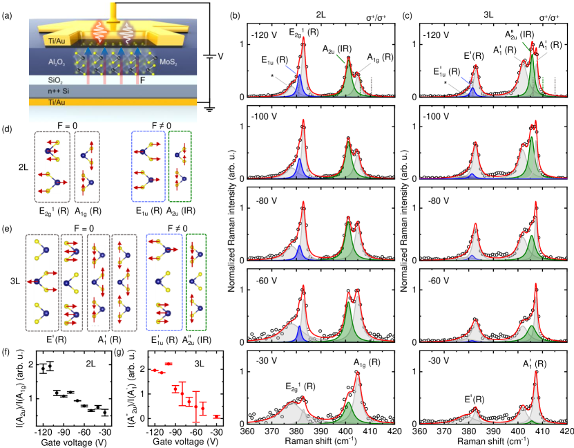
The investigated device consists of mono-, bi- and trilayer 2H-MoS2 embedded in a micro-capacitor structure. The layers are electrically isolated from the contacts, as depicted schematically in Fig. 1(a). A thick semi-transparent titanium top gate facilitates optical access to the crystals while applying a gate-voltage in the range of results in electric fields on the order of . Klein et al. (2016b, a) Raman and PL data are acquired keeping the device at a lattice temperature of and optically exciting at an energy of .
II.2 Activation of Raman modes by crystal symmetry breaking
The lattice vibrational modes in 2D materials encode rich information of crystal symmetries that can be directly derived from group theory. Verble and Wieting (1970); Molina-Sánchez and Wirtz (2011) The irreducible representation of a monolayer MoS2 ( point group) is with representing the in-plane (LA/TA) and out-of-plane (ZA) acoustic phonon modes, the IR active mode, and the Raman active modes, and representing an IR and Raman active mode. Zhao et al. (2013) Both, and Raman modes are active in our backscattering geometry. In order to study the effect of perturbing crystal symmetry using an out-of-plane electric field, we now tune the gate-voltage and study phonon modes.
| Mode | () | () | |
| 2L | |||
| 3L | |||
Gate-voltage dependent data for bi- and trilayer MoS2 are presented in Fig. 1(b) and (c). For maximally broken inversion symmetry in the bilayer and also in the trilayer ( in our device) additional phonon modes (colored blue and green) appear in the spectrum (see Fig. 1(b) and (c)). Their intensity monotonically decreases with decreasing gate-voltage.
To understand the origin of the field-activated phonon modes, we perform - DFT calculations of phonon spectra for mono-, bi- and trilayer MoS2 with and without electric field (see full phonon dispersion in the Supplemental Material). Our calculations indeed suggest additional electric-field-activated phonon modes, (R) ( (R)) and (IR) ( (IR)) in the bilayer (trilayer), due to the lifting of Raman selection rules. Corresponding atomic displacements are shown in Fig. 1(d) and (e). The experimental and theoretical values of phonon modes of bi- and trilayer are summarized in Tab. 1 and highlighted in the Raman spectra in Fig. 1(b) and (c). The calculated absolute phonon mode energies and their frequency differences are in excellent agreement with our experimental spectra. To quantify the extent to which symmetry is broken by the external electric field, we plot the ratio of phonon mode intensities between the and modes for the bilayer MoS2 and and modes for the trilayer MoS2 (see Fig. 1(f) and (g)). As expected, the highest ratio (degree of symmetry breaking) is observed for the maximum gate-voltage (electric field) while the ratio vanishes for decreasing gate-voltages . The offset from originates from the asymmetric dielectric environment and built-in electric field of the device as discussed in detail in Refs. Klein et al. (2016b, a). Note that we focus our discussion on positive gate-voltages since the total Raman intensity strongly diminishes at negative voltages due to carrier doping effects in the asymmetric device structure, Miller et al. (2019) which originate from charge transfer for this field polarity from the Al2O3 interface into the MoS2. Klein et al. (2016b, a) We can conclude that the appearance of new Raman modes for an applied electric field is a direct fingerprint for the change in vibrational coupling in our tunable micro-capacitor device.
II.3 Electrical control of interlayer hybridization
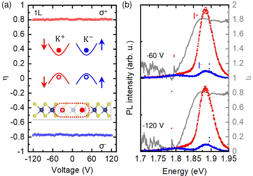
We now directly correlate the observed crystal symmetry breaking from our Raman measurements with circularly-polarized -PL of 1L, 2L and 3L MoS2. All measurements are performed with quasi-resonant excitation of the -exciton using a CW HeNe laser emitting at and the samples at a lattice temperature of . Polarization resolved PL spectra are recorded with (and ) polarized excitation and the emitted PL is analyzed with and discrimination. Both sets of data are equivalent since the and valleys are equivalent. The resulting PL spectra are denoted , where the superscript denotes the helicity of the polarization discrimination in the detection channel and is the energy of the emitted photons.
Typical gate-voltage dependent degree of valley polarization and the corresponding spectra recorded at and are shown in Fig. 2. We observe the direct gap -exciton transition in all spectra at . The degree of circular polarization is derived from the PL and spectra that is defined by and plotted in addition to the PL spectra in Fig. 2(b). The PL in monolayer MoS2 is strongly circularly polarized with . In general, is a measure for the optically excited steady-state carrier populations in the and valleys (schematically shown in Fig. 2(a)) reflecting the interplay between the interband optical selection rules, as well as intra- and intervalley relaxation dynamics that occur due to thermalization, and radiative recombination lifetimes. Palummo et al. (2015); Robert et al. (2016) For the monolayer, we observe a field-independent , which is a direct consequence of the inherently broken inversion symmetry and field-independent intervalley scattering. Wu et al. (2013) As evident from the data, for monolayer MoS2 is constant throughout the whole range of applied gate-voltages with a high value of in good agreement with previous reports. Mak et al. (2012); Zeng et al. (2012); Wu et al. (2013); Kioseoglou et al. (2012)
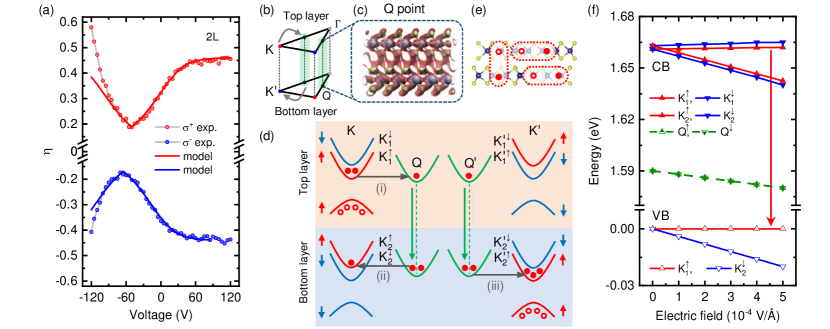
Unlike the monolayer, the inversion symmetric bilayer shows a strongly tunable (see Fig. 3(a)). Here, we observe the lowest for where crystal symmetry is maximally restored in our asymmetric device in very good agreement with the absence of field-activated Raman modes (see Fig. 1(b)). In contrast, for , symmetry is maximally broken in our device for which we also observe the field-activated Raman modes with highest intensity. This observation clearly reflects the lifted crystal inversion symmetry, and therefore change in the electronic interlayer coupling directly affecting the degree of valley polarization in the bilayer.
Considering the weak interlayer coupling in TMDCs, relaxation dynamics are expected to significantly depend on the hybridization of sulfur -orbitals between proximal layers in MoS2. While the conduction bands at / show only a weak admixture of the sulfur -orbitals since they are mainly comprised of Mo -orbitals, the points have a predominant contribution from the -orbitals. Liu et al. (2013) The relevant high symmetry points in momentum space of the coupled bilayer system are schematically depicted in Fig. 3(b). The points strongly connect the top and bottom layer, which is also directly apparent from the strong delocalization of our DFT-computed wave function at the point (see Fig. 3(c)). Note that holes in multilayer MoS2 also show a delocalization between points, Gong et al. (2013); Deilmann and Thygesen (2018); Slobodeniuk et al. (2019); Guo et al. (2018); Hsu et al. (2019); Leisgang et al. (2020) however, this delocalization is much weaker as compared to the strong delocalization of electrons in the CB at (see Supplemental Material for additional wave function calculations at the point).
Our experiments show that even when the excitation is circularly polarized and resonant with the -exciton, a fraction (percentage ) of light is emitted with opposite helicity (at ). This recombination channel implies an intervalley scattering of carriers that is independent of the applied gate-voltage and should be also present in multilayered structures. The variation of as function of the gate-voltage is an effect that can only be observed in multilayered systems and is the result of an interplay between the realignment of the hybridized bands and transfer of photoexcited carriers through different layers.
To explain the degree of polarization in the PL emission of multilayered systems, we consider only the excitation and a voltage (electric field) that pushes the electrons from the top layer to the bottom layer (see Fig. 3(d)). Since this model is symmetric, electric fields in the opposite directions and excitation are equivalent. The quasi-resonant excitation of a bilayer MoS2 generates a steady-state electronic distribution in the CB with electrons residing in the , , and valleys (Fig. 3(d)). Steinhoff et al. (2014, 2015, 2016); Wallauer et al. (2016); Madéo et al. (2020) As we consider only the scattering of electrons from to valley and from to valley, we analyze each case separately. Considering that we excited electrons in each case, a fraction of them reside in the valley of the top layer, while are in the valley, distributed through both layers (see dotted lines Fig. 3(d)). Without a gate-voltage applied, the differential rate equations that describe the dynamics of these two levels are
| (1) |
and
| (2) |
where is the electronic population in the state and its time derivative. is the radiative recombination lifetime and, and are the lifetime for non-radiative recombination channels in each valley, and , respectively.
The application of a gate-voltage generates additional transitions that modify the steady-state and consequently the polarization of the photoluminescence. These transitions are labeled as (i) and (ii) in Fig. 3(d) for the to scattering case. The green arrows represent the polarization of the valley that facilitates the transfer of electrons to the bottom layer. This is the central effect in this model affecting the circular polarization degree for all multilayer samples. The redistribution of electrons via the point manifests in the formation of intra- and interlayer excitons in the bilayer (see Fig 3(e)). The field-dependent first principle calculations and corresponding energy shifts of the and points in Fig. 3(f) show, as the most important effect, a strong reduction of the energy distance between the point and the valley. This enhances transition (ii) at the same time that transition (i) appears to have, in comparison, a reduced contribution. On the other hand, the outstanding effect of the gate-voltage is the population increase of electrons in bright states ( point) at the expense of dark states ( valley) and this effect can be well described by subtracting from the valley rate equation. Here, accounts for the tuneability of the system with gate-voltage , and represents the lifetime for transition (ii). This term constitutes in a source term for the latter level, whose complete rate equation is
| (3) |
We model the function as an exponential growth
| (4) |
whose value is identically zero for and is a fitting parameter. It is important to note that the interlayer exciton in MoS2 is the result of a strong admixture between a intralayer exciton and an interlayer exciton. Leisgang et al. (2020); Gerber et al. (2019); Deilmann and Thygesen (2018) In our case, we do not consider this situation because the laser energy used in the experiments does not allow for the formation of excitons. Holes are strongly localized in the top layer and the recombination process from the level would describe the annihilation of interlayer excitons with radiative and non-radiative lifetimes of and , respectively.
In the scattering from and case, the excitation with light generates spin-up electrons in of the bilayer and of the bottom layer with similar dynamics as in the and points. Including the gate-voltage effect which activates the transition labeled (iii) in Fig. 3(d), their rate equations are
| (5) |
and
| (6) |
Since both layers are equivalent, the radiative and non-radiative lifetimes involved in the process are the same. In addition, and are also equivalent points of the bilayer with the same non-radiative lifetime.
All the radiative transitions described in the rate equations above correspond to light emitted with polarization. The intervalley scattering, , yields polarized light. By solving these equations in the steady-state with realistic material parameters, we determine the polarized emission intensity and calculate the circular polarization degree of the PL using , and as fitting parameters. Note that this emission originates from both, intra- and interlayer excitons (see Fig. 3(e)). The total emission is then the sum of both processes. The calculated electric field dependent circular polarization degree is presented in Fig. 3(a), showing excellent agreement with the experiment. Both data sets are fitted individually due to a small difference in the voltage offset that originates from the subsequent recording of data and the hysteresis of the device. Klein et al. (2016b) The corresponding material and fitting parameters are listed in the Supplemental Material.
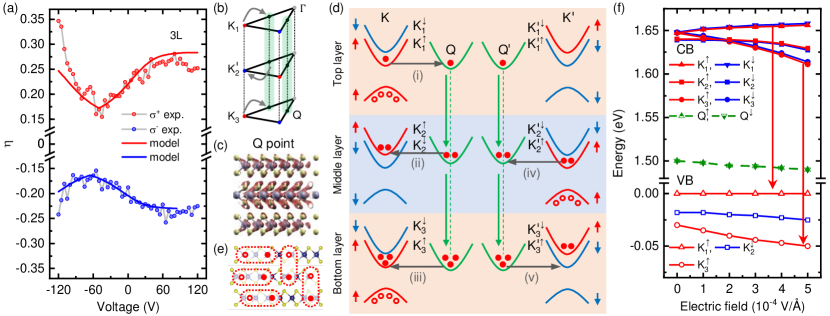
Since our model stems from steady-state electron distributions, similar dependencies of are expected for systems with more than two layers. Indeed, probing the trilayer MoS2, we obtain a similar modulation of as shown in Fig. 4(a). For the case where the symmetry between the layers is restored (), we obtain a minimum while for the highest electric-field () a maximum is observed. Similar to the bilayer case, we find a strong delocalization of the electron wave function at the points (see Fig. 4(b) and (c)) suggesting a similar steady-state population redistribution of electrons throughout the trilayer. The level scheme for a trilayer is analogous to the bilayer by adding an additional layer as shown in Fig. 4(d). Similar to the bilayer, it allows the formation of intra- and interlayer excitons (see Fig. 4(e)). The computed CB and VB edges of / and / points are shown in Fig. 4(f). For a finite field of , the energy sequence in the CB and VB follow the stacking order of the layers resulting in a field-dependent electron distribution throughout the trilayer that is mediated via the point (see Fig. 4(d) and (f)). We solved the rate equation model for a trilayer system (see Fig. 4(d)) analogously to the bilayer. The resulting is again in excellent agreement with experimental data (see Fig. 4(a)).
The valley optical selection rules in TMDCs are strongly connected to the crystal inversion symmetry and time-reversal symmetry (Kramer’s degeneracy). 2H trilayer TMDCs are intrinsically inversion symmetry broken and therefore, tuneability of the optical valley dichroism is not expected. This results for example in a non-tunable second-harmonic generation. Klein et al. (2016a) However, our observation of field-tunable in the trilayer suggests that the breaking of the Kramer’s degeneracy and the accompanying occurrence of a valley magnetic moment Wu et al. (2013) is not sufficient to explain our data (see Fig. 4(a)). Our results and microscopic modeling based on DFT calculation input suggest that the high-symmetry point and a field-dependent change in the interlayer hybridization, and therefore interlayer hopping can strongly modify the steady-state electron, and therefore exciton population in the bi- and trilayer system manifesting in the tunable valley dichroism. This is in contrast to earlier work that attributed it solely to a change in the valley magnetic moment. Wu et al. (2013); Kormányos et al. (2018)
III Conclusion
In summary, we demonstrated the electrical control of interlayer vibrational and orbital coupling in bi- and trilayer MoS2. Field-dependent Raman spectroscopy is a useful tool to probe the symmetry and layer decoupling of bi- and trilayer crystals. Our work suggests that the point in multilayer TMDCs is important for understanding steady-state electron populations and, therefore, the spin-valley dichroism of TMDCs and other vdW heterostructures.
IV Acknowledgements
We gratefully acknowledge financial support from ExQM PhD programme of the Elite Network of Bavaria, the German Excellence Initiative via the Nanosystems Initiative Munich (NIM), the Deutsche Forschungsgemeinschaft (DFG) via the clusters of excellence e-conversion (EXC 2111) and MCQST (EXC 2089), via SPP 2244, the European Union’s Horizon 2020 research and innovation programme under grant agreement No. 820423 (S2QUIP) and through the TUM International Graduate School of Science and Engineering (IGSSE). J.K. acknowledges support by the Alexander von Humboldt foundation.
A.K. acknowledges DFG project GRK 2247/1 (QM3), and the association with SPP 2244. A.K. and T.B. acknowledge the support by the DFG within SFB 1415 and the high-performance computing center of ZIH Dresden for computational resources. We further thank Ursula Wurstbauer and Andor Kormányos for insightful and stimulating discussions.
V Author contributions
J.K., J.W., K.M. and J.J.F. conceived and designed the experiments, J.K. and J.W. prepared the samples, J.K. and J.W. performed the optical measurements, J.K. analyzed the data, P.S., J.K. and A.V.S. developed the rate equation model, A.K. and L.M. computed the electric field-dependent Raman and phonon-dispersion spectra, T.B. computed the field-dependent electronic band structures, J.K. wrote the paper with input from all co-authors. All authors reviewed the manuscript.
VI Methods
VI.1 Device fabrication
The MoS2 crystal is mechanically exfoliated onto a thick SiO2 layer on a heavily n-doped silicon substrate. Spatially resolved Raman spectroscopy and white light interferometry are used to identify mono-, bi- and trilayer regions of the flake, before it is capped with a thick Al2O3 dielectric using atomic layer deposition (ALD) at a low temperature of . An electrical contact is established to the silicon substrate and the sample is completed with a thick semi-transparent titanium top contact that facilitates optical access to the crystal while tuning the gate-voltage (electric field) in the range . The device fabrication procedure is found to have no significant deleterious impact on the photoluminescence properties of the atomically thin flake. Further details of the fabrication, electrical characterization and control of the -exciton emission energies using the DC-Stark effect and control of second-harmonic generation (SHG) can be found in Ref. Klein et al. (2016b) and Ref. Klein et al. (2016a).
VI.2 Optical spectroscopy
For low-temperature confocal -PL and Raman measurements we keep the device under vacuum in a helium flow cryostat with a lattice temperature kept at . For circularly polarized measurements, we use a HeNe laser with an excitation energy of . An excitation power density of is used. The laser spot has a diameter of .
VI.3 DFT calculations
All materials (1L-3L MoS2) were fully optimized, including the lattice parameters and the atomic positions using density-functional theory with Perdew-Burke-Ernzerhof (PBE)Perdew et al. (1996) exchange-correlation functional together with D3 London dispersion correctionGrimme (2006) as implemented in Crystal17.Dovesi et al. (2017, ) The resulting lattice parameters and are: 3.137 Å for 1L, 3.136 Å for 2L, and 3.135 Å for 3L, while interlayer distance between metal centers is Å. For Mo atoms, we used small-core effective-core pseudopotential (ECP) of the Hay–Wadt typeCora et al. (1997) which accounted for the electrons 1s2–3d10, while for S atoms, we used 86-311G∗.Lichanot et al. (1993) The 881 -point grid was used for structural relaxation. For Raman and phonon-dispersion calculations, geometries were re-optimized applying external electric field of a given strength perpendicular to the basal plane of the layers. Phonon dispersion calculations were performed using finite displacement method on the 551 supercells. Raman active modes were calculated at the -point.
Using the geometries as relaxed with Crystal17, the field-dependent electronic band structures and the corresponding spin projections have been calculated within the framework of DFT as implemented in the Quantum ESPRESSO package.Giannozzi et al. (2009, 2017) We employed full-relativistic, projector-augmented wave potentialsKresse and Joubert (1999) of the version 1.0.0 of the pslibraryCorso (2014); *pslib and we also chose the PBEPerdew et al. (1996) for the exchange-correlation energy. A cutoff of and () for the wave functions and the charge density, respectively, was used. The convergence was checked with higher cutoffs which lead to only slight shifts of the semi-core states at energies lower than below the Fermi energy. The Brillouin zone integration was performed with a -centered Monkhorst-Pack gridMonkhorst and Pack (1976) of -points together with a Gaussian broadening of . The self-consistent solution of the Kohn-Sham equations was obtained when the total energy changed by less than .
VI.4 Rate equation model
See Supplemental Material.
VII Abbreviations
Two-dimensional, 2D; TMDC, transition metal dichalcogenides; µ-PL, micro-photoluminescence; DFT, density functional theory; IR, infrared; Conduction band, CB; Valence band, VB;
VIII Additional information
VIII.1 Supplementary Information
Supplemental Material accompanies this paper.
VIII.2 Competing financial interests
The authors declare no competing financial interests.
References
- Zhang et al. (2009) Y. Zhang, T.-T. Tang, C. Girit, Z. Hao, M. C. Martin, A. Zettl, M. F. Crommie, Y. R. Shen, and F. Wang, Nature 459, 820 (2009).
- Sui et al. (2015) M. Sui, G. Chen, L. Ma, W.-Y. Shan, D. Tian, K. Watanabe, T. Taniguchi, X. Jin, W. Yao, D. Xiao, and Y. Zhang, Nat Phys 11, 1027 (2015), letter.
- Shimazaki et al. (2015) Y. Shimazaki, M. Yamamoto, I. V. Borzenets, K. Watanabe, T. Taniguchi, and S. Tarucha, Nat Phys 11, 1032 (2015), letter.
- Wu et al. (2013) S. Wu, J. S. Ross, G.-B. Liu, G. Aivazian, A. Jones, Z. Fei, W. Zhu, D. Xiao, W. Yao, D. Cobden, and X. Xu, Nature Physics 9, 149 (2013).
- Jones et al. (2014) A. M. Jones, H. Yu, J. S. Ross, P. Klement, N. J. Ghimire, J. Yan, D. G. Mandrus, W. Yao, and X. Xu, Nat Phys 10, 130 (2014), letter.
- Lee et al. (2016) J. Lee, K. F. Mak, and J. Shan, Nat Nano 11, 421 (2016), letter.
- Klein et al. (2016a) J. Klein, J. Wierzbowski, A. Steinhoff, M. Florian, M. Rösner, F. Heimbach, K. Müller, F. Jahnke, T. O. Wehling, J. J. Finley, and M. Kaniber, Nano Letters 17, 392 (2016a).
- Mak et al. (2010) K. F. Mak, C. Lee, J. Hone, J. Shan, and T. F. Heinz, Phys. Rev. Lett. 105, 136805 (2010).
- Splendiani et al. (2010) A. Splendiani, L. Sun, Y. Zhang, T. Li, J. Kim, C.-Y. Chim, G. Galli, and F. Wang, Nano letters 10, 1271 (2010).
- Mak et al. (2012) K. F. Mak, K. He, J. Shan, and T. F. Heinz, Nat Nano 7, 494 (2012).
- Zeng et al. (2012) H. Zeng, J. Dai, W. Yao, D. Xiao, and X. Cui, Nat Nano 7, 490 (2012).
- Cao et al. (2012) T. Cao, G. Wang, W. Han, H. Ye, C. Zhu, J. Shi, Q. Niu, P. Tan, E. Wang, B. Liu, and J. Feng, 3, 887 EP (2012), article.
- Sallen et al. (2012) G. Sallen, L. Bouet, X. Marie, G. Wang, C. R. Zhu, W. P. Han, Y. Lu, P. H. Tan, T. Amand, B. L. Liu, and B. Urbaszek, Phys. Rev. B 86, 081301 (2012).
- Kormányos et al. (2018) A. Kormányos, V. Zólyomi, V. I. Falko, and G. Burkard, Physical Review B 98 (2018), 10.1103/physrevb.98.035408.
- Steinhoff et al. (2014) A. Steinhoff, M. Rösner, F. Jahnke, T. O. Wehling, and C. Gies, Nano Letters 14, 3743 (2014).
- Steinhoff et al. (2015) A. Steinhoff, J.-H. Kim, F. Jahnke, M. Rosner, D.-S. Kim, C. Lee, G. H. Han, M. S. Jeong, T. Wehling, and C. Gies, Nano letters 15, 6841 (2015).
- Steinhoff et al. (2016) A. Steinhoff, M. Florian, M. Rösner, M. Lorke, T. O. Wehling, C. Gies, and F. Jahnke, 2D Materials 3, 031006 (2016).
- Wu et al. (2015) F. Wu, F. Qu, and A. H. MacDonald, Physical Review B 91 (2015), 10.1103/physrevb.91.075310.
- Qiu et al. (2015) D. Y. Qiu, T. Cao, and S. G. Louie, Physical Review Letters 115 (2015), 10.1103/physrevlett.115.176801.
- Selig et al. (2016) M. Selig, G. Berghäuser, A. Raja, P. Nagler, C. Schüller, T. F. Heinz, T. Korn, A. Chernikov, E. Malic, and A. Knorr, Nature Communications 7 (2016), 10.1038/ncomms13279.
- Malic et al. (2018) E. Malic, M. Selig, M. Feierabend, S. Brem, D. Christiansen, F. Wendler, A. Knorr, and G. Berghäuser, Physical Review Materials 2 (2018), 10.1103/physrevmaterials.2.014002.
- Lindlau et al. (2018) J. Lindlau, M. Selig, A. Neumann, L. Colombier, J. Förste, V. Funk, M. Förg, J. Kim, G. Berghäuser, T. Taniguchi, K. Watanabe, F. Wang, E. Malic, and A. Högele, Nature Communications 9 (2018), 10.1038/s41467-018-04877-3.
- Gerber et al. (2019) I. C. Gerber, E. Courtade, S. Shree, C. Robert, T. Taniguchi, K. Watanabe, A. Balocchi, P. Renucci, D. Lagarde, X. Marie, and B. Urbaszek, Physical Review B 99 (2019), 10.1103/physrevb.99.035443.
- Paradisanos et al. (2020) I. Paradisanos, S. Shree, A. George, N. Leisgang, C. Robert, K. Watanabe, T. Taniguchi, R. J. Warburton, A. Turchanin, X. Marie, I. C. Gerber, and B. Urbaszek, Nature Communications 11 (2020), 10.1038/s41467-020-16023-z.
- Christiansen et al. (2019) D. Christiansen, M. Selig, E. Malic, R. Ernstorfer, and A. Knorr, Physical Review B 100 (2019), 10.1103/physrevb.100.205401.
- Madéo et al. (2020) J. Madéo, M. K. L. Man, C. Sahoo, M. Campbell, V. Pareek, E. L. Wong, A. Al-Mahboob, N. S. Chan, A. Karmakar, B. M. K. Mariserla, X. Li, T. F. Heinz, T. Cao, and K. M. Dani, Science 370, 1199 (2020).
- Wallauer et al. (2016) R. Wallauer, J. Reimann, N. Armbrust, J. Güdde, and U. Höfer, Applied Physics Letters 109, 162102 (2016).
- Wang et al. (2017) Y. Wang, Z. Wang, W. Yao, G.-B. Liu, and H. Yu, Physical Review B 95 (2017), 10.1103/physrevb.95.115429.
- Jin et al. (2018) C. Jin, E. Y. Ma, O. Karni, E. C. Regan, F. Wang, and T. F. Heinz, Nature Nanotechnology 13, 994 (2018).
- Kunstmann et al. (2018) J. Kunstmann, F. Mooshammer, P. Nagler, A. Chaves, F. Stein, N. Paradiso, G. Plechinger, C. Strunk, C. SchÃŒller, G. Seifert, D. R. Reichman, and T. Korn, Nature Physics 14, 801 (2018).
- Yuan et al. (2020) L. Yuan, B. Zheng, J. Kunstmann, T. Brumme, A. B. Kuc, C. Ma, S. Deng, D. Blach, A. Pan, and L. Huang, Nature Materials 19, 617 (2020).
- Ramzan et al. (2021) M. S. Ramzan, J. Kunstmann, and A. B. Kuc, Small , 2008153 (2021).
- Miller et al. (2017) B. Miller, A. Steinhoff, B. Pano, J. Klein, F. Jahnke, A. Holleitner, and U. Wurstbauer, Nano Letters 17, 5229 (2017).
- Leisgang et al. (2020) N. Leisgang, S. Shree, I. Paradisanos, L. Sponfeldner, C. Robert, D. Lagarde, A. Balocchi, K. Watanabe, T. Taniguchi, X. Marie, R. J. Warburton, I. C. Gerber, and B. Urbaszek, Nature Nanotechnology (2020), 10.1038/s41565-020-0750-1.
- Lorchat et al. (2021) E. Lorchat, M. Selig, F. Katsch, K. Yumigeta, S. Tongay, A. Knorr, C. Schneider, and S. Höfling, Physical Review Letters 126 (2021), 10.1103/physrevlett.126.037401.
- Hong et al. (2014) X. Hong, J. Kim, S.-F. Shi, Y. Zhang, C. Jin, Y. Sun, S. Tongay, J. Wu, Y. Zhang, and F. Wang, Nature Nanotechnology 9, 682 (2014).
- Kiemle et al. (2020) J. Kiemle, F. Sigger, M. Lorke, B. Miller, K. Watanabe, T. Taniguchi, A. Holleitner, and U. Wurstbauer, Physical Review B 101 (2020), 10.1103/physrevb.101.121404.
- Gao et al. (2017) S. Gao, L. Yang, and C. D. Spataru, Nano Letters 17, 7809 (2017).
- Shimazaki et al. (2020) Y. Shimazaki, I. Schwartz, K. Watanabe, T. Taniguchi, M. Kroner, and A. Imamoğlu, Nature 580, 472 (2020).
- Klein et al. (2016b) J. Klein, J. Wierzbowski, A. Regler, J. Becker, F. Heimbach, K. Müller, M. Kaniber, and J. J. Finley, Nano Letters 16, 1554 (2016b).
- Verble and Wieting (1970) J. L. Verble and T. J. Wieting, Physical Review Letters 25, 362 (1970).
- Molina-Sánchez and Wirtz (2011) A. Molina-Sánchez and L. Wirtz, Physical Review B 84 (2011), 10.1103/physrevb.84.155413.
- Zhao et al. (2013) Y. Zhao, X. Luo, H. Li, J. Zhang, P. T. Araujo, C. K. Gan, J. Wu, H. Zhang, S. Y. Quek, M. S. Dresselhaus, and Q. Xiong, Nano Letters 13, 1007 (2013).
- Miller et al. (2019) B. Miller, J. Lindlau, M. Bommert, A. Neumann, H. Yamaguchi, A. Holleitner, A. Högele, and U. Wurstbauer, Nature Communications 10 (2019), 10.1038/s41467-019-08764-3.
- Palummo et al. (2015) M. Palummo, M. Bernardi, and J. C. Grossman, Nano Letters 15, 2794 (2015).
- Robert et al. (2016) C. Robert, D. Lagarde, F. Cadiz, G. Wang, B. Lassagne, T. Amand, A. Balocchi, P. Renucci, S. Tongay, B. Urbaszek, and X. Marie, Phys. Rev. B 93, 205423 (2016).
- Kioseoglou et al. (2012) G. Kioseoglou, A. T. Hanbicki, M. Currie, A. L. Friedman, D. Gunlycke, and B. T. Jonker, Applied Physics Letters 101, 221907 (2012), http://dx.doi.org/10.1063/1.4768299 .
- Liu et al. (2013) G.-B. Liu, W.-Y. Shan, Y. Yao, W. Yao, and D. Xiao, Physical Review B 88 (2013), 10.1103/physrevb.88.085433.
- Gong et al. (2013) Z. Gong, G.-B. Liu, H. Yu, D. Xiao, X. Cui, X. Xu, and W. Yao, 4, 2053 EP (2013), article.
- Deilmann and Thygesen (2018) T. Deilmann and K. S. Thygesen, Nano Letters 18, 2984 (2018).
- Slobodeniuk et al. (2019) A. O. Slobodeniuk, Ł. Bala, M. Koperski, M. R. Molas, P. Kossacki, K. Nogajewski, M. Bartos, K. Watanabe, T. Taniguchi, C. Faugeras, and M. Potemski, 2D Materials 6, 025026 (2019).
- Guo et al. (2018) L. Guo, M. Wu, T. Cao, D. M. Monahan, Y.-H. Lee, S. G. Louie, and G. R. Fleming, Nature Physics 15, 228 (2018).
- Hsu et al. (2019) W.-T. Hsu, B.-H. Lin, L.-S. Lu, M.-H. Lee, M.-W. Chu, L.-J. Li, W. Yao, W.-H. Chang, and C.-K. Shih, Science Advances 5, eaax7407 (2019).
- Perdew et al. (1996) J. P. Perdew, K. Burke, and M. Ernzerhof, Phys. Rev. Lett. 77, 3865 (1996).
- Grimme (2006) S. Grimme, J. Comp. Chem. 27, 1787 (2006).
- Dovesi et al. (2017) R. Dovesi, V. R. Saunders, C. Roetti, R. Orlando, C. M. Zicovich-Wilson, F. Pascale, B. Civalleri, K. Doll, N. M. Harrison, I. J. Bush, P. D’Arco, M. Llunell, M. Causá, Y. Noël, L. Maschio, A. Erba, M. Rerat, and S. Casassa, “Crystal17 user’s manual (university of torino, torino, 2017).” (CRYSTAL17 User’s Manual (University of Torino, Torino, 2017).).
- (57) R. Dovesi, A. Erba, R. Orlando, C. M. Zicovich-Wilson, B. Civalleri, L. Maschio, M. Rerat, S. Casassa, J. Baima, S. Salustro, and B. Kirtman, Wiley Interdiscip. Rev.: Comput. Mol. Sci. 8, e1360.
- Cora et al. (1997) F. Cora , A. Patel, N. M. Harrison, C. Roetti, and C. Richard A. Catlow, J. Mater. Chem. 7, 959 (1997).
- Lichanot et al. (1993) A. Lichanot, E. Aprà , and R. Dovesi, Physica Status Solidi (b) 177, 157 (1993).
- Giannozzi et al. (2009) P. Giannozzi, S. Baroni, N. Bonini, M. Calandra, R. Car, C. Cavazzoni, D. Ceresoli, G. L. Chiarotti, M. Cococcioni, I. Dabo, A. D. Corso, S. de Gironcoli, S. Fabris, G. Fratesi, R. Gebauer, U. Gerstmann, C. Gougoussis, A. Kokalj, M. Lazzeri, L. Martin-Samos, N. Marzari, F. Mauri, R. Mazzarello, S. Paolini, A. Pasquarello, L. Paulatto, C. Sbraccia, S. Scandolo, G. Sclauzero, A. P. Seitsonen, A. Smogunov, P. Umari, and R. M. Wentzcovitch, J. Phys.: Condens. Matter 21, 395502 (2009).
- Giannozzi et al. (2017) P. Giannozzi, O. Andreussi, T. Brumme, O. Bunau, M. B. Nardelli, M. Calandra, R. Car, C. Cavazzoni, D. Ceresoli, M. Cococcioni, N. Colonna, I. Carnimeo, A. D. Corso, S. de Gironcoli, P. Delugas, R. A. D. Jr, A. Ferretti, A. Floris, G. Fratesi, G. Fugallo, R. Gebauer, U. Gerstmann, F. Giustino, T. Gorni, J. Jia, M. Kawamura, H.-Y. Ko, A. Kokalj, E. Küçükbenli, M. Lazzeri, M. Marsili, N. Marzari, F. Mauri, N. L. Nguyen, H.-V. Nguyen, A. O. de-la Roza, L. Paulatto, S. Poncé, D. Rocca, R. Sabatini, B. Santra, M. Schlipf, A. P. Seitsonen, A. Smogunov, I. Timrov, T. Thonhauser, P. Umari, N. Vast, X. Wu, and S. Baroni, J. Phys.: Condens. Matter 29, 465901 (2017).
- Kresse and Joubert (1999) G. Kresse and D. Joubert, Phys. Rev. B 59, 1758 (1999).
- Corso (2014) A. D. Corso, Comput. Mater. Sci. 95, 337 (2014).
- (64) See https://dalcorso.github.io/pslibrary/ for more details.
- Monkhorst and Pack (1976) H. J. Monkhorst and J. D. Pack, Phys. Rev. B 13, 5188 (1976).