The annual energy yield of mono- and bifacial silicon heterojunction solar modules with high-index dielectric nanodisk arrays as anti-reflective and light trapping structures
Abstract
While various nanophotonic structures applicable to relatively thin crystalline sili-con-based solar cells were proposed to ensure effective light in-coupling and light trapping in the absorber, it is of great importance to evaluate their performance on the solar module level under realistic irradiation conditions. Here, we analyze the annual energy yield of relatively thin heterojunction (HJT) solar module architectures when optimized anti-reflective and light trapping titanium dioxide (TiO2) nanodisk square arrays are applied on the front and rear cell interfaces. Our numerical study shows that upon reducing crystalline silicon (c-Si) wafer thickness, the relative increase of the annual energy yield can go up to 11.0 % and 43.0 % for mono- and bifacial solar modules, respectively, when compared to the reference modules with flat optimized anti-reflective coatings of HJT solar cells.
keywords:
American Chemical Society, LaTeXLight Technology Institute, Karlsruhe Institute of Technology, Engesserstrasse 13, 76131 Karlsruhe, Germany \alsoaffiliationInstitute of Nanotechnology, Karlsruhe Institute of Technology, 76344 Eggenstein-Leopoldshafen, Germany \abbreviationsIR,NMR,UV
1 Introduction
Reducing optical losses is of paramount importance for further developing photovoltaic (PV) devices. This holds especially true for the market-dominating single-junction c-Si solar cells, for which optical losses constitute one of the main limitations to reach their efficiency limit 1, 2. While a common approach involves employing various uniform anti-reflective (AR) coatings combined with a chemical texturing of the c-Si wafer, resulting in the formation of micron-sized pyramidal features 3, in some cases, alternative approaches to suppress the optical losses are needed. For example, in industrial solar cells, the micron-sized textures are realized on relatively thick c-Si wafers, with a current standard of 160 m. However, a transition to the wafer thickness below the standard value and switching to the foil-like thinner c-Si can allow for lower material consumption. This can reduce the manufacturing cost and facilitate the acceleration of the expansion of PV manufacturing 4 to keep up with estimates for global installed PV capacity 5. However, for such thin devices, the use of micron-sized textures becomes very challenging due to c-Si wafer handling issues, and novel approaches have to be identified to reduce the optical losses.
In response to that need, various nanophotonic concepts 6 applicable to c-Si-based solar cell stacks were proposed to enhance light harvesting through improved light in-coupling on the front surface. Examples of possible solutions include plasmonic structures 7, 8, 9, periodically arranged silicon 10, 11 and dielectric 12, 13, 14 nanoscatterers, and biomimetic structures 15. Moreover, double-sided AR and light trapping (LT) nanostructure gratings introduced at the front and rear sides of the solar cells were also suggested. For example, such a concept was investigated for thin-film c-Si 16 and thin-film hydrogenated nanocrystalline silicon (nc-Si:H) 17 solar cells.
Nevertheless, while a plethora of nanophotonic structures was proposed and investigated in recent years, it is of paramount importance to analyze their performance in a full solar module architecture under realistic irradiation conditions. For example, such analysis was performed for different solar module architectures where sufficient optical properties were achieved using strategies involving textured interfaces and/or flat ARCs 18, 19, 20, 21, 22, 23. Since the solar cell is not always illuminated with light at normal incidence in the realistic scenario, one has to go beyond the analysis of the ability of the structure to enhance the short-circuit current density under the standard test conditions and ensure that the proposed AR and/or LT nanostructure designs are robust concerning irradiation impinging on the solar module at increasing angles of incidence. Additionally, the absorption of photons by the solar cell absorber depends on the sun’s position. It is influenced by the cloud coverage effect on irradiation received by the module and the module orientation. For solar cells with double-sided photonic nanostructures, it is also appealing to consider and assess the possible power output of the solar modules with nanostructured solar cells in the case of a bifacial module architecture. This module configuration allows for harvesting the photons that can be absorbed when the sunlight either hits the module from its back or is reflected from the ground and can be absorbed in the solar cell.
Here, we study the energy yield of relatively thin wafer-based c-Si solar modules, for which the solar cell stack is coated with double-sided nanostructure gratings. Suitably designed square arrays of dielectric high-index TiO2 nanodisks are used as AR and LT photonic nanostructures. Their geometrical parameters are subject to optimization. Results are compared to modules containing more traditional planar thin-film anti-reflective layers. We consider mono- and bifacial modules and introduce the nanodisk array on the front surface of the c-Si-based heterojunction (HJT) solar cell for the former module configuration and both the front and rear side for the latter. The nanodisk arrays are initially optimized at normal incident light by full-wave optical simulations concerning the short-circuit current associated with the reflected portion of the light (details in Sec. Calculation of reflectance, transmittance, and absorptance 2.4). The optimal design of these nanodisk arrays depends on whether they are employed on the front side, where they serve the purpose of suppressing reflectance, or on the rear side, where they facilitate the light trapping. Therefore, when optimizing the nanodisk arrays, different designs are found depending on the mechanisms through which they contribute to enhancing the absorptance in the c-Si wafer. To estimate the annual energy yield (EY) of the solar module architectures with nanodisk arrays, the optical response from the optimized nanodisk arrays when placed on the front and rear solar cell contact layers is simulated using full-wave optical tools depending on the angle of incidence. This is the primary information fueled afterward into the EY modeling framework. The annual EY is assessed for monofacial and bifacial module architectures with and without TiO2 nanodisk arrays at locations with different climate conditions. The influence of albedo radiation is also considered, which is especially relevant to consider in bifacial module configuration 24. Our key contribution is to show that for the wafer-based c-Si cells with thicknesses for which standard chemical texturing becomes impractical, and alternative AR and LT structures are of interest, the nanodisk arrays that we suggest outperform to a considerable extent the traditional design that relies only on the planar anti-reflective coatings. In passing, we note that the design of the nanodisk arrays for front and rear solar cell contacts proposed here is exemplary, and it is neither restricted to a particular solar cell stack nor the materials used.
2 Module architectures and numerical methods
2.1 Investigated module architectures and material properties
The four different architectures studied in this contribution are schematically depicted in Fig. 1. The annual EY calculations were performed for two reference monofacial and bifacial module configurations and two configurations with AR and LT nanodisk arrays introduced on top of the front and rear ITO contact layers, respectively. The c-Si absorber thickness of all architectures was varied between 5 and 80 m, which is a typical thickness range between thin PV and conventional wafer-based c-Si PV.
In the case of flat reference c-Si HJT solar cell stacks, the front hydrogenated amorphous silicon (a-Si:H) (passivation intrinsic and n+ doped, the thickness can be found in 25) and conducting ITO (75 nm) layers were considered. For the rear side of the HJT solar cell stack, the a-Si:H (passivation intrinsic and p+ doped) layer was slightly thicker than the a-Si:H layer on the front, while the ITO layer was thinner than its counterpart on the front side.
The configurations containing optimized AR nanodisk array had a reduced front ITO thickness of 10 nm with TiO2 nanodisks arranged in a square lattice of 320 nm pitch, with individual nanodisk having a radius of 125 nm and a height of 90 nm. The bifacial module configuration with added optimized LT TiO2 nanodisk square array (individual nanodisk with a radius of 215 nm and height of 395 nm, 565 nm pitch) had the same rear ITO thickness as the reference architectures. These values for the geometrical parameters are the results of an optimization of the AR and LT nanodisk arrays discussed in Sec. Calculation of reflectance, transmittance, and absorptance 2.4.
In the case of the monofacial modules, HJT c-Si solar cell had 300 nm thick silver back contact while the front side contacting metallic grid and its effect on the optical performance of the module is neglected. The window module layers comprise encapsulating EVA (400 m) and glass (4 mm) with thin-film anti-reflective MgF2 coating (130 nm). In the case of the bifacial architecture, the rear side of the solar cell typically has the same contacting scheme as the front side (no conformal metallic layer). The modules in the bifacial configuration were considered to have the same window layers as the ones introduced on the front side. In such a configuration, the module can absorb the light that is incident on its front and from its rear side. Additionally, one can harvest albedo radiation since the transmitted portion of the light is reflected from the ground, and thus, can be reabsorbed in the silicon, significantly boosting the annual EY. When a bifacial solar module is tilted, albedo radiation can also impact the annual EY due to the light reflected from the ground and incident of the front of the module. We note that when a monofacial solar module is tilted, albedo radiation that is incident on the front of the module can also be considered.
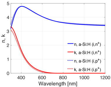
Refractive indices of c-Si, TiO2, ITO, and Ag used in the calculations were taken from literature 26, 27, 28, 29. Refractive index data for the front and rear composite (passivation intrinsic and doped) a-Si:H layers were obtained using ellipsometry, and corresponding and values provided by Meyer Burger Research AG are plotted in Fig. 2. For the window layers, a non-absorbing optically thick glass layer was considered to have a nondispersive refractive index of , and EVA and MgF2 refractive index data was taken from 30 and 31, respectively.
2.2 Simulation framework
The numerical simulations of the EVA-cell interface for both AR and LT TiO2 nanodisk arrays were performed using the finite element method (FEM) with commercial software JCMsuite 32. The annual EY was calculated using a comprehensive modeling framework enabling the quick simulation of various and sophisticated PV architectures under realistic irradiation conditions discussed in detail in 33, 34.
2.3 Electrical parameters
The electrical parameters corresponding to a typical c-Si HJT solar cell used in the annual EY calculation are summarized in Table 1. The shadowing by electrical connections for all considered architectures is disregarded.
| Shunt resistance, [] | 5000 |
|---|---|
| Series resistance, [] | 0.7 |
| Reverse-blocking current, [] | 2 |
| Ideality factor, | 1.1 |
| Temperature coefficient of , [] | 0.05 |
| Temperature coefficient of , [] | -0.25 |
A device characterized by these properties would have a around 38.3 mA/cm2. This yields V at temperature C from the following equation:
| (1) |
where the thermal voltage V, and the values of ideality factor and reverse-blocking current can be found in Table 1.
2.4 Calculation of reflectance, transmittance, and absorptance
At the EVA-cell interfaces with introduced AR and LT nanodisk arrays, reflectance and transmittance into all scattering directions at each wavelength and incidence polar and azimuth angles is calculated as the ratio of the scattered reflected or transmitted power to the power of the incident field. At the considered interfaces, both c-Si and EVA are assumed to be semi-infinite. For a given azimuth angle , reflectance and transimittance values form matrices of the size (, , ), where the entries correspond to all polar angles of incidence, scattering angles, and wavelengths, respectively. The polar angle is varied from to with step, and the results are then interpolated at intervals of . In case of azimuth angle , the symmetry of the nanodisk coating is exploited, and only calculations for angles between and with step are performed. The calculated matrices for different values are subsequently averaged. Total reflectance and transmittance for a certain wavelength and incident polar and azimuth angles are calculated according to:
| (2) |
| (3) |
where are the wave vectors of reflected and transmitted fields, are the scattering angles, is the amplitude of an incident plane wave with a mixed TE-TM polarization, and and are the refractive indices of the media where the incident and scattered waves propagate, respectively. We use the angular spectrum representation of the fields, and in equations 2 and 3 is calculated by means of the Fourier transform of the electric fields in real space obtained from full-wave simulations. Absorptance in each of the thin film layers and nanodisk array was calculated by integrating the divergence of the Poynting vector across the absorber volume, thus yielding absorbed power which is normalized to the power of the incident plane wave. Similarly to reflectance and transmittance, for a given azimuth angle, absorptance values form a matrix of the size (, , ), where index runs over all absorbing layers in the front or rear solar cell stack. The angular dependent simulations were performed for optimized AR and LT nanodisk arrays. The optical performance of the nanodisk arrays was optimized with respect to the short-circuit current associated with reflectance at a normal light incidence, which is calculated using the following equation:
| (4) |
where is the electron charge, is the energy of a photon, and is the spectral irradiance. For this calculation, air mass 1.5 global (AM1.5G) tilted irradiance raw data was taken from 35, and the total reflectance was interpolated accordingly. The short-circuit current due to reflectance was minimized for front nanodisk array and maximized for the rear LT nanodisk array.
Within the EY modeling framework, where the optical response of the entire architecture is computed, the light propagation in multi-layer thin-film stacks is treated coherently, for which the transfer matrix method is employed. When AR and LT nanodisk arrays are considered instead of those thin-film layers, the corresponding output matrices for reflectance, transmittance, and absorptance are integrated into the modeling framework. For thicker layers, such as the c-Si substrate of the cell and window layers of the module, the assumption of coherence breaks down. The Beer-Lambert law can describe the absorption of the light in those layers:
| (5) |
where is the initial intensity, is the absorption coefficient of the considered medium, and is the distance traveled in it.
3 Results and discussion
3.1 Energy yield of solar modules
We analyzed the annual EY of the four solar module architectures introduced in Fig. 1 for three cities in the United States of America located in different climate zones 36. Two of the chosen cities, Anchorage, AK and Honolulu, HI, have highly contrasting irradiation conditions. The former is a cold and cloudy region (Boreal climate) and the latter a hot and sunny one (Tropical climate). The additionally chosen Kansas City, MO, has a temperate climate that receives an annual solar irradiance between Anchorage and Honolulu. By covering different climate zones, we aimed to highlight the robustness of the nanodisk arrays performance and their ability to improve the annual EY for all types of irradiation conditions, albeit with small differences that most likely originate from the spectral features of the nanodisk arrays. The solar modules were considered to face south, and the tilt angles were optimized for each location. This resulted in values to be for Anchorage, for Kansas City, and for Honolulu, respectively.
Figure 3 demonstrates the relative improvement of the annual EY when the nanodisk arrays are used for light management instead of the optimized planar layers. The increase of the annual EY is shown as a function of the c-Si absorber thickness. We considered the case when the AR array is introduced on the front surface of the c-Si HJT cell in the case of the monofacial module architecture, and both AR and LT nanodisk arrays are applied to the front and rear surfaces of the cell in the case of the bifacial module architecture. For this calculation, no albedo was considered. The relative increase of the annual EY reached up to 11.0 % and 43.0 % at the minimal wafer thickness of 5 m for monofacial and bifacial architectures with nanodisks, respectively.
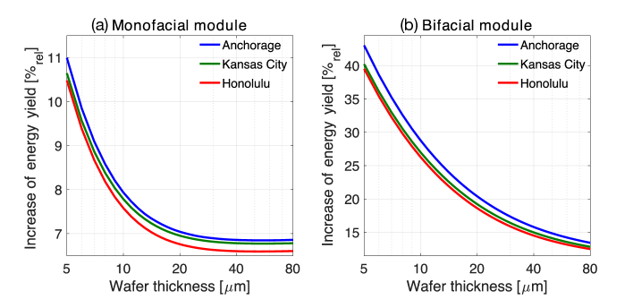
As expected, for the monofacial case, the module with an AR nanodisk array (Fig. 1(b)) outperforms the standard flat architecture with an optimized ITO coating (Fig. 1(a)), with this effect becoming even more apparent when reducing the c-Si absorber thickness. However, the front side AR array with a relatively small size of the individual disks does not have strong LT properties. Its contribution to light harvesting stems mainly from its broadband AR performance. When instead of a full metallic contact, the window encapsulation and glass layers are introduced, to take advantage of the solar irradiation which can hit the module on its back, one has to take care of an appropriate light trapping structure, which would also act as a decent AR coating. For this purpose, an LT nanodisk array was designed (Fig. 1(d)). With the individual disk parameters being significantly larger when compared to the nanodisk array used as the AR structure at the front interface, the light which is not absorbed in the silicon and reaches the rear interface of the cell is effectively scattered in multiple directions, thus improving the LT properties of the cell. From Fig. 3 (b) it can be seen that it translates into an even more significant increase of the annual EY than for monofacial module architecture when comparing to a reference bifacial module architecture (Fig. 1(c)).
If additionally, one considers albedo radiation, the advantage of the bifacial module architecture with AR and LT nanodisk arrays becomes even more apparent. The influence of albedo is shown in Fig. 4. Here, the annual EY of the four module architectures with a selected median c-Si absorber thickness of 40 m is shown for the sandstone and grass ground surface compared to EY of the modules without albedo.
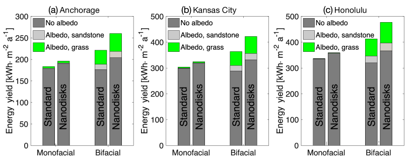
Since the interfaces of the standard reference modules are flat, without albedo, the monofacial standard reference module outperforms the bifacial reference. While for the former, the silver layer reflects the light reaching it back into the cell, for the latter, a lot of light is lost due to transmittance when no LT structure is introduced. This difference is bigger with a smaller module tilt angle since less irradiation can hit the module from the back. However, as soon as albedo radiation is considered, the bifacial standard reference outperforms its monofacial counterpart. While for monofacial architecture albedo radiation does not make a significant difference, one can see a robust improvement in the annual EY for the bifacial case. The increase of the annual EY for the monofacial architecture varies depending on the module tilt and is stronger for locations with a greater (Anchorage). The relative improvement reaches up to around 0.8 % with sandstone and 3.0 % with grass as a ground surface for both the standard reference monofacial module and monofacial module with AR nanodisk array with insignificant difference between them. In the case of the bifacial module architecture, a stronger increase of the annual EY is expected for the sunnier locations (Honolulu). It reaches up to 8.2 % with sandstone, and 28.9 % with grass ground surface in case of a standard reference bifacial module. For a bifacial module with AR and LT structures, the relative increase is 8.3 % and 30.1 % with sandstone and grass ground surface, respectively.
3.2 Optical performance of solar modules
To better understand the mechanism behind the annual EY improvement when the nanodisk arrays are introduced on top of the front and back contacts of a solar cell, one can look at the optical properties of the cell interfaces with the optimized nanodisk arrays. Figure 5 shows reflectance at normal incidence of the EVA-cell interfaces for the front and rear HJT solar cell contacts with AR and LT nanodisk arrays. For both nanodisk arrays and illumination directions, reflectances of the corresponding reference flat interfaces are plotted for comparison. The graphs (a) and (b) in Fig. 5 correspond to the optical response of the front EVA-cell interface. In this case, the objective was to minimize short-circuit current density corresponding to reflectance introduced in Eq. 4, which resulted in an AR nanodisk array with reflectance shown in Fig. 5(a).

This design was based on the previous work on helicity preserving TiO2 nanodisk array for the front interface of a c-Si HJT solar cell, where efficient and broadband backscattering suppression was achieved due to the ability of the system to suppress cross-talk between opposite handednesses of the electromagnetic field upon light-matter interaction 25. The requirement for a system to be helicity preserving is to possess a high enough degree of rotational symmetry () along the illumination direction. For normal light incidence, for which the optimization of AR nanodisk array was performed, the illumination direction is along the symmetry axis of an individual nanodisk, which essentially means that in this case. The resulting reflectance of the AR nanodisk array is lower than the one of the reference optimized flat AR coating and exceeds it slightly only in the wavelength region around nm, for which standard AR coating of the solar cell is typically optimized. However, as shown in Fig. 5(b), the LT properties of this nanodisk array are not as good as its AR properties. When the light is impinging from the c-Si absorber, only the long-wavelength response is relevant since the short-wavelength photons are absorbed before reaching this interface. This nanodisk coating transmits the light reflected from the rear of the stack particularly strongly at longer wavelengths and is not possessing better LT properties than the standard flat reference. This optical response confirms that the front nanodisk array contributes to the light harvesting of the considered solar module architectures mainly by its AR properties.
The graphs (c) and (d) in Fig. 5 demonstrate the optical response of the optimized LT nanodisk array. Here, the structure parameters strongly differ from those of the helicity preserving AR nanodisk array. The larger and more sparsely spaced LT nanodisks allow for improved harvesting of the long-wavelength photons reaching the rear of the solar cell. The impinging light is effectively scattered into multiple directions since many diffraction orders are allowed. Taking into account the absorption depth of c-Si, for the minimal considered absorber thickness of 5 m, the photons that can reach the rear contact of the solar cell have wavelengths nm. The optimized reflectance of the LT nanodisk array for the spectral region of interest is shown in Fig. 5(c). Its LT performance exceeds that of the flat reference solar cell stack at all wavelengths. Nevertheless, as can be seen from Fig. 5(d), though this nanodisk array outperforms its flat reference counterpart in terms of AR properties in the longer wavelength range, overall, its main contribution to the improved absorption in c-Si, and, consequently, the annual EY of the solar module, is due to its superior LT properties. This way, in the bifacial module case, when nanodisk arrays with decoupled AR and LT properties are present on both sides of the solar cell stack, one can achieve a solid overall solar module performance boost.
Another critical aspect of the solar module’s optical performance is parasitic absorption. Here, all discussed results are for a selected median c-Si absorber thickness of 40 m and at normal light incidence. Figures 6 and 7 show absorptance in all layers of the monofacial and bifacial module stacks, respectively, except for the glass layer, which was assumed to be non-absorbing. Additionally, the absorptance of the rear a-Si:H layer in monofacial module configuration and of rear and front a-Si:H layers in the bifacial module configuration for forward and backward illumination direction, respectively, was negligible, and, thus, it is not shown. Moreover, the LT TiO2 nanodisk array, which is considered for the bifacial module configuration, does not introduce any parasitic absorption since the light absorbed in these nanodisks has short wavelengths and does not reach the rear cell interface while it is absorbed in c-Si. The short-circuit current densities indicated on the top of all graphs in Fig. 6 and Fig. 7 were calculated assuming AM1.5G spectrum using the modified Eq. 4 with absorptance of c-Si instead of reflectance.
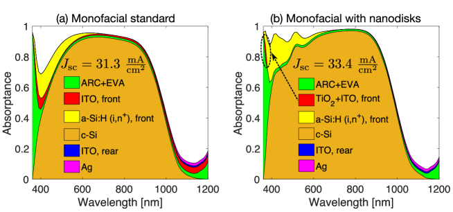
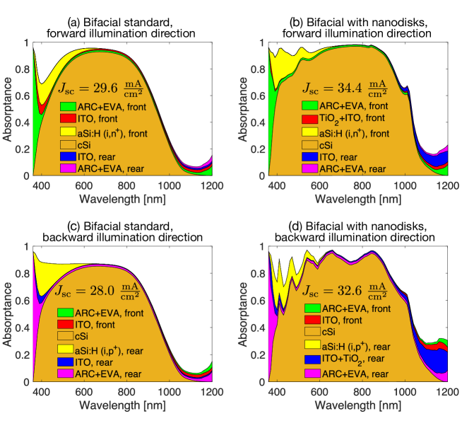
In the case of the monofacial standard reference module (Fig. 6(a)), the front transparent conductive ITO layer serves as an AR coating but also introduces some parasitic absorption. However, when the AR nanodisk array is introduced (Fig. 6(b)), ITO thickness for the optimized front solar cell contact is reduced considerably (from 75 to 10 nm), and parasitic absorption in this layer is significantly reduced. The nanodisks themselves have a tiny contribution to the parasitic absorption, considering that EVA absorbs all the light impinging on the solar module at the wavelengths between 300 and 360 nm and TiO2 absorbs only at wavelengths shorter than nm. On the other hand, while the AR nanodisk array increases the absorptance in c-Si thanks to a better in-coupling of the incident light, it also increases parasitic absorption in the front a-Si:H layer. However, it should be noted that in 37 it was shown that the carriers which are absorbed in an intrinsic a-Si:H layer can still contribute to the short-circuit current, and thus the parasitic absorption loss in this layer represents an upper bound and can have a less of an impact in reality. Thus, introducing the TiO2 AR nanodisk array leads to a broadband enhancement of absorptance in the silicon absorber layer.
In the case of the bifacial standard reference module and forward illumination direction (Fig. 7(a)), the parasitic absorption for the wavelengths below nm is similar to the one of the monofacial module reference. However, the parasitic absorption is slightly lower in the long-wavelength range since more light is transmitted through the glass and encapsulation window layers. When AR and LT nanodisk arrays are introduced (Fig. 7(b)), the front nanodisks improve absorptance in silicon the same way as in the case of the monofacial module. The rear nanodisk array additionally enhances aborptance at longer wavelengths. However, due to the strong scattering enabled by LT nanodisks, parasitic absorption is also increased for longer wavelengths. When the light is impinging on the rear side of the bifacial solar module (Fig. 7(d)), the absorptance in c-Si is also improved in the case when AR and LT arrays are introduced in comparison to the reference flat module (Fig. 7(c)), even though LT nanodisks are not optimal in terms of their AR properties and introduce dips in silicon absorptance due to the sharp spectral features which can be seen in Fig. 5(d).
4 Conclusions
We have numerically studied the annual energy yield (EY) under realistic irradiation conditions for monofacial and bifacial crystalline silicon (c-Si) heterojunction (HJT) solar module architectures with AR and light trapping (LT) titanium dioxide (TiO2) nanodisk square arrays introduced on top of the front and rear ITO layers and compared their power outputs with the ones of the corresponding standard reference flat solar modules. We have shown that while reducing the silicon absorber thickness, the relative increase of the annual EY is reaching up to 11.0 % and 43.0 % for monofacial and bifacial modules with nanodisk coatings, respectively. This improvement is comparable for the locations with different climate conditions. Moreover, in the case of bifacial module architecture, taking into account the albedo radiation produces an additional boost of the module performance.
The designed dielectric nanodisk arrays for the front and rear contacts of c-Si HJT solar cell have both a significant impact on the light absorption in the c-Si wafer. At the same time, their AR and LT properties are decoupled. The front AR nanodisk array has a relatively small individual disk size and lattice constant, and its broadband backscattering suppression is related to the helicity preservation condition. In contrast, the rear LT nanodisk array has larger features and array pitch and allows for efficient scattering into multiple scattering directions. Furthermore, these AR and LT nanodisk square array designs are not restricted to a specific material or a particular photovoltaic solar cell stack and, thus, can be investigated for different solar module configurations.
The authors acknowledge support by the state of Baden-Württemberg through bwHPC and the German Research Foundation (DFG) through grant no INST 40/575-1 FUGG (JUSTUS 2 cluster). The authors are also grateful to JCMwave for their free provision of the FEM Maxwell solver JCMsuite.
References
- Shockley and Queisser 1961 Shockley, W.; Queisser, H. J. Detailed Balance Limit of Efficiency of p‐n Junction Solar Cells. Journal of Applied Physics 1961, 32, 510–519
- Richter et al. 2017 Richter, A.; Benick, J.; Feldmann, F.; Fell, A.; Hermle, M.; Glunz, S. W. n-Type Si solar cells with passivating electron contact: Identifying sources for efficiency limitations by wafer thickness and resistivity variation. Solar Energy Materials and Solar Cells 2017, 173, 96–105
- Seidel et al. 1990 Seidel, H.; Csepregi, L.; Heuberger, A.; Baumgärtel, H. Anisotropic Etching of Crystalline Silicon in Alkaline Solutions: I . Orientation Dependence and Behavior of Passivation Layers. Journal of The Electrochemical Society 1990, 137, 3612–3626
- Liu et al. 2020 Liu, Z.; Sofia, S. E.; Laine, H. S.; Woodhouse, M.; Wieghold, S.; Peters, I. M.; Buonassisi, T. Revisiting thin silicon for photovoltaics: a technoeconomic perspective. Energy & Environmental Science 2020, 13, 12–23
- Haegel et al. 2019 Haegel, N. M. et al. Terawatt-scale photovoltaics: Transform global energy. Science 2019, 364, 836–838
- Garnett et al. 2021 Garnett, E. C.; Ehrler, B.; Polman, A.; Alarcon-Llado, E. Photonics for Photovoltaics: Advances and Opportunities. ACS Photonics 2021, 8, 61–70
- Green and Pillai 2012 Green, M. A.; Pillai, S. Harnessing plasmonics for solar cells. Nature Photonics 2012, 6, 130–132
- Catchpole and Polman 2008 Catchpole, K.; Polman, A. Plasmonic solar cells. Opt. Express 2008, 16, 21793–21800
- Ferry et al. 2008 Ferry, V. E.; Sweatlock, L. A.; Pacifici, D.; Atwater, H. A. Plasmonic Nanostructure Design for Efficient Light Coupling into Solar Cells. Nano Letters 2008, 8, 4391–4397
- Hou et al. 2020 Hou, J.; Yang, B.; Li, X.; Ma, C.; Wang, B.; Long, H.; Yang, C.; Chen, S. Efficient and stable thin-film crystalline silicon solar cell by introducing rotation factor in surface square pillar array grating. Journal of Nanophotonics 2020, 14, 016008
- He et al. 2016 He, J.; Yang, Z.; Liu, P.; Wu, S.; Gao, P.; Wang, M.; Zhou, S.; Li, X.; Cao, H.; Ye, J. Enhanced Electro-Optical Properties of Nanocone/Nanopillar Dual-Structured Arrays for Ultrathin Silicon/Organic Hybrid Solar Cell Applications. Advanced Energy Materials 2016, 6, 1501793
- Spinelli et al. 2015 Spinelli, P.; Lenzmann, F.; Weeber, A.; Polman, A. Effect of EVA Encapsulation on Antireflection Properties of Mie Nanoscatterers for c-Si Solar Cells. IEEE Journal of Photovoltaics 2015, 5, 559–564
- Yalamanchili et al. 2020 Yalamanchili, S.; Verlage, E.; Cheng, W.-H.; Fountaine, K. T.; Jahelka, P. R.; Kempler, P. A.; Saive, R.; Lewis, N. S.; Atwater, H. A. High Broadband Light Transmission for Solar Fuels Production Using Dielectric Optical Waveguides in TiO2 Nanocone Arrays. Nano Lett. 2020, 20, 502–508
- Spinelli et al. 2012 Spinelli, P.; Verschuuren, M.; Polman, A. Broadband omnidirectional antireflection coating based on subwavelength surface Mie resonators. Nature Communications 2012, 3, 1–5
- Hou et al. 2017 Hou, J.; Hong, W.; Li, X.; Yang, C.; Chen, S. Biomimetic spiral grating for stable and highly efficient absorption in crystalline silicon thin-film solar cells. Optics Express 2017, 25, A922–A931
- Wang et al. 2012 Wang, K. X.; Yu, Z.; Liu, V.; Cui, Y.; Fan, S. Absorption Enhancement in Ultrathin Crystalline Silicon Solar Cells with Antireflection and Light-Trapping Nanocone Gratings. Nano Letters 2012, 12, 1616–1619
- Isabella et al. 2018 Isabella, O.; Vismara, R.; Linssen, D.; Wang, K.; Fan, S.; Zeman, M. Advanced light trapping scheme in decoupled front and rear textured thin-film silicon solar cells. Solar Energy 2018, 162, 344–356
- Singh et al. 2021 Singh, M.; Santbergen, R.; Syifai, I.; Weeber, A.; Zeman, M.; Isabella, O. Comparing optical performance of a wide range of perovskite/silicon tandem architectures under real-world conditions. Nanophotonics 2021, 20200643
- Hörantner and Snaith 2017 Hörantner, M. T.; Snaith, H. J. Predicting and optimising the energy yield of perovskite-on-silicon tandem solar cells under real world conditions. Energy Environ. Sci. 2017, 10, 1983–1993
- Tucher et al. 2019 Tucher, N.; Höhn, O.; Murthy, J. N.; Martinez, J. C.; Steiner, M.; Armbruster, A.; Lorenz, E.; Bläsi, B.; Goldschmidt, J. C. Energy yield analysis of textured perovskite silicon tandem solar cells and modules. Optics Express 2019, 27, A1419–A1430
- Lehr et al. 2020 Lehr, J.; Langenhorst, M.; Schmager, R.; Gota, F.; Kirner, S.; Lemmer, U.; Richards, B. S.; Case, C.; Paetzold, U. W. Energy yield of bifacial textured perovskite/silicon tandem photovoltaic modules. Solar Energy Materials and Solar Cells 2020, 208, 110367
- Gota et al. 2020 Gota, F.; Langenhorst, M.; Schmager, R.; Lehr, J.; Paetzold, U. W. Energy Yield Advantages of Three-Terminal Perovskite-Silicon Tandem Photovoltaics. Joule 2020, 4, 2387–2403
- Jošt et al. 2018 Jošt, M.; Köhnen, E.; Morales-Vilches, A. B.; Lipovšek, B.; Jäger, K.; Macco, B.; Al-Ashouri, A.; Krč, J.; Korte, L.; Rech, B., et al. Textured interfaces in monolithic perovskite/silicon tandem solar cells: advanced light management for improved efficiency and energy yield. Energy & Environmental Science 2018, 11, 3511–3523
- Russell et al. 2017 Russell, T. C. R.; Saive, R.; Augusto, A.; Bowden, S. G.; Atwater, H. A. The Influence of Spectral Albedo on Bifacial Solar Cells: A Theoretical and Experimental Study. IEEE Journal of Photovoltaics 2017, 7, 1611–1618
- Slivina et al. 2019 Slivina, E.; Abass, A.; Bätzner, D.; Strahm, B.; Rockstuhl, C.; Fernandez-Corbaton, I. Insights into Backscattering Suppression in Solar Cells from the Helicity-Preservation Point of View. Physical Review Applied 2019, 12, 054003
- Schinke et al. 2015 Schinke, C.; Christian Peest, P.; Schmidt, J.; Brendel, R.; Bothe, K.; Vogt, M. R.; Kröger, I.; Winter, S.; Schirmacher, A.; Lim, S.; Nguyen, H. T.; MacDonald, D. Uncertainty analysis for the coefficient of band-to-band absorption of crystalline silicon. AIP Advances 2015, 5, 067168
- 27 Filmetrics database, TiO2 Rutile. \urlhttps://www.filmetrics.com/refractive-index-database
- Holman et al. 2013 Holman, Z. C.; Filipič, M.; Descoeudres, A.; De Wolf, S.; Smole, F.; Topič, M.; Ballif, C. Infrared light management in high-efficiency silicon heterojunction and rear-passivated solar cells. Journal of Applied Physics 2013, 113, 013107
- Jiang et al. 2016 Jiang, Y.; Pillai, S.; Green, M. A. Realistic Silver Optical Constants for Plasmonics. Scientific Reports 2016, 6, 1–7
- McIntosh et al. 2009 McIntosh, K. R.; Cotsell, J. N.; Cumpston, J. S.; Norris, A. W.; Powell, N. E.; Ketola, B. M. An optical comparison of silicone and EVA encapsulants for conventional silicon PV modules: A ray-tracing study. 2009 34th IEEE Photovoltaic Specialists Conference (PVSC). Philadelphia, PA, USA, 2009; pp 000544–000549
- Siqueiros et al. 1988 Siqueiros, J. M.; Machorro, R.; Regalado, L. E. Determination of the optical constants of MgF2 and ZnS from spectrophotometric measurements and the classical oscillator method. Applied Optics 1988, 27, 2549–2553
- Pomplun et al. 2007 Pomplun, J.; Burger, S.; Zschiedrich, L.; Schmidt, F. Adaptive finite element method for simulation of optical nano structures. Physica Status Solidi B 2007, 244, 3419–3434
- Schmager et al. 2019 Schmager, R.; Langenhorst, M.; Lehr, J.; Lemmer, U.; Richards, B. S.; Paetzold, U. W. Methodology of energy yield modelling of perovskite-based multi-junction photovoltaics. Optics Express 2019, 27, A507–A523
- 34 EYcalc - Energy yield calculator for multi-junction solar modules with realistic irradiance data and textured interfaces. \urlhttps://github.com/PerovskitePV/EYcalc
- Gueymard et al. 1995 Gueymard, C., et al. SMARTS2: a simple model of the atmospheric radiative transfer of sunshine: algorithms and performance assessment; Florida Solar Energy Center Cocoa, FL, 1995
- Peel et al. 2007 Peel, M. C.; Finlayson, B. L.; McMahon, T. A. Updated world map of the Köppen-Geiger climate classification. Hydrology and earth system sciences 2007, 11, 1633–1644
- Holman et al. 2012 Holman, Z. C.; Descoeudres, A.; Barraud, L.; Fernandez, F. Z.; Seif, J. P.; De Wolf, S.; Ballif, C. Current Losses at the Front of Silicon Heterojunction Solar Cells. IEEE Journal of Photovoltaics 2012, 2, 7–15