Coherent-scatterer enhancement and Klein-tunneling suppression by potential barriers in gapped graphene with chirality-time-reversal symmetry
Abstract
We have utilized the finite-difference method to investigate electron tunneling in gapped graphene across various electrostatic-potential barriers. Specifically, we analyze Gaussian and triangular envelope functions to compare with a square potential barrier. The transmission coefficient was calculated numerically for each case and applied to corresponding tunneling conductance. It is well known that Klein tunneling in graphene will be greatly reduced in a gapped graphene. Our results further demonstrated that such a decrease of transmission can be significantly enhanced for spatially-modulated potential barriers. Additionally, we investigated the effect from a bias field applied to those barrier profiles, from which we showed that it enables the control of electron flow under normal incidence. The suppression of Klein tunneling was found to be more severe for a non-square barrier and exhibits a strong dependence on bias-field polarity for all kinds of barriers. The roles played by a dilute distribution of point impurities on electron transmission and conductance were analyzed with a sharp peak appearing in the electron conductance as an impurity atom is placed in the middle of a square barrier. However, for narrow triangular and Gaussian barriers, the conductance peaks become substantially broadened, associated with an enhancement of the tunneling conductance.
I Introduction
The unusual properties of Dirac quasiparticles have become one of the most popular topics in fundamental research as well as a promising source for new technological applications Geim and Novoselov (2010); Neto et al. (2009); Geim (2009). Being a zero-bandgap semiconductor and possessing a specific chiral wave function simultaneously will result in full transparency for any potential barrier for normally-incident electrons. Beenakker (2008); Katsnelson et al. (2006) A massless Dirac fermion which is scattered by an electrostatic potential is able to tunnel with certainty for normal incidence, as known Klein paradox, regardless of the potential-barrier height or width. Klein (1929); Calogeracos and Dombey (1999) Graphene is also known for its specific magnetic-field properties, Goerbig (2011); Gumbs et al. (2014a); Pyatkovskiy and Gusynin (2011); Checkelsky and Ong (2009) as well as its strong decrease of magneto-resistance Huang et al. (2019); Kim and Kim (2008) through - junctions. Cheianov and Fal’ko (2006) While the metallic band structure and high mobility are obvious advantages of graphene, most applications in electronics require a small and tunable bandgap Pereira et al. (2008) in order to keep its charged carriers confined within a finite area of an electronic device. Berger et al. (2006) This feature could be achieved by opening a finite bandgap Ni et al. (2008) which directly leads to a suppression of the Klein tunneling in graphene. Iurov et al. (2011); Kindermann et al. (2012); Zhou et al. (2007); Iurov et al. (2013)
There are various efficient ways for creating a sizable (meV and above) and tunable bandgap in graphene. Most of them are generated byadding a dielectric Si-based substrate Ni et al. (2008) or a substrate with broken inversion symmetry between sublattices. Zhou et al. (2007) It was just recently discovered that a tunable gap can be achieved after a Dirac-cone hexagonal two-dimensional (2D) lattice has been irradiated with a circularly-polarized Iurov et al. (2019); Oka and Aoki (2009); Liu et al. (2011) and off-resonance field Iurov et al. (2020a); Pastrana-Martinez et al. (2012); Usaj et al. (2014); Iurov et al. (2017a); Kibis (2010); Pervishko et al. (2015); Portnoi et al. (2008); Kibis et al. (2017); Iurov et al. (2017b); Dey and Ghosh (2018). In addition, strain engineering, finite-width graphene nanoribbon (GNR) systems, Brey and Fertig (2006), structural and topological defects or insertion of impurity atoms can also produce a bandgap in graphene. Pereira et al. (2008) Physically, the presence and size of an induced bandgap in graphene and other hexagon lattices directly affect tunneling and transport properties Kristinsson et al. (2016); Iurov et al. (2020b), and play a crucial role in graphene-based electronics, such as field-effect transistors since their on/off current ratios Low and Appenzeller (2009) can be tuned through tunneling control. Also, the optical response of gapped graphene acquire attractive features in opto-electronics and optical spectroscopy. Pedersen et al. (2009) Particularly, these responses have been proved to be sensitive to localized and trapped states within the bandgap of systems considered. Pereira et al. (2006); Gumbs et al. (2014b); Castro et al. (2008) The effect due to mesoscopic fluctuations appearing in the conductance of a gapped-graphene strip arising from a random electrostatic potential landscape is believed to be important but has not been investigated thoroughly as for gapless graphene. Rycerz et al. (2007) The same goes for the effect of an electrostatic field applied across a potential barrier. Jang et al. (2013)
Although a considerable amount of research has been published on graphene band-transport characteristics, investigations on tunneling across a smoothly-varying potential barrier in a gapped Dirac system have been much less dealt with. In fact, tunneling transport through a steep-slope potential profile, involving either single or double square barrier, has been investigated and reported in Refs. [Dahal and Gumbs, 2017; Azarova and Maksimova, 2014; Navarro-Giraldo and Quimbay, 2018]. However, analytical solutions for a finite-slope barrier are still inaccessible. On the other hand, electron transmission in graphene and other newly discovered Dirac materials was also computed based on Wentzel-Kramers-Brillouin (WKB) semiclassical theory. Sonin (2009); Weekes et al. (2021) Furthermore, it has been shown within WKB theoru that if electron-hole transition is considered inside a non-square potential barrier, tunneling transmission will increase with the slope of a potential profile. Technically, a smooth finite-slope potential barrier becomes more realistic since it matches better with the experimentally accessible situation Stander et al. (2009). Importantly, such a case also presents several intriguing phenomena and properties, e.g., Klein collimator Libisch et al. (2017) as well as a possibility for building up a collimated interferometer or reflector Young and Kim (2009); Wang et al. (2019). Besides, these smooth-barrier profiles also display unusual tunneling features upon applying an electric or a magnetic field. Mouhafid and Jellal (2013); Shytov et al. (2008); Young and Kim (2009); Anwar et al. (2017); Anwar (2020)
Compared with tunneling transport of incident electrons through a potential barrier in graphene, impurity scattering Titov (2007); Ando and Koshino (1984); Rycerz et al. (2007); Anwar et al. (2020) in gapped graphene turns out to be another important research topic that has not been adequately studied. Disorder embedded within an electrostatic-potential barrier in a gapped graphene system Huang et al. (1999), which exhibits either disorder-assisted or disorder-impeded tunneling, is even less known. Specifically, the spatial position, strength and polarity of an embedded scatterer and its effect on tunneling conductance of electrons for various electrostatic potential barriers Rycerz et al. (2007); Titov (2007) have become the most important aspect because they decide whether the conductance of the system is enhanced or reduced by different impurity configurations. As a result, it is of paramount importance to study the effect of impurity scattering in gapped graphene and reveal the condition for suppressed back-scattering of incident electrons by appropriately distributing scatterers within a barrier region, and this makes a crucial part of our current work.
The key issue addressed in this paper is quantifying electron transmission and conductance across non-square potential barriers with a finite slope in gapped graphene subject to a DC electric field by using a discretized Dirac equation Hernández and Lewenkopf (2012); Tworzydło et al. (2008) based on a finite-difference method Anwar et al. (2020); Huang et al. (2020). Our numerical method presented here has proven to be crucial for studying a gapped-graphene system with a smooth disorder potential. Based on our established numerical procedure, we hsvr accurately calculate the effect of a disorder potential on electron tunneling and conductance. The remainder of the paper is organized as follows. We first validate our discretized model by calculating the transmission coefficient of gapped graphene across a potential barrier, and then compare the obtained numerical results with previous analytical solutions Setare and Jahani (2010) in some limiting cases. By employing this numerical method, we further explore quantitatively how the barrier-potential profile, applied bias with different polarities and barrier-embedded disorders affect the conductance as a function of incident-electron kinetic energy for various graphene - junction (GPNJ) within a gapped monolayer graphene.
II General Formalism
The low-energy states of gapped graphene can be described fully by a Dirac Hamiltonian with an additional gap term, Setare and Jahani (2010); Iurov et al. (2011); Pyatkovskiy (2008) given by
| (1) |
where are three two-dimensional Pauli matrices, is a unit matrix, is the Fermi velocity, is the gap parameter, and represents a spatially non-uniform barrier potential. For constant potential , the Dirac Hamiltonian in Eq. (1) gives rise to a finite energy bandgap between the valence and conduction bands which are symmetric with respect to the Dirac point. In addition, the energy dispersions are calculated as and is a two-dimensional wave vector of electrons. For varied , however, we have , corresponding to electron and hole states, respectively, where is a sign function. This implies that the carrier could go through an electron-hole (or inverse) transition inside the barrier region.
In this paper, we look forward to finding scattering-state solutions for the Hamiltonian in Eq. (1) in the form two-component (spinor) type of wave function, i.e.
| (2) |
where unlike gapless graphene both components rely on the electron-hole index .
As a special case, if is a constant, the translational symmetry of the system is preserved in both and directions, and then the Hamiltonian in Eq. (1) can be greatly simplified as
| (3) |
where , , within the barrier region, and is the given energy of an incident electron. In this case, the scattering-state wave function associated with the Hamiltonian in Eq. (3) takes the explicit form Pyatkovskiy (2008); Iurov et al. (2011, 2017c)
| (4) |
where , for an electron with and for a hole with . Here, two components of the wave function spinor in Eq. (4) are not the same and their ratio further depends on the electron/hole index .
Here, we concentrate on studying the electron transmission and conductance through a biased barrier of different geometries in gapped graphene. Therefore, we limit our investigation only to experimentally-available symmetrical barrier profiles, e.g., triangular and Gaussian shapes. For this reason, we would like to compare our results first with the well-studied case having a square barrier
| (5) |
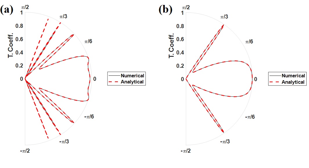
where is the Heaviside step function, meaning if and is equal to zero otherwise. As adopted in Figs. 1 and 2, the selection of using a square potential barrier makes it simple to compare our numerical results for a general varying-slope barrier system with some known analytical cases and discern quantitatively the effect of a finite slope of a potential barrier.
Next, for comparison we would introduce a triangular barrier with both positive and negative slopes present on its two sides, yielding
| (6) |
For our numerical computations, we adopt a symmetric triangular barrier configuration which corresponds to , as used in Fig. 3.
For comparison with experimentally-available setup, we also consider a (symmetric) Gaussian profile with the potential voltage profile varying according to
| (7) |
where is employed to define the effective width of our barrier, is its symmetric center where the highest possible potential is reached, as employed in Fig. 3. Depending on the sign in Eq. (7), this profile could describe either a barrier () or a trap ().
For numerical computations, using the Hamiltonian in Eq. (1) we obtain a pair of coupled scattering-state equations within the barrier region, leading to
| (8) | |||
| (9) |
In Eqs. (8) and (9), when we consider a tilted barrier under an applied electric field , we should replace by within the barrier region, where can be either positive or negative. Additionally, remains conserved during a tunneling process for all regions considered, i.e., on the left of the barrier , , inside , , and to right of the barrier , . We also introduce in Eqs. (8) and (9) a single scatterer of strength at the position within the barrier region for . The scattering problem is such that there could be both transmitted and reflected waves with the amplitudes and , , in regions and but only the transmitted wave in region .
From a physical point of view, it is very instructive to note that under the replacements and for as well, Eq. (9) transforms to Eq. (8) and vice versa. This implies a hidden chirality-time-reversal (CTR) symmetry for electron tunneling in this gapped-graphene system if its scatterer-embedded potential remains unchanged under the barrier transformation with respect to for fixed barrier width , i.e., should acquire a mirror symmetry with respect to its midpoint under zero bias condition.
III Results and Discussions
In order to ensure that our numerically calculated results based on the finite-difference approach (FDA) are accurate and valid, we first compare them with some previously known cases having analytical solutions Setare and Jahani (2010) for a square barrier with . As a validation, we have presented in Fig. 1 the transmission coefficient for a square barrier using both our FDA results and the known analytical solutions Setare and Jahani (2010). This direct comparison clearly indicates that the FDA will be valid for an arbitrary biased barrier potential profile on the order of -meV, including both Gaussian and triangular potential barriers embedded with a single scatterer.
The analytically-calculated transmission coefficients for a 1D square-barrier potential are plotted in Fig. 2 as functions of bandgap parameter for various barrier widths and incoming particle energies . We see clearly from Fig. 2 that the transmission coefficient for head-on collision will be completely suppressed once exceeds an -dependent threshold value, which becomes largely independent of the barrier width . However, this threshold value for reduces with increasing incident-electron energy .
We now turn our attention to numerical computations of the transmission probability by introducing general FDA method, as described in Eqs. (8) and (9), for arbitrary shape of barrier potential profiles under an applied bias field and with embedded point scatterers.
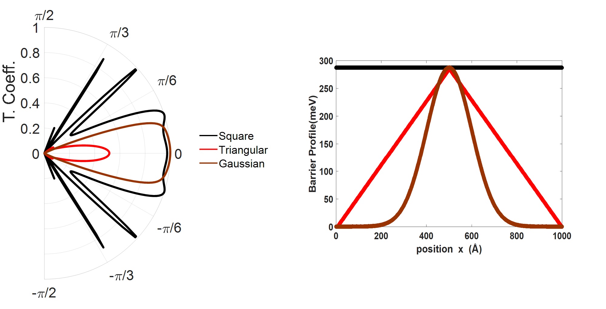
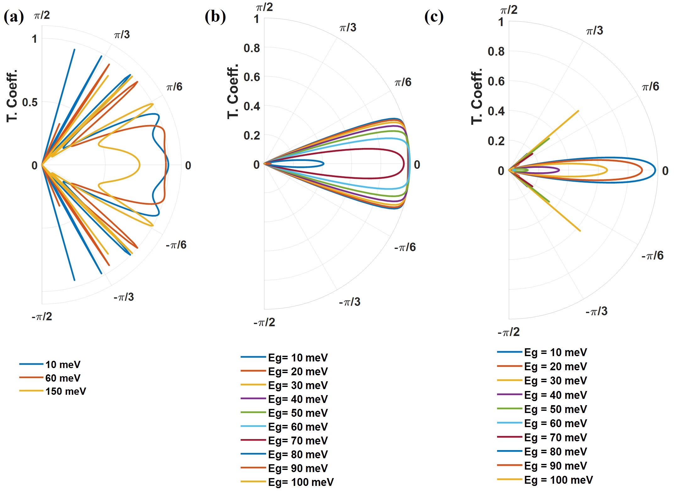
We first present results for the effect of a barrier potential profile on the transmission probability in the absence of a bias field . We have specifically selected square, triangular and Gaussian as three distinctive barrier profiles in Fig. 3 in order to acquire a full comparison among them. From the left panel of Fig. 3, we find a great suppression of Klein tunneling in the presence of a finite gap by a triangular-barrier potential (red curve). Meanwhile, the transmission for this case is only limited to a very narrow angular region around . For a square barrier potential (black curve), on the contrary, the transmission is distributed widely within a broad angular region bounded by , and meanwhile the transmission for head-on collision at remains strong. The transmission for a Gaussian potential barrier (brown curve) somewhat stands between the previous two cases with a limited angular distribution as well as a greatly enhanced strength at compared to a square-barrier and triangular barrier potentials, respectively.
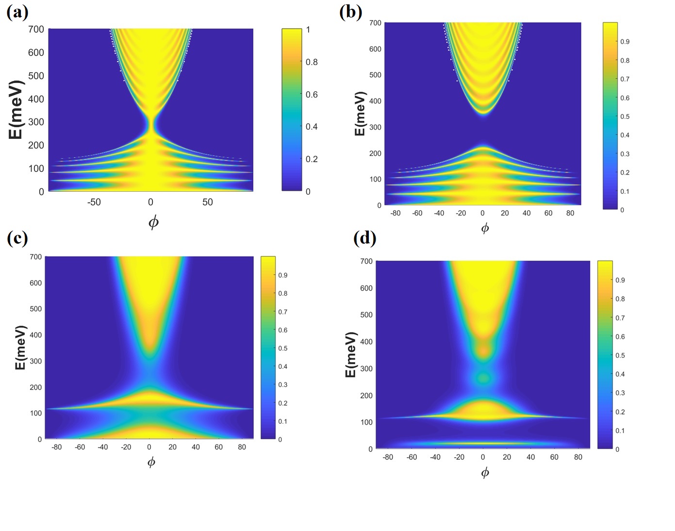
In order to obtain a better and convincing understanding of the effect due to chosen potential barrier-profiles on the transmission probability, we present in Fig. 4 the density plot for as functions of incident-electron energy and incident angle for various barrier profiles. Comparing Figs. 4 and 4, we identify a dominant feature in this figure for the tunneling of electrons in gapped graphene, i.e., the transmission probability can be substantially reduced and nearly goes to zero as the incident energy approaches the barrier height at normal incidence, where the incident particle acquires a small or even imaginary momentum within the barrier region. Additionally, the electron transmission is modified significantly for two different slowly-varying barrier profiles considered in Figs. 4 and 4. Here, many layered sharp resonant features of the transmission probability observed in Fig. 4 for an under square-barrier incidence disappear in both Figs. 4 and 4, leaving only a single energy range around in Fig. 4.
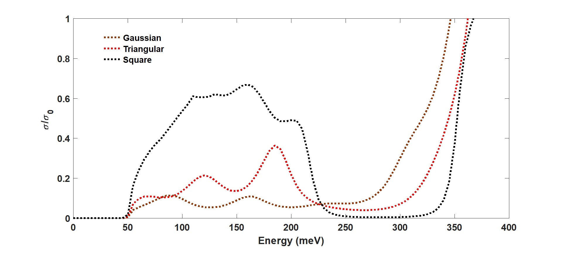
From a technology perspective, we know that the control of an electrical current flow in graphene devices becomes crucial for their applications, such as current modulation, amplification and signal processing. For this reason, we compare in Fig. 5 the changes of scaled tunneling conductance as functions of incoming-particle energy in gapped graphene for three distinct barrier profiles. As shown in Fig. 5, for within the range of -meV, a square barrier gives rise to a square-like highest conductivity (black curve) which, however, is decreased as approaches meV. For a triangular barrier (red curve). On the other hand, we find a strongly-oscillating conductance with multiple peaks and valleys in the same range. Quite differently, Gaussian barrier (brown curve) leads to the lowest weakly-oscillating conductivity for all barrier profiles considered within this energy range, but it produces the highest step-rising conductivity above this energy range. Meanwhile, unlike the square barrier, the conductivity associated with either triangular or Gaussian potential barrier rises quickly for meV although its increase is not as rapid as that for the square potential barrier around meV.
In Fig. 6, for three chosen barrier-potential profiles, we compare the obtained numerical results for the transmission probability as a function of the angle of incidence with a series of gap parameters . For the Gaussian barrier profile in Fig. 6, the tunneling is confined well within a small angle region. With increasing , the tunneling amplitude at is enhanced quickly to unity which is accompanied by the expanded angle region around . Interestingly, very strong focusing of tunneling with respect to is developed for a triangular barrier profile in Fig. 6 which is supplemented by the appearance of two symmetrical sharp side features. Additionally, in this case the tunneling amplitude at is rapidly reduced with increasing , which further goes together with the suppression of the two side features. For the square barrier profile in Fig. 6, lots of side peaks occur and their angle distributions are shrunken slowly as is increased.
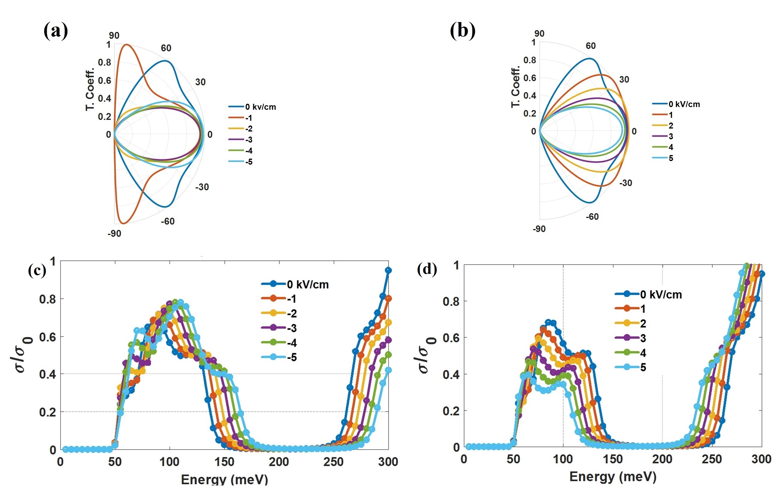
From a device point of view, tuning the tunneling conductance in gapped graphene is an effective technique and very important for its functionality and application. Here, we demonstrate tunable tunneling conductance for gapped graphene by applying a bias field to a general barrier potential , which is in interplay with the opened bandgap of graphene. We start with a square barrier and present calculated polar plots of in Fig. 7- for forward and both backward biases from which we find the suppression of Klein tunneling at due to electron-hole transition resulting from a finite chosen but it is still robust against the applied bias field . It is interesting to note that the suppression of transmission under normal incidence appears only for a positive biase but not for a negative bias, which exhibits a strong asymmetry with respect to the polarity of or broken CTR symmetry in the system. In particular, enhancements of near are seen only for kV/cm. On the other hand, there exists an insulating zero-conductance gap for incident electron energy which follows from Fig. 7-, but its two edges shift in opposite directions with the polarity of . In this way, we can easily switch the electron tunneling conductance between the conducting and insulating phases in gapped graphene by properly selecting the polarity and magnitude of an applied bias field for any fixed kinetic energy of incident electrons.
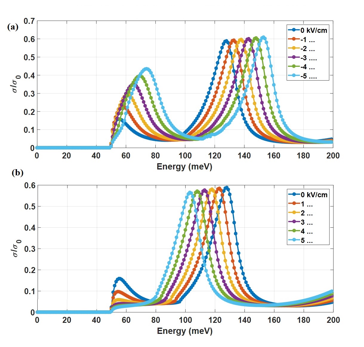
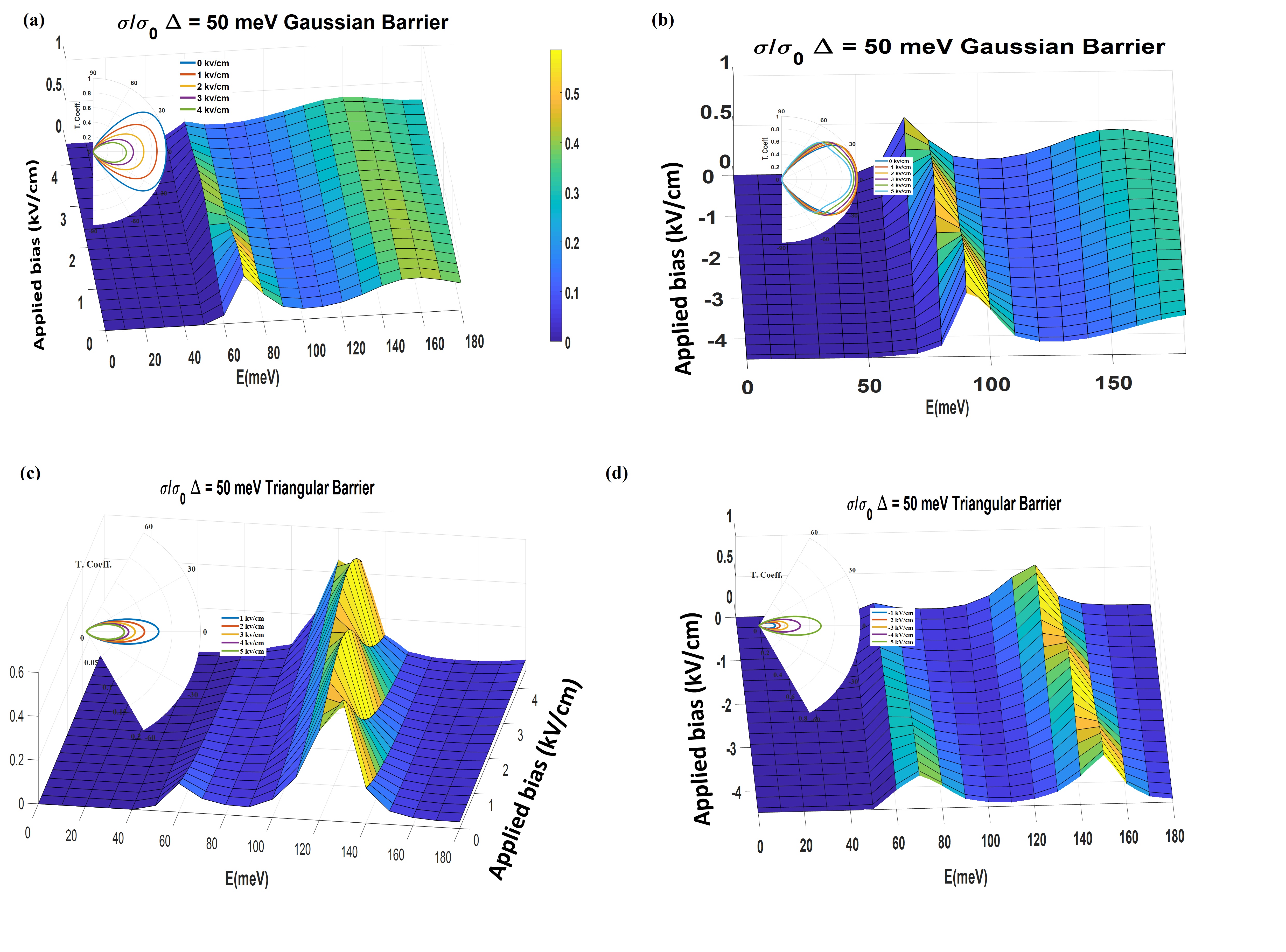
We have established that for a finite bandgap of graphene, the tuning of tunneling conductance by an applied bias field also depends on the selected shape of a barrier potential profile, such as a triangular or Gaussian barrier. For the triangular barrier under a reverse bias in Fig. 8, we find the conductance as a function of remains at zero for meV. However, both the dominant higher and the secondary lower conductance peaks move upward as a function of incoming electron energy with increasing . On the contrary, these two conductance peaks are shifted to smaller values of with increased under forward biases, as found from Fig. 8. In order to gain an overall picture regarding the tuning of tunneling conductance by a bias field for different barrier profiles , we compare corresponding density plots of scaled as functions of both incoming-particle energy and in Figs. 9-9. Generally speaking, the case for biased Gaussian barriers in Figs. 9-9 only gives rise to two relatively-weak peaks in tunneling conductance within two separate ranges for kinetic energy . The bias field , on the other hand, only shifts those conductance peaks in downward in under the forward-bias condition but shifts it upward as a function of in the reverse-bias condition. For a triangular barrier, we find enhanced features for peak shifting both upward and downward with increasing , as displayed in Figs. 9-9.
In the remaining part of this Section, we will address the effect of a single scatterer embedded at various positions within an unbiased barrier of different shapes on tunneling conductance of electrons in gapped graphene. In Fig. 10, we plot for an unbiased square barrier with different locations for a single scatterer. As a comparison, we also display the result with no scatterer in Fig. 10 under for a square barrier potential. From Fig. 10 with , we observe that acquires several consecutive peaks and valleys within the low-energy range of in the presence of a single scatterer. In addition, a zero-conductance gap exists for the intermediate energy range , and meanwhile, a number of peaks and valleys develop for enhanced in the high-energy region . As in Fig. 10 for the scatterer located right in the middle of thr square barrier, a sharp peak in occurs at within this zero-conductance gap, despite the sign and magnitude of . For in Fig. 10, we verify CTR symmetry with respect to the center of a one-dimensional (1D) barrier, i.e., for a scatterer at is the same as for a scatterer at .
In order for us to understand quantitatively the interplay between effects due to a scatterer and the shape of a barrier potential, we compare 2D plots in Figs. 11 and 12 for the scaled tunneling conductance of gapped graphene in the presence of a single scatterer at different positions within a triangular and Gaussian barrier regions. First, for a triangular barrier in Fig. 11, we observe a conductance peak at for instead of as in Fig. 10. Moreover, remains zero within the energy ranges of as well as . As the scatterer is shifted to , we find a weak conductance peak appearing near in Fig. 11. Furthermore, when , we reveal a new strong conductance peak for in Fig. 11 due to constructive superposition of two individual peaks. In particular, the CTR symmetry with respect to the center of a 1D barrier in Fig. 10 is still maintained in Figs. 11 and 11 in comparison with Figs. 11 and 11, respectively, with a switched sign for .
Finally, for a Gaussian potential barrier, we learn from Fig. 12 that there exist two weak conductance peaks at and for in Fig. 12. Additionally, zero-conductance gap is still present within the energy ranges of and . Interestingly, there is a suppression of for incident energy below the barrier height as , as shown in Fig. 12. After increases to at the peak position of a Gaussian barrier in Fig. 12, the shape of as a function of changes drastically by displaying a high and wide constructive conductance peak at accompanied by an overall enhancement of conductance in the energy range of . Furthermore, the CTR symmetry associated with for a 1D barrier is retained in Figs. 12 and 12 compared to Figs. 12 and 12 with a switched sign for .
IV Summary and Concluding Remarks
In a summary, we have thoroughly investigated tunneling and calculated the crucial transmission properties of electrons across square, triangular and Gaussian potential barriers embedded with a single scatterer for gapped graphene. For this, we employed a finite difference approach since their computations are not accessible by standard analytical solution techniques. We have also addressed the effect of a bias and point scatterer located within the barrier. It is known that the transmission and conduction in gapped graphene are largely suppressed as the particle energy lies inside the bandgap inside a barrier region. Due to the existence of a finite bandgap between valence and conduction bands, the Klein tunneling for head-on collision (i.e., with incident angle ) is suppressed for the case with a square potential barrier. Simultaneously, the side resonances for electron tunneling, which are associated with finite incident angles, are also reduced significantly in gapped graphene. These suppression effects become even more pronounced for smooth barriers. However, we have demonstrated multiple ways to modify or even break this low-conduction condition and substantially improve the collimation of transmitted electron beam by employing the approach described above. Using the obtained transmission probability, we have further calculated the tunneling conductance which also displays a suppression for a finite gap in graphene. In fact, we have found that both the transmission and conductance display a strong dependence on the barrier profile, its slope and curvature. Meanwhile, we have also shown that the application of a bias field and its polarity greatly affect the Klein tunneling suppression resulting from broken CTR symmetry of the system, and at the same time shift conductance peaks in energy for all barrier types.
Under a bias field, a zero-conductance gap occurs for a square barrier in a range of selected incident-electron energy below the top of the barrier. For positive/negative bias, two edges of this zero-conductance gap are respectively dragged to lower/higher energies for incident electrons with increasing absolute value of the bias. For a triangular barrier, on the other hand, we have found only one dominant and another secondary peaks in higher and lower energy ranges for incident electrons. Similar behaviors of peak shifting have been seen with increasing . By introducing a single scatterer to an energy barrier of gapped graphene, we have revealed that its strength, polarity and position can affect the conductance profile of gapped graphene. As a scatterer is moved to the midpoint (or the symmetry point) of an energy barrier, the resulting conductance always acquires either a peak within this zero-conductance gap or a significant enhancement from a constructive scattering contribution due to CTR symmetry of the system. Specifically, for a square barrier, we have observed appearance of a sharp conductance peak for within the zero-conductance gap. For Gaussian and triangular potential barriers, however, such a conductance peak around becomes much broadened, especially for smooth Gaussian barriers with a smaller curvature.
Finally, we note that studying the conduction properties of gapped graphene and their possible alteration is very important and timely from the beginning. Practical use of graphene in device applications has already been witnessed recently. Our results are directly associated with creating spatial confinement for graphene electrons within designated areas of an electronic device modulated by a bias voltage. Apart from that, gapped graphene itself is also related to some newly discovered materials with an intrinsic spin-orbit gap, such as silicene, germanene and molybdenum disulfide. We believe that our current works could be applied to these materials as well.
Acknowledgements.
D.H. would like to acknowledge the financial supports from Air Force Office of Scientific Research (AFOSR). G.G. would like to acknowledge the support from Air Force Research Laboratory (AFRL) through Contract #FA9453-18-1-0100.References
- Geim and Novoselov (2010) A. K. Geim and K. S. Novoselov, in Nanoscience and technology: a collection of reviews from nature journals (World Scientific, 2010), pp. 11–19.
- Neto et al. (2009) A. C. Neto, F. Guinea, N. M. Peres, K. S. Novoselov, and A. K. Geim, Reviews of modern physics 81, 109 (2009).
- Geim (2009) A. K. Geim, science 324, 1530 (2009).
- Beenakker (2008) C. Beenakker, Reviews of Modern Physics 80, 1337 (2008).
- Katsnelson et al. (2006) M. Katsnelson, K. Novoselov, and A. Geim, Nature physics 2, 620 (2006).
- Klein (1929) O. Klein, Zeitschrift für Physik 53, 157 (1929).
- Calogeracos and Dombey (1999) A. Calogeracos and N. Dombey, Contemporary physics 40, 313 (1999).
- Goerbig (2011) M. Goerbig, Reviews of Modern Physics 83, 1193 (2011).
- Gumbs et al. (2014a) G. Gumbs, A. Iurov, D. Huang, and L. Zhemchuzhna, Physical Review B 89, 241407 (2014a).
- Pyatkovskiy and Gusynin (2011) P. Pyatkovskiy and V. Gusynin, Physical Review B 83, 075422 (2011).
- Checkelsky and Ong (2009) J. G. Checkelsky and N. Ong, Physical Review B 80, 081413 (2009).
- Huang et al. (2019) D. Huang, A. Iurov, H.-Y. Xu, Y.-C. Lai, and G. Gumbs, Physical Review B 99, 245412 (2019).
- Kim and Kim (2008) W. Y. Kim and K. S. Kim, Nature nanotechnology 3, 408 (2008).
- Cheianov and Fal’ko (2006) V. V. Cheianov and V. I. Fal’ko, Physical review b 74, 041403 (2006).
- Pereira et al. (2008) V. M. Pereira, V. N. Kotov, and A. C. Neto, Physical Review B 78, 085101 (2008).
- Berger et al. (2006) C. Berger, Z. Song, X. Li, X. Wu, N. Brown, C. Naud, D. Mayou, T. Li, J. Hass, A. N. Marchenkov, et al., Science 312, 1191 (2006).
- Ni et al. (2008) Z. H. Ni, T. Yu, Y. H. Lu, Y. Y. Wang, Y. P. Feng, and Z. X. Shen, ACS nano 2, 2301 (2008).
- Iurov et al. (2011) A. Iurov, G. Gumbs, O. Roslyak, and D. Huang, Journal of Physics: Condensed Matter 24, 015303 (2011).
- Kindermann et al. (2012) M. Kindermann, B. Uchoa, and D. L. Miller, Physical Review B 86, 115415 (2012).
- Zhou et al. (2007) S. Y. Zhou, G.-H. Gweon, A. Fedorov, d. First, PN, W. De Heer, D.-H. Lee, F. Guinea, A. C. Neto, and A. Lanzara, Nature materials 6, 770 (2007).
- Iurov et al. (2013) A. Iurov, G. Gumbs, O. Roslyak, and D. Huang, Journal of Physics: Condensed Matter 25, 135502 (2013).
- Iurov et al. (2019) A. Iurov, G. Gumbs, and D. Huang, Physical Review B 99, 205135 (2019).
- Oka and Aoki (2009) T. Oka and H. Aoki, Physical Review B 79, 081406 (2009).
- Liu et al. (2011) Y. Liu, G. Bian, T. Miller, and T.-C. Chiang, Physical review letters 107, 166803 (2011).
- Iurov et al. (2020a) A. Iurov, G. Gumbs, and D. Huang, Journal of Physics: Condensed Matter 32, 415303 (2020a).
- Pastrana-Martinez et al. (2012) L. M. Pastrana-Martinez, S. Morales-Torres, V. Likodimos, J. L. Figueiredo, J. L. Faria, P. Falaras, and A. M. Silva, Applied Catalysis B: Environmental 123, 241 (2012).
- Usaj et al. (2014) G. Usaj, P. M. Perez-Piskunow, L. F. Torres, and C. A. Balseiro, Physical Review B 90, 115423 (2014).
- Iurov et al. (2017a) A. Iurov, L. Zhemchuzhna, G. Gumbs, and D. Huang, Journal of Applied Physics 122, 124301 (2017a).
- Kibis (2010) O. Kibis, Physical Review B 81, 165433 (2010).
- Pervishko et al. (2015) A. Pervishko, O. V. Kibis, S. Morina, and I. Shelykh, Physical Review B 92, 205403 (2015).
- Portnoi et al. (2008) M. Portnoi, O. Kibis, and M. R. Da Costa, Superlattices and Microstructures 43, 399 (2008).
- Kibis et al. (2017) O. Kibis, K. Dini, I. Iorsh, and I. Shelykh, Physical Review B 95, 125401 (2017).
- Iurov et al. (2017b) A. Iurov, G. Gumbs, and D. Huang, Journal of Modern Optics 64, 913 (2017b).
- Dey and Ghosh (2018) B. Dey and T. K. Ghosh, Physical Review B 98, 075422 (2018).
- Brey and Fertig (2006) L. Brey and H. Fertig, Physical Review B 73, 235411 (2006).
- Kristinsson et al. (2016) K. Kristinsson, O. V. Kibis, S. Morina, and I. A. Shelykh, Scientific reports 6, 1 (2016).
- Iurov et al. (2020b) A. Iurov, L. Zhemchuzhna, D. Dahal, G. Gumbs, and D. Huang, Physical Review B 101, 035129 (2020b).
- Low and Appenzeller (2009) T. Low and J. Appenzeller, Physical Review B 80, 155406 (2009).
- Pedersen et al. (2009) T. G. Pedersen, A.-P. Jauho, and K. Pedersen, Physical Review B 79, 113406 (2009).
- Pereira et al. (2006) V. M. Pereira, F. Guinea, J. L. Dos Santos, N. Peres, and A. C. Neto, Physical review letters 96, 036801 (2006).
- Gumbs et al. (2014b) G. Gumbs, A. Balassis, A. Iurov, and P. Fekete, The Scientific World Journal 2014 (2014b).
- Castro et al. (2008) E. V. Castro, N. Peres, J. L. dos Santos, A. C. Neto, and F. Guinea, Physical review letters 100, 026802 (2008).
- Rycerz et al. (2007) A. Rycerz, J. Tworzydło, and C. Beenakker, EPL (Europhysics Letters) 79, 57003 (2007).
- Jang et al. (2013) M. S. Jang, H. Kim, Y.-W. Son, H. A. Atwater, and W. A. Goddard, Proceedings of the National Academy of Sciences 110, 8786 (2013).
- Dahal and Gumbs (2017) D. Dahal and G. Gumbs, Journal of Physics and Chemistry of Solids 100, 83 (2017).
- Azarova and Maksimova (2014) E. Azarova and G. Maksimova, Physica E: Low-dimensional Systems and Nanostructures 61, 118 (2014).
- Navarro-Giraldo and Quimbay (2018) J. Navarro-Giraldo and C. Quimbay, Journal of Physics: Condensed Matter 30, 265304 (2018).
- Sonin (2009) E. Sonin, Physical Review B 79, 195438 (2009).
- Weekes et al. (2021) N. Weekes, A. Iurov, L. Zhemchuzhna, G. Gumbs, and D. Huang, Physical Review B 103, 165429 (2021).
- Stander et al. (2009) N. Stander, B. Huard, and D. Goldhaber-Gordon, Physical review letters 102, 026807 (2009).
- Libisch et al. (2017) F. Libisch, T. Hisch, R. Glattauer, L. Chizhova, and J. Burgdörfer, Journal of Physics: Condensed Matter 29, 114002 (2017).
- Young and Kim (2009) A. F. Young and P. Kim, Nature Physics 5, 222 (2009).
- Wang et al. (2019) K. Wang, M. M. Elahi, L. Wang, K. M. Habib, T. Taniguchi, K. Watanabe, J. Hone, A. W. Ghosh, G.-H. Lee, and P. Kim, Proceedings of the National Academy of Sciences 116, 6575 (2019).
- Mouhafid and Jellal (2013) A. E. Mouhafid and A. Jellal, arXiv preprint arXiv:1303.0559 (2013).
- Shytov et al. (2008) A. V. Shytov, M. S. Rudner, and L. S. Levitov, Physical review letters 101, 156804 (2008).
- Anwar et al. (2017) F. Anwar, C. Carlos, V. Saraswat, V. Mangu, M. Arnold, and F. Cavallo, Aip Advances 7, 115015 (2017).
- Anwar (2020) F. Anwar (2020).
- Titov (2007) M. Titov, EPL (Europhysics Letters) 79, 17004 (2007).
- Ando and Koshino (1984) T. Ando and M. Koshino, Phys. Rev. Lett 53, 2449 (1984).
- Anwar et al. (2020) F. Anwar, A. Iurov, D. Huang, G. Gumbs, and A. Sharma, Physical Review B 101, 115424 (2020).
- Huang et al. (1999) D. Huang, A. Singh, and D. Cardimona, Physics Letters A 259, 488 (1999).
- Hernández and Lewenkopf (2012) A. R. Hernández and C. H. Lewenkopf, Physical Review B 86, 155439 (2012).
- Tworzydło et al. (2008) J. Tworzydło, C. Groth, and C. Beenakker, Physical Review B 78, 235438 (2008).
- Huang et al. (2020) D. Huang, F. Anwar, A. Iurov, G. Gumbs, and A. Sharma, Bulletin of the American Physical Society 65 (2020).
- Setare and Jahani (2010) M. Setare and D. Jahani, Physica B: Condensed Matter 405, 1433 (2010).
- Pyatkovskiy (2008) P. Pyatkovskiy, Journal of Physics: Condensed Matter 21, 025506 (2008).
- Iurov et al. (2017c) A. Iurov, G. Gumbs, D. Huang, and L. Zhemchuzhna, Journal of Applied Physics 121, 084306 (2017c).