Geometry of the charge density wave in kagomé metal AV3Sb5
Abstract
Kagomé lattice is a fertile platform for topological and intertwined electronic excitations. Recently, experimental evidence of an unconventional charge density wave (CDW) is observed in a Z2 kagomé metal AV3Sb5 (A= K, Cs, Rb). This observation triggers wide interests on the interplay between frustrated crystal structure and Fermi surface instabilities. Here we analyze the lattice effect and its impact on CDW in AV3Sb5. Based on published experimental data, we show that the CDW induced structural distortions is consistent with the theoretically predicted inverse star-of-David pattern, which preserves the symmetry in the kagomé plane but breaks the sixfold rotational symmetry of the crystal due to the phase shift between kagomé layers. The coupling between the lattice and electronic degrees of freedom yields a weak first order structural transition without continuous change of lattice dynamics. Our result emphasizes the fundamental role of lattice geometry in proper understanding of unconventional electronic orders in AV3Sb5.
Kagomé lattice is a corner shared triangle network that contains three sites per unit cell [1]. The electronic interference between the three sublattices gives rise flat band, van Hove singularity (saddle point) and Dirac-fermion in its band structure. It has been predicted that, near the van Hove filling, the combination of high density of state, sublattice interference and non-local Coulomb interaction may yield unconventional Fermi surface instabilities, such as the -wave charge and spin density waves, -wave Pomeranchuk instability and -wave superconductivity [2, 3, 4, 5, 6, 7, 6]. Recently, a three-dimensional charge density wave (CDW) that possibly intertwines with superconductivity is observed in a kagomé metal AV3Sb5 (A= K, Cs, Rb) [8, 9, 10, 11, 12, 4, 13, 14, 15, 16, 17, 18, 19, 20]. While a three-dimensional 222 superstructure is experimentally identified [18, 14, 21, 22], the nature of the CDW and its interplay with the lattice degree of freedom are under rigorous investigations.
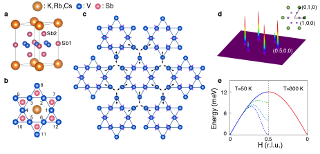
Figures 1a and b show the crystal structure of AV3Sb5, which has a space group No. 191 (P6/mmm). The V-Sb slab interlaces with the alkali triangle network along the crystal -axis. Structurally, there are two Sb positions: Sb1 is located at the center of the V-hexagon and Sb2 is sitting above and below the V-triangles. Density functional theory (DFT) calculations found that the the ideal kagomé structure is energetically unstable and favors an inverse star-of-David (ISD) structure at zero temperature [12]. While the ISD distortion of the two-dimensional kagomé lattice preserves the symmetry, recent scanning tunneling spectroscopy (STS) studies found that the CDW superlattice peaks break the six-fold rotational symmetry (Fig. 1d), suggesting a chiral CDW or electronic nematicity [10, 18, 28, 29, 30, 15]. Magnetoresistence measurements also found evidence of symmetry that persists into the superconducting phase [31, 30, 15]. Moreover, as we show in Fig. 1e, unlike well-known CDW materials [32, 23, 33, 24, 25, 26, 27, 34], CDW in AV3Sb5 fails to induce acoustic phonon anomalies near the CDW wavevector, , indicating a strong commensurability effect [18]. Here we explore the CDW by numerically and analytically assessing the structural responses below in AV3Sb5. We show that the three-dimensional ISD structure yields a diffraction pattern that is consistent with x-ray scattering (XRD) and STS measurements [9, 18, 10, 18, 28, 29]. Our analysis supports a CDW in AV3Sb5 that preserves the in the kagomé-plane. However, due to the phase shift between kagomé layers, the CDW breaks the sixfold rotational symmetry, , and strongly modifies the CDW superlattice peak intensities. Finally, we show that the coupling between CDW and lattice distortion yields a weak first order phase transition [35, 21] that may be responsible for the absence of acoustic phonon anomaly in AV3Sb5 [18].
The diffraction intensity follows, , where F(Q) is the scattering amplitude. For a crystalline material, F(Q) can be formulated as:
| (1) |
where and are real and reciprocal lattice vectors, respectively. is the atomic position in the unit cell. is the total momentum transfer and is the atomic form factor, which is derived from a Fourier transformation of local density of state (see Appendix A for more details). Below , the formation of CDW distorts the high-temperature structure and gives rise to superlattice peaks at =.
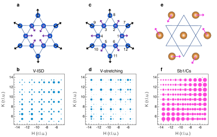
We first consider the DFT predicted ISD distortions of V-kagomé lattice. Figure 2a schematically shows the ISD distortion, where V1-6 and V7-12 are breathing out-of-phase with respect to the center of V-hexagon. Figure 2b shows the simulated diffraction pattern of ISD shown in Fig. 2a. The scattering region is chosen to match previous XRD measurement at =0 plane [9, 18], which captures in-plane atomic distortions. Remarkably, we find that ISD reproduces the key feature of experiment [9, 18], , the CDW peak intensity is significantly larger at =(, +0.5, 0) or (+0.5, , 0), than at =(, +0.5, 0) or (+0.5, , 0), where and represent even/odd integers and integers, respectively. As a comparison, we also calculate two more CDW diffraction patterns: (i) the V-stretching shown in Fig. 2c, corresponding to an in-phase breathing of V1-6 and V7-12 and preserving the symmetry; and (ii) the inversion-symmetry breaking Cs/Sb1 distortion with symmetry as shown Fig. 1e. Apparently, these lattice distortions are incompatible with the empirical selection rules and can be excluded for AV3Sb5. We shall note that the star-of-David (SD) distortion [12, 22] also captures the main feature of XRD measurement with subtle differences from ISD structure (see Appendix C). A more detailed x-ray diffraction measurement and structure refinement are required to distinguish these two patterns [12].
Since the two-dimensional ISD/SD has the symmetry, the CDW superlattice peaks are expected to show symmetry. Indeed, based on Eq. 1 and the ISD/SD distortion, we find that:
| (2) | ||||
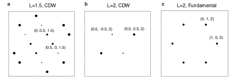
where and are corresponding to and distortions, respectively. Here we assume . This condition is justified by previous XRD measurement, where the CDW superlattice peaks are 35 orders smaller than their nearby fundamental Bragg peaks [18]. The symmetry of the CDW superlattice peak is, however, incompatible with recent STS studies, where only a symmetry is observed [10, 18, 28, 29]. As we continue to show below, when CDW is three-dimensional (3D), as reported by recent experimental studies [18, 36, 16, 21, 22], the symmetry of the CDW peak intensity naturally breaks down to . To show the rotational symmetry breaking, we use the theoretically refined 222 ISD structure of AV3Sb5 [12]. Due to the phase shift between adjacent kagomé layers, the crystal symmetry is lowered from to [7]. Figure 3a and b show the calculated CDW superlattice peak intensity at and , respectively. In agreement with STS studies [18, 36, 16, 21, 22], the CDW superlattice peak intensity only shows symmetry. In contrast, the fundamental Bragg peak only weakly breaks the symmetry due to small lattice distortions. We note that in our simulation, the fundamental Bragg peak intensity is three-orders larger than the CDW peak intensity.
Theoretically, three types of CDW order parameters are predicted for AV3Sb5, the onsite CDW, bond CDW and imaginary bond CDW involving flux or loop currents [4, 37, 5, 36, 7]. Due to finite electron-phonon coupling, CDW patterns have to respect the point group symmetry of the lattice. For instance, the Sb/Cs1 distortion shown in Fig. 2e is derived from an onsite CDW with symmetry [37]. Our simulations demonstrate that the DFT calculated 222 superstructure at zero temperature is consistent with experimental observations and therefore support a CDW with symmetry in the kagomé plane. Furthermore, as we shown in Fig. 2a-d, the anti-phase breathing of V1-6 and V7-12 puts another constraint on the CDW pattern in AV3Sb5 [37]. Our results, however, do not explain the observed chiral CDW peak intensity in AV3Sb5 [10]. Indeed, the chiral CDW keeps the symmetry of the kagomé plane [4] and hence cannot be distinguished by non-resonant x-ray scattering. Instead, the V -edge resonant x-ray scattering, which selectively enhance electronic excitions from V -orbital, might be a sensitive probe for this novel electronic order parameter [38].
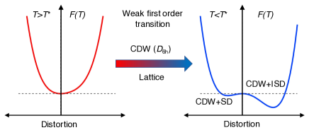
Finally we explore how lattice distortion intertwines with the CDW transition. Previous DFT calculations [12] found that the lattice energy is asymmetric with respect to the lattice distortion, , at zero temperature (Fig. 4). Since CDW always couples with lattice distortions through finite electron-phonon coupling, the asymmetric lattice-distortion energy adds a cubic term in the CDW free energy and leads to a weak first order phase transition. To elaborate it further, we consider an Ising-type Landau free energy on a two-dimensional kagomé lattice:
| (3) |
where . Note the linear term in Eq. 3 can be removed by a linear transformation of . is the CDW gap in single particle spectral function. is a constant that is proportional to the electron-phonon coupling strength. The hysteresis of the first order phase transition is, . Experimentally, 1 K [21, 35], suggesting a weak electron phonon coupling in AV3Sb5. Indeed, the calculated electron-phonon coupling constant from ref. [12] is in the weak coupling regime and between 0.30.46 for AV3Sb5, supporting our conclusion. Due to the weak first order phase transition, the change of the lattice dynamics is discontinuous near and possibly intervenes the softening of the CDW phason mode. Together with the strong commensuratbility effect of the 222 CDW, the phason gap may remain large above and failed to yield acoustic phonon softening near the CDW wavevector [18].
In summary, we explored the intricate interplay between lattice geometry and CDW in kagomé metal AV3Sb5. We prove that the ISD distortion reproduces the XRD and STS measurements. We showed that the coupling between lattice distortions and CDW induces a weak first order transition without continuous phonon softening in AV3Sb5.
Acknowledgements: We thank Kun Jiang for stimulating discussion on the interplay between CDW patterns and lattice distortions.This research was sponsored by the U.S. Department of Energy, Office of Science, Basic Energy Sciences, Materials Sciences and Engineering Division and by the Laboratory Directed Research and Development Program of Oak Ridge National Laboratory, managed by UT-Battelle, LLC, for the U. S. Department of Energy. H.C.L. was supported by National Natural Science Foundation of China (Grant No. 11822412 and 11774423), Ministry of Science and Technology of China (Grant No. 2018YFE0202600 and 2016YFA0300504) and Beijing Natural Science Foundation (Grant No. Z200005). Z.Q.W is supported by the U.S. Department of Energy, Basic Energy Sciences Grant No. DE-FG02-99ER45747. B.Y. acknowledges the financial support by the Willner Family Leadership Institute for the Weizmann Institute of Science, the Benoziyo Endowment Fund for the Advancement of Science, Ruth and Herman Albert Scholars Program for New Scientists, the European Research Council (ERC) under the European Union’s Horizon 2020 research and innovation programme (Grant No. 815869) and ISF MAFAT Quantum Science and Technology (2074/19).
Appendix A Atomic structure factor
The atomic form factor is a Fourier transform of a spatial density distribution of the scattering object. It is defined as:
| (4) |
where is the real space electron density. For non-resonant x-ray scattering, the atomic form factor is well approximated by a sum of Gaussians of the form:
Appendix B Structural domain
We consider the 222 superstructure which involves a -phase shift between the ISD distorted kagomé layers. Assuming the scattering pattern of the two-dimensional ISD structure is , the scattering intensity of 222 can be written as:
| (7) |
where (1, 0, 1) or (0, 1, 1) or (1, -1, 1) in the high temperature reciprocal lattice unit. For a measurement in a single structural domain, such as STS, Eq. 8 post strong selection rule. For instance, take (1, 0, 1), the CDW peak at (0.5, 0, 0) is actually forbidden. For a measurement that covers multiple domains, such x-ray measurement:
| (8) | ||||
Therefore, the CDW superlattice peaks determined by maulti-domain measurements will be similar to the 22 CDW.
Appendix C Star-of-David distortion
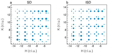
Figure 5 compares diffraction patterns of SD and ISD distortions. While the both distortions capture the empirical diffraction selection rules, SD and ISD show subtle differences, for instance, the relative intensity between (H, 13.5, 0) and (H, 12.5 0) are opposite for SD and ISD.
References
- Syôzi [1951] I. Syôzi, Statistics of Kagomé Lattice, Progress of Theoretical Physics 6, 306 (1951), https://academic.oup.com/ptp/article-pdf/6/3/306/5239621/6-3-306.pdf .
- Wang et al. [2013] W.-S. Wang, Z.-Z. Li, Y.-Y. Xiang, and Q.-H. Wang, Competing electronic orders on kagome lattices at van hove filling, Phys. Rev. B 87, 115135 (2013).
- Kiesel et al. [2013] M. L. Kiesel, C. Platt, and R. Thomale, Unconventional fermi surface instabilities in the kagome hubbard model, Phys. Rev. Lett. 110, 126405 (2013).
- Feng et al. [2021a] X. Feng, K. Jiang, Z. Wang, and J. Hu, Chiral flux phase in the kagome superconductor av3sb5 (2021a), arXiv:2103.07097 [cond-mat.supr-con] .
- Denner et al. [2021] M. M. Denner, R. Thomale, and T. Neupert, Analysis of charge order in the kagome metal v3sb5 (k,rb,cs) (2021), arXiv:2103.14045 [cond-mat.str-el] .
- Lin and Nandkishore [2021] Y.-P. Lin and R. M. Nandkishore, Complex charge density waves at van hove singularity on hexagonal lattices: Haldane-model phase diagram and potential realization in kagome metals av3sb5 (2021), arXiv:2104.02725 [cond-mat.supr-con] .
- Park et al. [2021] T. Park, M. Ye, and L. Balents, Electronic instabilities of kagome metals: saddle points and landau theory (2021), arXiv:2104.08425 [cond-mat.supr-con] .
- Ortiz et al. [2019] B. R. Ortiz, L. C. Gomes, J. R. Morey, M. Winiarski, M. Bordelon, J. S. Mangum, I. W. H. Oswald, J. A. Rodriguez-Rivera, J. R. Neilson, S. D. Wilson, E. Ertekin, T. M. McQueen, and E. S. Toberer, New kagome prototype materials: discovery of , and , Phys. Rev. Materials 3, 094407 (2019).
- Ortiz et al. [2020] B. R. Ortiz, S. M. L. Teicher, Y. Hu, J. L. Zuo, P. M. Sarte, E. C. Schueller, A. M. M. Abeykoon, M. J. Krogstad, S. Rosenkranz, R. Osborn, R. Seshadri, L. Balents, J. He, and S. D. Wilson, : A topological kagome metal with a superconducting ground state, Phys. Rev. Lett. 125, 247002 (2020).
- Jiang et al. [2021] Y.-X. Jiang, J.-X. Yin, M. M. Denner, N. Shumiya, B. R. Ortiz, G. Xu, Z. Guguchia, J. He, M. S. Hossain, X. Liu, J. Ruff, L. Kautzsch, S. S. Zhang, G. Chang, I. Belopolski, Q. Zhang, T. A. Cochran, D. Multer, M. Litskevich, Z.-J. Cheng, X. P. Yang, Z. Wang, R. Thomale, T. Neupert, S. D. Wilson, and M. Z. Hasan, Unconventional chiral charge order in kagome superconductor KV3Sb5, Nature Materials 10.1038/s41563-021-01034-y (2021).
- Yin et al. [2021] Q. Yin, Z. Tu, C. Gong, Y. Fu, S. Yan, and H. Lei, Superconductivity and normal-state properties of kagome metal rbv3sb5 single crystals, Chinese Physics Letters 38, 037403 (2021).
- Tan et al. [2021] H. Tan, Y. Liu, Z. Wang, and B. Yan, Charge density waves and electronic properties of superconducting kagome metals (2021), arXiv:2103.06325 [cond-mat.supr-con] .
- Zhao et al. [2021] H. Zhao, H. Li, B. R. Ortiz, S. M. L. Teicher, T. Park, M. Ye, Z. Wang, L. Balents, S. D. Wilson, and I. Zeljkovic, Cascade of correlated electron states in a kagome superconductor csv3sb5 (2021), arXiv:2103.03118 [cond-mat.supr-con] .
- Liang et al. [2021] Z. Liang, X. Hou, W. Ma, F. Zhang, P. Wu, Z. Zhang, F. Yu, J. J. Ying, K. Jiang, L. Shan, Z. Wang, and X. H. Chen, Three-dimensional charge density wave and robust zero-bias conductance peak inside the superconducting vortex core of a kagome superconductor csv3sb5 (2021), arXiv:2103.04760 [cond-mat.supr-con] .
- Chen et al. [2021a] H. Chen, H. Yang, B. Hu, Z. Zhao, J. Yuan, Y. Xing, G. Qian, Z. Huang, G. Li, Y. Ye, Q. Yin, C. Gong, Z. Tu, H. Lei, S. Ma, H. Zhang, S. Ni, H. Tan, C. Shen, X. Dong, B. Yan, Z. Wang, and H.-J. Gao, Roton pair density wave and unconventional strong-coupling superconductivity in a topological kagome metal (2021a), arXiv:2103.09188 [cond-mat.supr-con] .
- Yu et al. [2021] F. H. Yu, T. Wu, Z. Y. Wang, B. Lei, W. Z. Zhuo, J. J. Ying, and X. H. Chen, Concurrence of anomalous hall effect and charge density wave in a superconducting topological kagome metal (2021), arXiv:2102.10987 [cond-mat.str-el] .
- Chen et al. [2021b] K. Y. Chen, N. N. Wang, Q. W. Yin, Z. J. Tu, C. S. Gong, J. P. Sun, H. C. Lei, Y. Uwatoko, and J. G. Cheng, Double superconducting dome and triple enhancement of tc in the kagome superconductor csv3sb5 under high pressure (2021b), arXiv:2102.09328 [cond-mat.supr-con] .
- Li et al. [2021a] H. X. Li, T. T. Zhang, T. Yilmaz, Y. Y. Pai, C. Marvinney, A. Said, Q. Yin, C. Gong, Z. Tu, E. Vescovo, C. S. Nelson, R. G. Moore, S. Murakami, H. C. Lei, H. N. Lee, B. Lawrie, and H. Miao, Observation of unconventional charge density wave without acoustic phonon anomaly in kagome superconductors av3sb5 (a=rb,cs) (2021a), arXiv:2103.09769 [cond-mat.supr-con] .
- Zhou et al. [2021] X. Zhou, Y. Li, X. Fan, J. Hao, Y. Dai, Z. Wang, Y. Yao, and H.-H. Wen, Origin of the charge density wave in the kagome metal csv3sb5 as revealed by optical spectroscopy (2021), arXiv:2104.01015 [cond-mat.supr-con] .
- Wang et al. [2021] Z. X. Wang, Q. Wu, Q. W. Yin, Z. J. Tu, C. S. Gong, T. Lin, Q. M. Liu, L. Y. Shi, S. J. Zhang, D. Wu, H. C. Lei, T. Dong, and N. L. Wang, Unconventional charge density wave and photoinduced lattice symmetry change in kagome metal csv3sb5 probed by time-resolved spectroscopy (2021), arXiv:2105.11393 [cond-mat.supr-con] .
- D.W.Song et al. [2021] D.W.Song, L.X.Zheng, F.H.Yu, J.Li, L.P.Nie, M.Shan, D.Zhao, S.J.Li, B.L.Kang, Z.M.Wu, Y.B.Zhou, K.L.Sun, K.Liu, X.G.Luo, Z.Y.Wang, J.J.Ying, X.G.Wan, T.Wu, and X. H. Chen, Orbital ordering and fluctuations in a kagome superconductor csv3sb5 (2021), arXiv:2104.09173 [cond-mat.supr-con] .
- Ortiz et al. [2021] B. R. Ortiz, S. M. L. Teicher, L. Kautzsch, P. M. Sarte, J. P. C. Ruff, R. Seshadri, and S. D. Wilson, Fermi surface mapping and the nature of charge density wave order in the kagome superconductor csv3sb5 (2021), arXiv:2104.07230 [cond-mat.supr-con] .
- Varma and Simons [1983] C. M. Varma and A. L. Simons, Strong-coupling theory of charge-density-wave transitions, Phys. Rev. Lett. 51, 138 (1983).
- Miao et al. [2018] H. Miao, D. Ishikawa, R. Heid, M. Le Tacon, G. Fabbris, D. Meyers, G. D. Gu, A. Q. R. Baron, and M. P. M. Dean, Incommensurate phonon anomaly and the nature of charge density waves in cuprates, Phys. Rev. X 8, 011008 (2018).
- Weber et al. [2011a] F. Weber, S. Rosenkranz, J.-P. Castellan, R. Osborn, R. Hott, R. Heid, K.-P. Bohnen, T. Egami, A. H. Said, and D. Reznik, Extended phonon collapse and the origin of the charge-density wave in , Phys. Rev. Lett. 107, 107403 (2011a).
- Weber et al. [2011b] F. Weber, S. Rosenkranz, J.-P. Castellan, R. Osborn, G. Karapetrov, R. Hott, R. Heid, K.-P. Bohnen, and A. Alatas, Electron-phonon coupling and the soft phonon mode in , Phys. Rev. Lett. 107, 266401 (2011b).
- Kogar et al. [2017] A. Kogar, M. S. Rak, S. Vig, A. A. Husain, F. Flicker, Y. I. Joe, L. Venema, G. J. MacDougall, T. C. Chiang, E. Fradkin, J. van Wezel, and P. Abbamonte, Signatures of exciton condensation in a transition metal dichalcogenide, Science 358, 1314 (2017).
- Li et al. [2021b] H. Li, H. Zhao, B. R. Ortiz, T. Park, M. Ye, L. Balents, Z. Wang, S. D. Wilson, and I. Zeljkovic, Rotation symmetry breaking in the normal state of a kagome superconductor kv3sb5 (2021b), arXiv:2104.08209 [cond-mat.supr-con] .
- Shumiya et al. [2021] N. Shumiya, M. S. Hossain, J.-X. Yin, Y.-X. Jiang, B. R. Ortiz, H. Liu, Y. Shi, Q. Yin, H. Lei, S. S. Zhang, G. Chang, Q. Zhang, T. A. Cochran, D. Multer, M. Litskevich, Z.-J. Cheng, X. P. Yang, Z. Guguchia, S. D. Wilson, and M. Z. Hasan, Tunable chiral charge order in kagome superconductor rbv3sb5 (2021), arXiv:2105.00550 [cond-mat.supr-con] .
- Xiang et al. [2021] Y. Xiang, Q. Li, Y. Li, W. Xie, H. Yang, Z. Wang, Y. Yao, and H.-H. Wen, Twofold symmetry of c-axis resistivity in topological kagome superconductor csv3sb5 with in-plane rotating magnetic field (2021), arXiv:2104.06909 [cond-mat.supr-con] .
- Ni et al. [2021] S. Ni, S. Ma, Y. Zhang, J. Yuan, H. Yang, Z. Lu, N. Wang, J. Sun, Z. Zhao, D. Li, S. Liu, H. Zhang, H. Chen, K. Jin, J. Cheng, L. Yu, F. Zhou, X. Dong, J. Hu, H.-J. Gao, and Z. Zhao, Anisotropic Superconducting Properties of Kagome Metal {CsV}3Sb5, Chinese Physics Letters 38, 57403 (2021).
- Rice and Scott [1975] T. M. Rice and G. K. Scott, New mechanism for a charge-density-wave instability, Phys. Rev. Lett. 35, 120 (1975).
- Hoesch et al. [2009] M. Hoesch, A. Bosak, D. Chernyshov, H. Berger, and M. Krisch, Giant kohn anomaly and the phase transition in charge density wave , Phys. Rev. Lett. 102, 086402 (2009).
- Grüner [2018] G. Grüner, Density Waves in Solids (CRC Press, Taylor & Francis Group, Boca Raton, 2018) pp. 1–288.
- Mu et al. [2021] C. Mu, Q. Yin, Z. Tu, C. Gong, H. Lei, Z. Li, and J. Luo, s-wave superconductivity in kagome metal csv3sb5 revealed by 121/123sb nqr and 51v nmr measurement (2021), arXiv:2104.06698 [cond-mat.supr-con] .
- Ratcliff et al. [2021] N. Ratcliff, L. Hallett, B. R. Ortiz, S. D. Wilson, and J. W. Harter, Coherent phonon spectroscopy and interlayer modulation of charge density wave order in the kagome metals csv3sb5 (2021), arXiv:2104.10138 [cond-mat.supr-con] .
- Feng et al. [2021b] X. Feng, Y. Zhang, K. Jiang, and J. Hu, Low-energy effective theory and symmetry classification of flux phases on kagome lattice (2021b), arXiv:2106.04395 [cond-mat.supr-con] .
- Achkar et al. [2016] A. J. Achkar, M. Zwiebler, C. Mcmahon, F. He, R. Sutarto, I. Djianto, Z. Hao, G. D. Gu, A. Revcolevschi, H. Zhang, Y. Kim, J. Geck, and D. G. Hawthorn, Nematicity in stripe ordered cuprates probed via resonant x-ray scattering, Science 351, 1 (2016).
- Brown et al. [2006] P. J. Brown, A. G. Fox, E. N. Maslen, M. A. O’Keefe, and B. T. M. Willis, Intensity of diffracted intensities, International Tables for Crystallography C, 554 (2006).