Molecular beam epitaxy of single-crystalline bixbyite (In1-xGax)2O3 films (x0.18): Structural properties and consequences of compositional inhomogeneity
Abstract
In this work, we show the heteroepitaxial growth of single-crystalline bixbyite (In1-xGax)2O3 films on (111)-oriented yttria-stabilized zirconia substrates using plasma-assisted molecular beam epitaxy under various growth conditions. A pure In2O3 buffer layer between the substrate and (In1-xGax)2O3 alloy is shown to result in smoother film surfaces and significantly improved crystallinity. Symmetric out-of-plane x-ray diffraction scans show a single (111) crystal orientation and transmission electron microscopy confirms the single-crystallinity up to and only slight film quality deterioration with increasing Ga content. Partially relaxed layers are demonstrated via reciprocal space mapping with lattice parameters fitting well to Vegard’s law. However, the Ga cations are not evenly distributed within the films containing nominally : inclusions with high Ga density up to are observed within a "matrix" with . The cubic bixbyite phase is preserved, in both the "matrix" and the inclusions. Moreover, for , both the Raman phonon lines as well as the optical absorption onset remain nearly constant. Hard x-ray photoelectron spectroscopy measurements also indicate a widening of the band gap and exhibit similar saturation of the Ga 2p core level position for high Ga contents. This saturation behavior of the spectroscopic properties further supports the limited Ga incorporation into the "matrix" of the film.
I Introduction
The group-III sesquioxides In2O3 and Ga2O3 are transparent semiconducting materials widely studied both for their implementation in electronic devices and—from a fundamental semiconductor physics perspective—for their unique properties. Although these two oxide compounds are isovalent and have the same chemical configuration, the equilibrium structures of In2O3 and Ga2O3 are very different, which can be explained in terms of Coulomb and orbital interactions, influenced by cation size and valence electron energies respectively.(Ma and Wei, 2015)
On the one hand, In2O3 has a stable cubic bixbyite crystal structure and belongs to the space group 206 () with a lattice parameter of ,(Marezio, 1966) as well as a less-studied metastable rhombohedral structure of the space group 167 (). Bixbyite In2O3 possesses an optically forbidden direct band gap of approximately 2.7–2.9 eV, with strong optical absorption occurring from valence bands nearly 1 eV below the valence band maximum (VBM),(Walsh et al., 2008; King et al., 2009; Irmscher et al., 2014) resulting in an onset of strong optical absorption at around 3.7 eV. This property of In2O3 renders it transparent in the visible regime and is remarkably combined with high electrical conductivity; as In2O3 exhibits inherent n-type conductivity, due to what is commonly referred to as unintentional doping. This unintentional conductivity can be significantly enhanced by intentional donor doping. Sn-doped In2O3—commonly known as indium-tin oxide (ITO)(Chae, 2001; Tiwari et al., 2004; Tsai et al., 2016)—is the most widely commercially used transparent conducting oxide (TCO), as a transparent contact in optoelectronics, such as displays, light-emitting diodes, and solar cells.
On the other hand, Ga2O3, which has been under the spotlight for the past few years, attracting interest for applications in ultraviolet (UV) photodetectors and high-power devices. It has several polymorphs,(Roy et al., 1952; Galazka, 2018) the most stable out of which is its -phase. -Ga2O3 has a monoclinic crystal structure, which belongs to the space group 12 (C2/m), and possesses a band gap of approximately 4.8 eV.(Matsumoto et al., 1974) It is, thus, transparent within both the visible and well into the UV range. A bixbyite “”-Ga2O3 phase has been theoretically predicted to have a lattice parameter of approximately (Peelaers et al., 2015; Yoshioka et al., 2007) and a band gap of 5.0 eV, according to the latest report.(Peelaers et al., 2015) To our knowledge, this phase has not been experimentally demonstrated yet,(Playford et al., 2013) despite the early reports of Roy et al. (. 1952) Finally, contrary to In2O3, high-quality, pure Ga2O3 films are insulating at room temperature.(Wong et al., 2016)
A combination of these two oxides allows for adjustments of the properties of the two original compounds and can, for instance, facilitate band gap engineering,(Hill, 1974) as observed in other semiconductor systems. Moreover, concerning potential applications, the incorporation of Ga in the In2O3 crystal lattice would potentially provide us with a wide-band-gap TCO, assuming that additional doping with Sn can be achieved. Several studies have been done towards this direction, with films prepared by various techniques covering the entire composition range of (In1-xGax)2O3,(Kokubun et al., 2010) though most of the works found in the literature focus on the high-x, Ga-rich end.(Vasyltsiv et al., 1996; Oshima and Fujita, 2008; kranert_2014; Baldini et al., 2015) Due to the different crystal structures of the parent materials, structural changes over the composition range are expected, which should limit their miscibility and affect the electronic properties of the resulting alloy. Density-functional theory calculations estimate that the miscibility gap opens at for free-standing (In1-xGax)2O3 and at for the bixbyite alloy grown epitaxially on In2O3, independent of the growth temperature.(Maccioni et al., 2016) The recent work of Wouters et al. (2020) predicts the cubic phase to be stable up to approximately . Previous experimental investigations on (In1-xGax)2O3 polycrystalline ceramic alloys(Regoutz et al., 2015) identify the solubility limit of Ga at approximately , but, surprisingly, report a decrease of the In2O3 band gap with Ga content. Another preceding experimental study on films grown by metalorganic chemical vapor deposition(Kong et al., 2010) demonstrates a bixbyite phase for Ga contents up to and a shift of the optical absorption edge towards shorter wavelengths, which indicates a widening of the band gap. However, it is unclear whether the films are homogeneous or even contain amorphous regions. Recently Swallow et al. (2021) have clearly demonstrated valence band edge shift away from the Fermi level, increase in optical gap, and depletion of surface space charge with increasing Ga content in textured (In1-xGax)2O3 films grown by pulsed layer deposition. Nagata et al. (2020) also recently published a combinatorial thin film synthesis study showing single-crystalline bixbyite (In1-xGax)2O3 layers with a low Ga composition. Nonetheless, there is still a lack of literature with detailed structural information on well-defined high-quality (In1-xGax)2O3 films with low allowing for deep exploration of the fundamental physical properties of the bixbyite phase of this alloy.
In this work, we synthesize single-crystalline phase-pure thin (In1-xGax)2O3 films up to using plasma-assisted molecular beam epitaxy (PA-MBE) and investigate the effect of a pure In2O3 buffer layer and substrate temperature—especially during nucleation—on the film quality. The resulting films are evaluated in terms of crystallinity, lattice parameter, compositional homogeneity, optical band gap, and Raman phonon modes shift with Ga content.
II Experimental details
Substrate choice and preparation
For the purposes of this study, high quality (111)-oriented single-crystalline (In1-xGax)2O3 films have been synthesized by PA-MBE on quarters of 2-in. insulating ZrO2:Y (YSZ) (111) substrates. The study focuses on the low-x bixbyite phase end of (In1-xGax)2O3, hence the substrate choice is based on its suitability for heteroepitaxy of pure In2O3. Along the [100] direction In2O3 crystallizes on a YSZ unit cell with a cube-on-cube epitaxial relation(Tarsa et al., 1993) with a low tensile mismatch of 1.6-1.7 %,(Cowley et al., 2010; Bierwagen et al., 2009) as In2O3 has a lattice constant of 10.117 Å(Marezio, 1966)—slightly smaller than twice that of YSZ, for a Y concentration of 10 mol%(Hayashi et al., 2005) (as the ones used in this study), which amounts to approximately 10.28 Å. The choice to grow the (111) surface of In2O3 was based on the fact that the (111) plane has the lowest surface tension, i.e., surface free energy per unit area, compared to the other low-index surfaces of In2O3,(Ágoston and Albe, 2011) which facilitates the growth of smooth, unfaceted films.(Bierwagen et al., 2016) Prior to loading into the PA-MBE system, the substrates were cleaned in an ultrasonic bath with organic solvents (butyl acetate, acetone, and isopropanol for 5 minutes in each) and, finally, rinsed off with deionized water. In addition, the substrates were thermally cleaned in the MBE growth chamber at for 10 min under a high oxygen plasma flux of 1 standard cubic centimeter per minute (SCCM). The power of the oxygen plasma source (6N purity) was maintained at 300 W throughout both the annealing and growth procedures.
Film growth and in-situ film characterization
Table 1 summarizes the growth parameters used for the growth of the samples investigated in this study.
| Series | Sample | O-flux | BEPIn | BEPGa | BEPSn | In2O3 | |||||||||
| ( ) | ( ) | ( ) | (s) | (s) | (SCCM) | ( mbar) | ( mbar) | ( mbar) | (nm) | (cat.) | buffer | (nm) | (°) | ||
| I | a | 600 | 750 | 750 | 270 | 2400 | 0.5 | — | — | 294 | — | — | 2.3 | 0.23 | |
| b | — | 294 | 0.12 | no | 27 | 2.70 | |||||||||
| c | — | 267 | 0.12 | yes | 19 | 0.35 | |||||||||
| II | a | 600 | 750 | 600 | 270 | 2400 | 0.5 | — | — | 326 | — | — | 1.8 | 0.31 | |
| b | — | 312 | 0.11 | yes | 6.4 | 0.50 | |||||||||
| c | — | 375 | 0.14 | yes | 8.6 | 0.36 | |||||||||
| d | — | 356 | 0.18 | yes | 11 | 0.55 | |||||||||
| III | a | 500 | 650 | 600 | 300 | 2400 | 1.0 [3.0] | 5.3 | — | — | 647 | — | — | 1.6 | 0.23 |
| b | — | 667 | 0.05 | yes | 1.7 | 0.19 | |||||||||
| c | — | 703 | 0.08 | yes | 2.0 | 0.31 | |||||||||
| d | — | 638 | 0.10 | yes | 2.5 | 0.32 | |||||||||
| e | 1.9 | 664 | 0.08 | yes | 7.9 | 0.27 |
The oxygen fluxes of 0.5 SCCM (sample series I and II) or 1.0 SCCM (sample series III), according to Ref. Vogt and Bierwagen, 2015 correspond to activated oxygen fluxes that can provide growth rates of and , respectively, under stoichiometric growth conditions. The In cell (7N purity) temperature was kept at approximately (I and II) and (III) providing beam equivalent pressures (BEPs) around , whereas the Ga cell (7N purity) temperature was varied, so as to provide samples with different Ga cation concentrations. One Sn-doped (IGTO) film, III.e, was grown using an additional Sn flux with , as seen in Table 1. The metal fluxes limited the growth rate of the films to approximately (I and II) to (III), hence the film development was realized within the O-rich regime. The substrate was continuously rotated around its normal axis during the entire growth process at 2 rotations/min in order to result in films with a homogeneous thickness distribution.
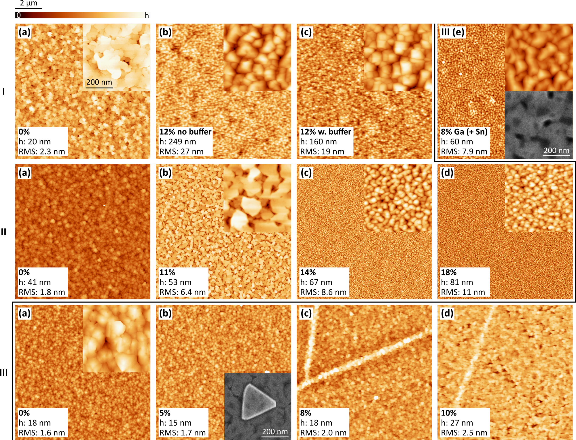
Three separate sample series were synthesized at different combinations of nucleation and film growth substrate temperatures—measured by a thermocouple between the substrate heater and the substrate, as well as different oxygen fluxes, as indicated in Table 1. Sample series I was realized with the intention to probe the effect of an approximately 40 nm thick pure In2O3 buffer layer—which also acted as a nucleation layer—between the substrate and (In1-xGax)2O3 films, as it was suspected to improve the crystalline quality of the alloy films. Series II and III were both grown using a buffer layer (approximately 40 nm and 80 nm thick respectively), based on the findings examined in the results section III.A. Inspired by the work of Franceschi et al. (, 2019) the growth was interrupted after the nucleation of the buffer layer and the substrate was heated up to as indicated in Table 1 to provide films with an enhanced smoothness. The samples of series (III), in particular, were additionally exposed to an increased O-flux of 3 SCCM during this interruption. Once was reached, the sample remained under these conditions for 10 min, before the substrate was cooled down to the final growth temperature, .
After the completion of the growth process, the samples were cooled down to room temperature in vacuum. All heat-up and cool-down processes were performed under a slow rate of to avoid film delamination. Throughout the entire growth process, the growth rate was probed by means of laser reflectometry (LR). The resulting film thicknesses from the total growth time and LR growth rate match very well those obtained by cross-sectional scanning electron microscope (SEM) imaging performed later, as specified in Table 1.
Ex-situ film investigations
Post-growth energy dispersive X-ray spectroscopy (EDX) measurements were carried out on the films with a low magnification so as to identify their average Ga composition. These were performed using an EDAX Octane Elect detector with a SDD chip mounted to a Zeiss Ultra55 scanning electron microscope operated at 7 kV. Standardless quantification using the PhiZAF routine of the EDAX-Genesis software revealed the percentage of Ga cations that ultimately got incorporated in the films assuming an oxygen content corresponding to stoichiometry. The In2O3 buffer layer could be neglected in the composition analysis because of the sufficiently large film thickness.
Out-of-plane X-ray diffraction (XRD) scans and rocking curves (ω scans) were performed within a PANalytical X’Pert Pro MRD to determine the phase purity and crystalline quality of the layers. A radiation wavelength —corresponding to a photon energy of —and a incident-beam slit and receiving slit were used for the measurements. Apart from these out-of-plane scans, reciprocal space mapping (RSM) of the (In1-xGax)2O3 844-reflex in a grazing exit alignment was employed to gauge the degree of relaxation of the films and extract their relaxed lattice parameters. Moreover, the surface morphology of the films was characterized by atomic force microscopy in the peak-force tapping mode of a Bruker Dimension Edge AFM system with ScanAsyst.
In order to evaluate the single-crystallinity of the films, transmission electron microscopy (TEM) measurements were performed with a FEI Titan 80 300 operating at 300 kV and equipped with a high annular dark field detector (HAADF). Additionally, local EDX data was simultaneously acquired using a Jeol JEM2200FS TEM at a voltage of 200 kV with an LN2 free energy dispersive X-ray SD detector to estimate the Ga incorporation on the nanoscale. The TEM samples were prepared in cross-sectional view along the direction of the YSZ substrate by plane-parallel polishing down to a thickness of 5 µm. For achieving electron transparency the samples were further thinned by argon ions in an Gatan PIPS system with an acceleration voltage of 3.5 kV under liquid nitrogen cooling, followed by a cleaning step where the acceleration voltage was stepwise reduced to 0.2 kV.
Raman spectroscopy measurements were performed in backscattering geometry from the surfaces of the epitaxial films to investigate the dependence of phonon frequences on the Ga content. The 325-nm (3.81 eV) line of a He-Cd laser was used for optical excitation. The incident laser light was focused by a microscope objective onto the sample surfaces. The backscattered light was collected by the same objective without analysis of its polarization, then spectrally dispersed by an 80-cm spectrograph (LabRam HR, Horiba/Jobin Yvon), and, finally, detected with a liquid-nitrogen-cooled charge-coupled device (CCD). For the temperature-dependent Raman scattering measurements, a continuous-flow cryostat (CryoVac) was used in the temperature range from 10 to 300 K.
The optical absorption onset of the alloy films was investigated by spectroscopic ellipsometry in the visible and ultraviolet spectral range (from 0.5 to 6.5 eV). The measurements were performed using a Woollam VASE equipped with an autoretarder. The ellipsometric parameters have been recorded at three angles of incidence (50°, 60°, and 70°) in order to increase the reliability of the obtained dielectric function (DF). The DF was analyzed as described in Ref. (Feneberg et al., 2016). Both numerical point-by-point fitted and model dielectric functions are obtained.
Finally, the electronic states of the bulk of the films have been investigated by hard x-ray photoelectron spectroscopy (HAXPES). HAXPES measurements were performed at room temperature at the revolver undulator beamline at BL15XU of SPring-8 using hard x-rays ().(Ueda et al., 2010) The corresponding inelastic mean free path (IMFP) of HAXPES for the In 3d core-level photoemission calculated by the Tanuma–Powell–Penn-2M(Tanuma, 2006) is . The probing depth is three times the IMFP,(Powell et al., 1999) therefore, our HAXPES measurements probe approximately below the sample surface, which can reduce the effect of surface Fermi level pinning of In2O3. A detailed description of the experimental setup of HAXPES at the beamline is described elsewhere.(Ueda, 2013) A high-resolution hemispherical electron analyzer (VG Scienta R4000) was used to detect the photoelectrons. The total energy resolutions of HAXPES was set to 240 meV. To determine the absolute binding energy, the XPES data were calibrated against the Au 4f7/2 peak () and the Fermi level of Au. Peak fitting of the XPES data was carried out using the Voigt function after subtracting the Shirley-type background using the KolXPD software.(kol, ; Shirley, 1972)
III Results and discussion
III.1 In2O3 buffer layer
Despite YSZ being the best-matched substrate for heteroepitaxy of In2O3, growth on it poses certain challenges. The growth is realized under the Volmer–Weber growth mode, where the film nucleates into separate islands, rather than wet the substrate.(Bierwagen and Speck, 2010) To create more favorable wetting conditions and force nucleation, the growth temperature of the substrate needs to be reduced for the growth of the initial few nm of the layer, which can have a negative impact on film smoothness and overall quality. Besides this, the resulting film will have a tensile mismatch of 1.6 % to the substrate.
The incorporation of Ga into the In2O3 lattice is expected to further aggravate the challenges of growth on YSZ. For example, In2O3 has a lattice constant of 10.117 Å(Marezio, 1966)—slightly smaller than twice that of the substrate YSZ, at 10.28 Å, whereas cubic Ga2O3 has a theoretically predicted lattice constant of approximately .(Peelaers et al., 2015; Yoshioka et al., 2007) A lattice mismatch of 1.6 % could already lead to the formation of lattice defects, such as dislocations or grain boundaries, to compensate for the change in lattice parameter, and hence result in films with low crystalline quality. Particularly in alloy films, this effect would be exacerbated. For example, an (In1-xGax)2O3 film with would have a lattice mismatch of up to 2.5 % to the YSZ substrate—assuming that the lattice parameter of the film decreases with x according to Vegard’s law (see next section for further explanation). This increased lattice mismatch between layer and substrate can result in additional crystal defects. One approach to circumvent this and partially release the strain, would be to not directly grow the (In,Ga)2O3 layers on top of YSZ, but rather aim for an initial nucleation of a pure In2O3 thin layer on YSZ, and then proceed with the growth of the (In,Ga)2O3 on top of it. This In2O3 buffer layer will then effectively act as a secondary substrate with a matching crystal structure to the alloy, which should aid film orientation, and, additionally, improve the nucleation conditions. Furthermore, the buffer layer allows for higher growth at temperatures and could, thus, result in a smoother film. This technique should also enhance the solubility at the low-x end, according to the calculations of Maccioni et al. (2016) on the miscibility of the alloy, where the miscibility of (In1-xGax)2O3 is enhanced in epitaxial growth upon In2O3, compared to the free-standing alloy.
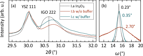
A comparison of the crystalline qualities of the films with and without a buffer layer is presented in Figure 1 based on symmetric XRD scans and corresponding rocking curves. The shift of the (In1-xGax)2O3 layer reflex towards larger angles compared to the position of the In2O3 layer reflex indicates a decrease in the lattice parameter, as expected. Evidently, a pure In2O3 buffer layer on top of YSZ results in an (In1-xGax)2O3 film with a significantly better quality compared to the one grown on top of a Ga-containing nucleation layer. This is further confirmed by the AFM images in Fig. 2, which shows that the sample grown on a buffer layer (I.c) is significantly smoother and has better defined structures than the one without the buffer (I.b). Based on this finding, all further samples grown for this study included an In2O3 buffer for improved surface smoothness and crystallinity.
III.2 Structure dependence on Ga content
Surface morphology
As In2O3 does not easily wet the YSZ substrate,(Bierwagen and Speck, 2010) the substrate temperature used for the growth of—especially—the initial few nm of the epilayer has a clear effect on its crystalline quality, which is also confirmed by the comparison of three pure In2O3 films (I.a, II.a, III.a) grown at different temperatures, in the AFM images of Fig. 2. An overall increasing roughness and density of morphological features with increasing Ga content can be observed. The average grain size decreases with Ga, in accordance with the findings of Kong et al. (. 2010) This indicates that the incorporation of Ga leads to a lower surface diffusion length. The growth temperature seemingly also affects the surface diffusion length, with lower temperatures resulting in smoother films with smaller features. However, this result is probably due to the lower nucleation temperature, which enhances wetting.
Phase purity, lattice parameter, and compositional (in)homogeneity
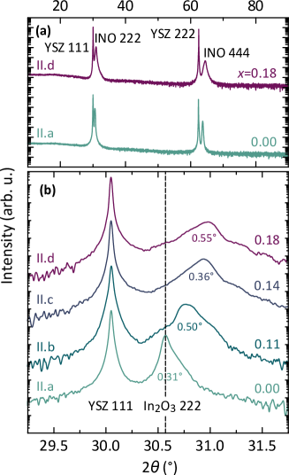
As seen in the wide range symmetric scans XRD scans in Fig. 3 (a), the film with the highest Ga content, (In0.82Ga0.18)2O3, exhibits only one pure, 111-oriented cubic phase, in contrast to earlier works on In2O3 ceramics(Regoutz et al., 2015) and nanowires(Chun et al., 2004) with comparable or even lower Ga contents, where several orientations are reported. Moreover, no secondary crystalline Ga2O3 phases are observed, in contrast to a previous investigation on films grown by PA-MBE containing higher amounts of Ga.(Vogt, 2017) The observed low full width at half maximum (FWHM) values from the rocking curves in Fig. 3 (b), , indicate high crystalline quality. However, an overall increase of the with increasing Ga content is exhibited, which would be consistent with slight deterioration of film quality. The lower intensity features on the right of the (In1-xGax)2O3 peak could point towards compositional inhomogeneity in the film, however, considering the values at which they arise, they could also be attributed to interference fringes from the high-quality thin In2O3 buffer layer at the interface.
The observed shift of the layer peak towards larger values is expected, as it reflects the decrease of lattice constant, from that of In2O3 towards the theoretically predicted one of cubic Ga2O3. Since both parent components, i.e., In2O3 and the theoretically predicted bixbyite Ga2O3, have the same crystal structure in their pure form, Vegard’s law can be applied (Eq. 1) to obtain the relaxed lattice parameter of the alloy.
| (1) |
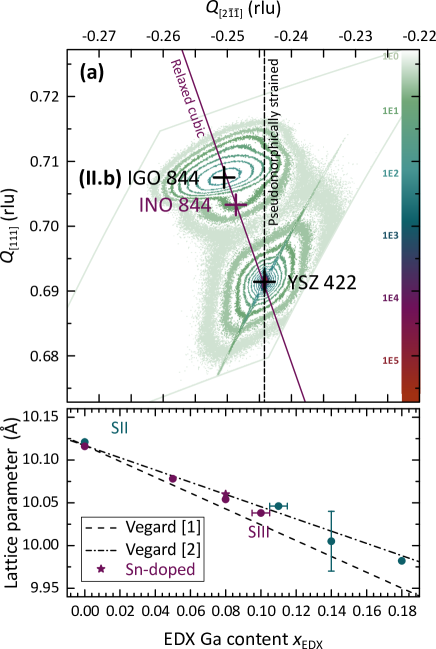
However, the peak position of measurements like those in Fig. 3 provide information only about the out-of-plane lattice parameter. In order to gain knowledge of the relaxed lattice parameter of the layers—which is affected by both in- and out-of-plane strain, RSMs have been obtained for the films of series II and III. These were performed at an asymmetrical grazing exit alignment at a range of and values that included the 4 2 2-reflex of the YSZ substrate and 8 4 4-reflex of the (In1-xGax)2O3 film. An example of such a map can be seen in Fig. 4 (a). The (4 2 2) and (8 4 4) planes can be decomposed into a component parallel and perpendicular to the lattice plane as
| (2a) |
| (2b) |
The corresponding reciprocal lattice vectors and along those two directions are
| (3) |
| (4) |
where and are the incidence and diffraction angles in radians, respectively. All cubic materials should have the same ratio of in- and out-of-plane lattice components, i.e., for a fully relaxed layer, in map plotted in terms of and such as the one in Fig. 4 (a), we would expect the (In1-xGax)2O3 844 peak to lie on the same line connecting the point and the 422 peak of the cubic YSZ substrate. For a pseudomorphically strained film, the grown film would assume the in-plane lattice parameter of the substrate, hence the in-plane component of both should be equal. Based on this, it can be concluded that the sample II.b is almost fully relaxed. The same applies to all other films grown for this study, the maps of which are not plotted here.
The in- and out-of-plane lattice spacing between adjacent (In1-xGax)2O3 lattice planes can be calculated from the and as
| (5a) | |||
| (5b) |
where is the wavelength of the x-rays. The corresponding in- and out-of-plane (In1-xGax)2O3 lattice constants are calculated using the in- and out-of-plane components of the (844) plane given by Eq. 2b and
| (6a) |
| (6b) |
accordingly. Based on the values for and extracted from the maps and the definition of the Poisson ratio(Birkholz, 2006) (Eq. 7, where are the in- and out-of-plane strain respectively), one can calculate the total relaxed lattice parameter, , whilst taking into account that in the case of a cubic crystal the in- and out-of-plane relaxed lattice parameters should be equal.
| (7) |
Here we used obtained experimentally by Zhang et al. (2011) for 111-oriented In2O3 grown on YSZ. Fig. 4 (b) shows the relaxed lattice parameters, , of the alloy films extracted from the RSM measurements as a function of Ga content, as measured by EDX. The obtained agree reasonably well with the experimental results documented in the earlier work of Regoutz et al. (2015) on (In,Ga)2O3 ceramics. The plot reveals a roughly linear dependence of the lattice constant on the alloy composition, hence, our films largely follow Vegard’s law within the margins of error. The uncertainty in is approximately 1 % for all samples and uncertainty in of sample II.c as depicted in Fig. 4 (b) is due to significant discrepancies among the various obtained RSMs. The limits posed by the two dashed lines have been calculated assuming Vegard’s law for the lattice constants of cubic bixbyite Ga2O3 reported in Refs. Peelaers et al. (2015) (9.190 Å, extracted from Fig. 3 therein) and Yoshioka et al. (2007) (9.40 Å). The agreement with Vegard’s law implies the incorporation of Ga cations on In sites and does not indicate a solubility limit within the -range studied here, that is up to . A linear fit of the lattice constant data in Fig. 4 (b) lets us estimate an experimental value for the hypothetical cubic bixbyite phase of Ga2O3 at .
Unfortunately, the low intensity and large width of the layer reflexes in the RSMs did not allow the extraction of separate and precise in- and out-of-plane lattice parameters—and therefore strains—that can be systematically explained for the samples with . This is because the relaxed lattice parameter, , is relatively less affected by the reflex position, as compared to the strain. However, comparing their In2O3 reference samples (II.a, III.a), series II seems to be less strained than series III, which was grown at lower nucleation and final substrate temperatures, with II.a showing an in-plane strain of and sample III.a . We do not expect the alloy films to be significantly more strained and presume an upper strain limit of approximately .
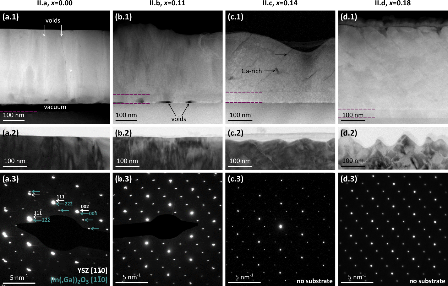
The films of sample series II have been investigated by TEM to examine their single-crystallinity and overall film quality. At the top of Fig. 5 (a.1-d.1), high angle annular dark field scanning transmission electron microscopy (HAADF-STEM) images, in which the contrast is proportional to the mean atomic number, of the four epitaxial layers are compared. The surfaces there are affected by the ion milling process, in which the sample is thinned down to electron transparency. The real growth surfaces are shown right underneath (Fig. 5 a.2-d.2) as bright field TEM images. Some voids can be observed traveling in the form of thin vertical lines through the layer for the pure In2O3 as indicated by white arrows, and as more extended regions in the film with . The films with x=0.14 and x=0.18 do not show such strong voids at the interface and surface and appear rougher with peak to valley distances of a few tens of a nm. This suggests that the addition of Ga induces a different growth mode along facets due to a destabilization of the (111) plane. Another distinct feature in samples II.c and II.d with the nominally highest Ga contents are the dark stripes traveling diagonally upward at a fixed angle through the layer. These features can be identified as regions of increased Ga incorporation according to the EDX analysis of sample II.c, as shown below (Fig. 6). The combined electron diffraction patterns of substrate and film, in Fig. 5 (a.3-d.3), show the presence of a single cubic bixbyite crystalline phase in all samples. All points can be linked to either those of the cubic structure of YSZ or those of the cubic bixbyite structure of the film. Since these lattices have similar cubic symmetry with an almost identical lattice parameter—considering a doubling of the periodicity for the bixbyite phase—some spots of the distinct phases are overlapping and have been indexed twice.
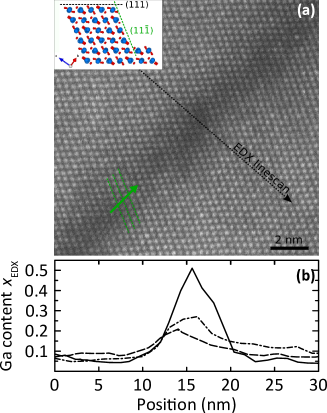
EDX point scans on sample II.b with performed in darker and brighter intensity regions of the film show Ga content fluctuations of only 1 % (not shown here). This indicates a homogeneous incorporation of the Ga cations in the cubic bixbyite lattice. However, sample II.c with exhibits areas with increased Ga contents varying from up to 0.50 compared to the surrounding “matrix”, which features an average Ga incorporation of approximately . This has been identified by EDX line scans crossing the dark features, as shown in Fig. 6 (b). One such dark stripe is imaged by HAADF-STEM at high magnification in Fig. 6 (a) in the zone axis orientation of the lattice. The bixbyite structure is preserved throughout the dark stripe without the formation of an additional phase or any lattice defects, which confirms the electron diffraction data that the layer is single-phase. The EDX line scans also show a dip in O content coinciding with the Ga increase (cf. supplement,SUP, Fig. 2 therein), indicating void formation as well. The rough surface, the void formation, and the defined orientation of the Ga-rich stripes suggests a faceted 3D island growth, with phase separation resulting from the preferential incorporation of Ga at edges of voids and on well-defined facets. The edge of preferential incorporation seems to correspond to the plane (equivalent to 111), as indicated in Fig. 6 (a), and the edge travels both laterally and vertically (in the direction of the green arrow) through the layer. Similar Ga-rich features are observed in the MBE growth of AlGaN, where enhanced Ga incorporation is observed on step edges due to a higher Ga desorption rate on the terraces.(Mayboroda et al., 2017) The sample (not shown here) exhibits similar darker stripes and defects due to relaxation processes through misfit dislocations, as well as grains and initial signs of phase separation and amorphicity, but maintains a single cubic phase throughout.
Hence, despite the preservation of the bixbyite phase and the good agreement with Vegard’s law, Ga is inhomogeneously distributed in the samples with .
Saturation of Raman phonon mode shift, (optical) absorption edge, and Ga 2p core level position
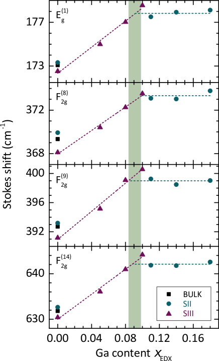
In Ref. Feldl et al., 2021 a monotonous blueshift with increasing Ga contents up to has been observed for several optical phonon modes in MBE grown (In1-xGax)2O3 films (sample series III), demonstrating that Raman spectroscopy can be a suitable tool to determine the Ga incorporation in this alloy, in the case of homogeneous Ga distribution. Figure 7 displays the frequency of such phonon modes for the samples of series II, which includes films with nominally , along with the data reported in Ref. Feldl et al., 2021. The Raman spectra of all alloy films exhibit a typical fingerprint of In2O3 phonon modes with no indication of additional phases (as in the high quality bulk crystal in Ref. Galazka et al., 2014) with no indication of additional phases. The minor discrepancies among the phonon frequencies of the binary In2O3 films of different sample series can be potentially attributed to different degrees of lattice strain. Strikingly, the frequencies of all phonon modes remain constant for nominal Ga contents above , with the saturation values of the individual phonon frequencies agreeing reasonably well with those obtained for .(Feldl et al., 2021) The absence of a further blueshift with increasing nominal Ga content is most likely related to the findings of the TEM investigations reporting a Ga incorporation of approximately in the main “matrix” of the film and inclusions with significantly higher Ga content for those films. Apparently, the Raman spectra are dominated by scattering in the “matrix” of the films and not by the total Ga content of the films. The total volume of the regions with extraordinary large Ga contents observed by TEM is most likely too small to be detected in the Raman spectra.
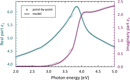
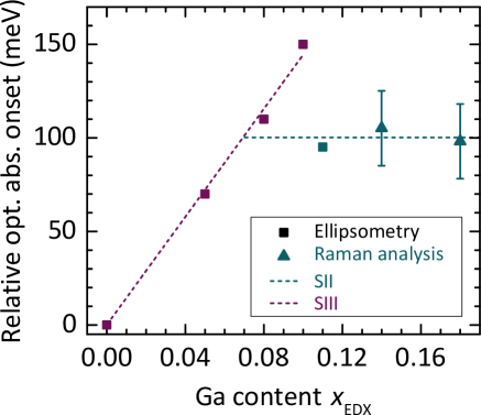
Spectroscopic ellipsometry is demonstrated in Ref. Feldl et al., 2021 to be a further spectroscopic tool to study the incorporation of Ga in (In1-xGax)2O3 alloy films. The onset of optical absorption has been shown to exhibit a pronounced blueshift with increasing Ga content for the samples of series III. Regarding sample series II, the dielectric function of the sample with is shown in Fig. 8. A comparison between the dielectric functions of the samples of series II and pure In2O3 can be found in the recent work of Feldl et al. (2021). The observed blueshift of the absorption onset by 95 meV induced by alloying is somewhat lower than expected based on the results reported in Ref. Feldl et al., 2021, presumably due to the different growth conditions. Note that many-body corrections such as the Burstein-Moss effect and band gap renormalization can be neglected for the investigated sample,(Feneberg et al., 2016) which has been annealed in oxygen (rapid thermal annealing at a final temperature of at atmospheric pressure for 60 s). Due to rough surface morphologies (see Fig. 2), samples with could not be analyzed by spectroscopic ellipsometry. Instead, we developed a method to determine the blueshift of the absorption onset in such alloy films by Raman spectroscopy. Our approach is based on the fact that the relative contribution of Raman scattering in the YSZ substrate is directly correlated with the optical absorption in the (In1-xGax)2O3 alloy films. Utilizing optical excitation at 3.81 eV (close to the onset of absorption), the intensity of the YSZ substrate signal in Raman spectra can be used to determine the alloying-induced blueshift of the optical absorption onset in those rough samples. A detailed description of our approach and a verification of its validity are presented in the Supplemental Material. The obtained relative optical absorption onsets for and are shown in Fig. 9 along with the value determined by spectroscopic ellipsometry for (see Fig. 8). In accordance with the result obtained for the frequencies of optical phonons, no clear dependence of the absorption onset on the nominal Ga content is found for within the limits of accuracy (uncertainty of about 20 meV). Consequently, the saturation of the blueshifts found for both the phonon frequencies and the optical absorption onset confirm the phase separation observed by TEM for alloy films with nominal Ga contents above about 10 %.
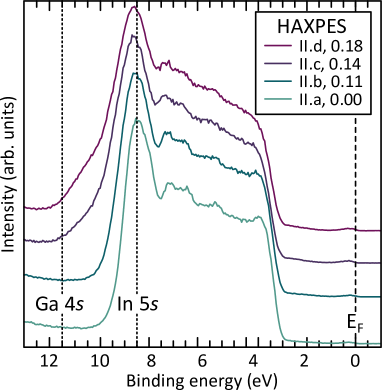
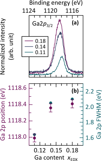
Finally, in order to investigate chemical bonding and electronic states of the alloy, the films of series II have been investigated by HAXPES. The valence band structure of three of those (II.a, b, and d) can be seen in Fig. 10. For In2O3 and Ga2O3, features around 8.5 and 11.5 eV are expected, corresponding to the In 5s and Ga 4s orbitals, respectively. As seen in Fig. 10, the addition of Ga shifts the spectrum to higher binding energies. For the II.d. film with , in particular, an additional, distinct feature can be observed at the high-binding-energy end. This could be attributed to the inclusions with very high Ga contents having distinctly different valence band structure. Charge distributions of the Ga bonding state were confirmed in the Ga 2p spectra for all Ga-containing samples of series II, as shown in Fig. 11. Both the peak position and FWHM values of Ga 2p core level change significantly for . The saturation of core level position likely reflects the “matrix” of the film, similar to the saturation observed in the Raman line frequencies shift and optical band gap width.
Hence, the investigations and analysis of the (In1-xGax)2O3 alloy films using spectroscopic techniques, along with the combination of TEM and EDX data, revealed that XRD results inferring a homogeneous incorporation of the Ga cations up to can be misleading.
IV Conclusion
The heteroepitaxial growth of (In1-xGax)2O3 on YSZ is enhanced by the employment of a thin pure In2O3 buffer layer between the alloy film and the substrate, which provides a better-matched substrate in terms of wetting, chemistry, and lattice parameter. This has been demonstrated in terms of small full widths at half maximum of x-ray diffraction rocking curves, which indicate higher film crystallinity, as well as smoother film surfaces. Both x-ray diffraction and transmission electron microscopy investigations confirm the cubic phase purity and single-crystallinity of the films up to nominal Ga contents of . Moreover, the lattice parameters of the films measured by x-ray diffraction reciprocal space mapping obey Vegard’s law, assuming the Ga contents measured by energy dispersive x-ray spectroscopy. These findings would imply a homogeneous incorporation of Ga in the alloy films.
However, closer inspection of dark features in transmission electron micrographs of the samples with the highest Ga compositions and local energy dispersive x-ray spectroscopy measurements reveal Ga containing inclusions in the films with Ga contents as high as , while the remaining film, the “matrix”, exhibits an average Ga incorporation of approximately . Nevertheless, both of these regions preserve the cubic bixbyite structure. The analysis of the (In1-xGax)2O3 alloy films by Raman spectroscopy, spectroscopic ellipsometry, and hard x-ray photoelectron spectroscopy corroborates this finding. They show systematic shifts up to an average composition of approximately and saturation for further increasing , in which case their results largely reflect the properties of the “matrix” rather than that of the average material, i.e., both the “matrix” and inclusions with high .
Thus, the observations of x-ray diffraction and reciprocal space maps can be misleading. Since the changes in lattice parameter—larger for In2O3 and smaller with increasing for (In1-xGax)2O3—happen within an elastic medium, relaxation between areas with different Ga contents takes place. An effect of “averaging” can be observed in this respect. On the contrary, this averaging effect is not visible in local microscopy investigations and spectroscopic methods that are not largely affected by strain and, thus, the larger volume of the film “matrix” is reflected within these, rather than the inclusions with high .
Acknowledgment
We would like to thank Duc Van Dinh and Thomas Teubner for critically reading this manuscript, as well as Uwe Jahn for help with the EDX investigations of the Ga content of the films, Anne-Kathrin Bluhm for the cross-sectional SEM images for film thickness characterization, and Hans-Peter Schönherr and Carsten Stemmler for technical assistance with the MBE system. This study was performed in the framework of GraFOx, a Leibniz-ScienceCampus partially funded by the Leibniz Association. We are also grateful to HiSOR, Hiroshima University, and JAEA/SPring-8 for the development of HAXPES at BL15XU of SPring-8. The HAXPES measurements were performed under the approval of the NIMS Synchrotron X-ray Station (Proposal No. 2019B4602).
References
- Ma and Wei (2015) J. Ma and S.-H. Wei, Computational Materials Science 104, 35 (2015).
- Marezio (1966) M. Marezio, Acta Crystallographica 20, 723 (1966).
- Walsh et al. (2008) A. Walsh, J. L. F. Da Silva, S.-H. Wei, C. Körber, A. Klein, L. F. J. Piper, A. DeMasi, K. E. Smith, G. Panaccione, P. Torelli, D. J. Payne, A. Bourlange, and R. G. Egdell, Phys. Rev. Lett. 100, 167402 (2008).
- King et al. (2009) P. D. C. King, T. D. Veal, F. Fuchs, C. Y. Wang, D. J. Payne, A. Bourlange, H. Zhang, G. R. Bell, V. Cimalla, O. Ambacher, R. G. Egdell, F. Bechstedt, and C. F. McConville, Phys. Rev. B 79, 205211 (2009).
- Irmscher et al. (2014) K. Irmscher, M. Naumann, M. Pietsch, Z. Galazka, R. Uecker, T. Schulz, R. Schewski, M. Albrecht, and R. Fornari, Phys. Status Solidi A 211, 54 (2014).
- Chae (2001) G. S. Chae, Jpn. J. Appl. Phys. 40, 1282 (2001).
- Tiwari et al. (2004) A. N. Tiwari, G. Khrypunov, F. Kurdzesau, D. L. Bätzner, A. Romeo, and H. Zogg, Prog. Photov. 12, 33 (2004).
- Tsai et al. (2016) M. Y. Tsai, O. Bierwagen, and J. S. Speck, Thin Solid Films 605, 186 (2016).
- Roy et al. (1952) R. Roy, V. G. Hill, and E. F. Osborn, Journal of the American Chemical Society 74, 719 (1952).
- Galazka (2018) Z. Galazka, Semiconductor Science and Technology 33, 113001 (2018).
- Matsumoto et al. (1974) T. Matsumoto, M. Aoki, A. Kinoshita, and T. Aono, Japanese Journal of Applied Physics 13, 1578 (1974).
- Peelaers et al. (2015) H. Peelaers, D. Steiauf, J. B. Varley, A. Janotti, and C. G. Van de Walle, Phys. Rev. B 92, 085206 (2015).
- Yoshioka et al. (2007) S. Yoshioka, H. Hayashi, A. Kuwabara, F. Oba, K. Matsunaga, and I. Tanaka, Journal of Physics: Condensed Matter 19, 346211 (2007).
- Playford et al. (2013) H. Y. Playford, A. C. Hannon, E. R. Barney, and R. I. Walton, Chemistry—A European Journal 19, 2803 (2013).
- Wong et al. (2016) M. H. Wong, K. Sasaki, A. Kuramata, S. Yamakoshi, and M. Higashiwaki, Japanese Journal of Applied Physics 55, 1202B9 (2016).
- Hill (1974) R. Hill, Journal of Physics C: Solid State Physics 7, 521 (1974).
- Kokubun et al. (2010) Y. Kokubun, T. Abe, and S. Nakagomi, physica status solidi (a) 207, 1741 (2010).
- Vasyltsiv et al. (1996) V. I. Vasyltsiv, Y. I. Rym, and Y. M. Zakharko, Physica Status Solidi B: Basic Solid State Physics 195, 653 (1996).
- Oshima and Fujita (2008) T. Oshima and S. Fujita, physica status solidi c 5, 3113 (2008).
- Baldini et al. (2015) M. Baldini, M. Albrecht, D. Gogova, R. Schewski, and G. Wagner, Semiconductor Science and Technology 30, 024013 (2015).
- Maccioni et al. (2016) M. B. Maccioni, F. Ricci, and V. Fiorentini, Journal of Physics: Condensed Matter 28, 224001 (2016).
- Wouters et al. (2020) C. Wouters, C. Sutton, L. M. Ghiringhelli, T. Markurt, R. Schewski, A. Hassa, H. von Wenckstern, M. Grundmann, M. Scheffler, and M. Albrecht, Phys. Rev. Materials 4, 125001 (2020).
- Regoutz et al. (2015) A. Regoutz, R. Egdell, D. Morgan, R. Palgrave, H. Téllez, S. Skinner, D. Payne, G. Watson, and D. Scanlon, Applied Surface Science 349, 970 (2015).
- Kong et al. (2010) L. Kong, J. Ma, F. Yang, C. Luan, and Z. Zhu, Journal of Alloys and Compounds 499, 75 (2010).
- Swallow et al. (2021) J. E. N. Swallow, R. G. Palgrave, P. A. E. Murgatroyd, A. Regoutz, M. Lorenz, A. Hassa, M. Grundmann, H. von Wenckstern, J. B. Varley, and T. D. Veal, ACS Applied Materials & Interfaces 13, 2807 (2021).
- Nagata et al. (2020) T. Nagata, T. Hoga, A. Yamashita, T. Asahi, S. Yagyu, and T. Chikyow, ACS Combinatorial Science 22, 433 (2020).
- Tarsa et al. (1993) E. J. Tarsa, J. H. English, and J. S. Speck, Appl. Phys. Lett. 62, 2332 (1993).
- Cowley et al. (2010) R. A. Cowley, A. Bourlange, J. L. Hutchison, K. H. L. Zhang, A. M. Korsunsky, and R. G. Egdell, Phys. Rev. B 82, 165312 (2010).
- Bierwagen et al. (2009) O. Bierwagen, M. E. White, M.-Y. Tsai, and J. S. Speck, Applied Physics Letters 95, 262105 (2009).
- Hayashi et al. (2005) H. Hayashi, T. Saitou, N. Maruyama, H. Inaba, K. Kawamura, and M. Mori, Solid State Ionics 176, 613 (2005).
- Ágoston and Albe (2011) P. Ágoston and K. Albe, Phys. Rev. B 84, 045311 (2011).
- Bierwagen et al. (2016) O. Bierwagen, J. Rombach, and J. S. Speck, Journal of Physics: Condensed Matter 28, 224006 (2016).
- Vogt and Bierwagen (2015) P. Vogt and O. Bierwagen, Appl. Phys. Lett. 106, 081910 (2015).
- Franceschi et al. (2019) G. Franceschi, M. Wagner, J. Hofinger, T. c. v. Krajňák, M. Schmid, U. Diebold, and M. Riva, Phys. Rev. Materials 3, 103403 (2019).
- Feneberg et al. (2016) M. Feneberg, J. Nixdorf, C. Lidig, R. Goldhahn, Z. Galazka, O. Bierwagen, and J. S. Speck, Physical Review B 93, 045203 (2016).
- Ueda et al. (2010) S. Ueda, Y. Katsuya, M. Tanaka, H. Yoshikawa, Y. Yamashita, S. Ishimaru, Y. Matsushita, and K. Kobayashi, AIP Conference Proceedings 1234, 403 (2010).
- Tanuma (2006) S. Tanuma, J. Surf. Sci. Soc. Japan. 27, 657 (2006).
- Powell et al. (1999) C. Powell, A. Jablonski, I. Tilinin, S. Tanuma, and D. Penn, Journal of Electron Spectroscopy and Related Phenomena 98-99, 1 (1999).
- Ueda (2013) S. Ueda, Journal of Electron Spectroscopy and Related Phenomena 190, 235 (2013).
- (40) https://www.kolibrik.net/en/kolxpd .
- Shirley (1972) D. A. Shirley, Phys. Rev. B 5, 4709 (1972).
- Bierwagen and Speck (2010) O. Bierwagen and J. S. Speck, Journal of Applied Physics 107, 113519 (2010).
- Chun et al. (2004) H. J. Chun, Y. S. Choi, S. Y. Bae, H. C. Choi, and J. Park, Applied Physics Letters 85, 461 (2004).
- Vogt (2017) P. Vogt, Growth Kinetics, Thermodynamics, and Phase Formation of group-III and IV oxides during Molecular Beam Epitaxy, Ph.D. thesis, Mathematisch-Naturwissenschaftliche Fakultät, Humboldt-Universität zu Berlin (2017).
- Birkholz (2006) M. Birkholz, Thin Film Analysis by X-ray Scattering (Wiley-VCH, Weinheim, Germany, 2006).
- Zhang et al. (2011) K. H. L. Zhang, A. Regoutz, R. G. Palgrave, D. J. Payne, R. G. Egdell, A. Walsh, S. P. Collins, D. Wermeille, and R. A. Cowley, Phys. Rev. B 84, 233301 (2011).
- (47) “See supplemental material at [url] for additional information.” .
- Mayboroda et al. (2017) I. O. Mayboroda, A. A. Knizhnik, Y. V. Grishchenko, I. S. Ezubchenko, M. L. Zanaveskin, O. A. Kondratev, M. Y. Presniakov, B. V. Potapkin, and V. A. Ilyin, Journal of Applied Physics 122, 105305 (2017).
- Feldl et al. (2021) J. Feldl, M. Feneberg, A. Papadogianni, J. Lähnemann, T. Nagata, O. Bierwagen, R. Goldhahn, and M. Ramsteiner, arXiv:2104.08092 (2021).
- Galazka et al. (2014) Z. Galazka, R. Uecker, and R. Fornari, Journal of Crystal Growth 388, 61 (2014).