Graphene FET on diamond for high-frequency electronics
Abstract
Transistors operating at high frequencies are the basic building blocks of millimeter-wave communication and sensor systems. The high charge-carrier mobility and saturation velocity in graphene can open way for ultra-fast field-effect transistors with a performance even better than what can be achieved with III-V-based semiconductors. However, the progress of high-speed graphene transistors has been hampered by fabrication issues, influence of adjacent materials, and self-heating effects. Here, we report on the improved performance of graphene field-effect transistors (GFETs) obtained by using a diamond substrate. An extrinsic maximum frequency of oscillation of up to 54 GHz was obtained for a gate length of 500 nm. Furthermore, the high thermal conductivity of diamond provides an efficient heat-sink, and the relatively high optical phonon energy of diamond contributes to an increased charge-carrier saturation velocity in the graphene channel. Moreover, we show that GFETs on diamond exhibit excellent scaling behavior for different gate lengths. These results promise that the GFET-on-diamond technology has the potential of reaching sub-terahertz frequency performance.
Diamond, field-effect transistors, graphene, maximum frequency of oscillation, MOGFETs, optical phonons, saturation velocity, transit frequency.
1 Introduction
Graphene is a 2D material with unique electrical properties such as extremely high charge-carrier velocity useful for transit types of devices [1]. There has been extensive research and progress on high-frequency graphene electronics since the first top-gated graphene field-effect transistor (GFET) was demonstrated in 2007 [2]. In 2012, excellent GFET performance with intrinsic transit frequencies above 400 GHz was achieved for a 67-nm gate length GFET [3]. However, this excellent performance was not matched by the maximum frequency of oscillation that lagged considerably due to non-negligible gate resistances.
In GFETs, the maximum frequency of oscillation is in part limited by poor drain current saturation which results in a non-negligible drain output conductance [4]. In 2016, an extrinsic transit frequency () of 50 GHz and a maximum oscillation frequency () of 40 GHz was achieved for a gate length of 200 nm using quasi-freestanding bilayer epitaxial graphene grown on a SiC (0001) substrate [5]. Recently, using an improved fabrication process for CVD GFETs, Bonmann et al. demonstrated an extrinsic of 34 GHz and a matching of 37 GHz for 500-nm GFETs with promising scaling behaviour [6]. In order to minimise the output conductance it is essential to minimize the number of charge carriers not induced by the field such as carriers due to contaminants and traps in the adjacent materials, or carriers induced by self-heating.
Another performance-limiting factor is the influence on the charge-carrier velocity due to optical-phonon scattering with the materials surrounding the graphene channel. Hence, surrounding materials with high optical-phonon energies are preferred since there is a direct correlation between the charge-carrier velocity and the transit frequency as confirmed by ref [7].
In this work, we utilize both the high surface optical phonon energy and the high thermal conductivity of diamond as a substrate to increase the GFET performance. A record high extrinsic of 54 GHz was achieved for a top-gated GFET on a single-crystal diamond substrate. We estimate the charge-carrier saturation velocity being as high as cm/s. Finally, we show that the high-frequency performance scales with the gate length, which indicates that GFETs on diamond have the potential of reaching sub-terahertz frequencies.
2 Methods
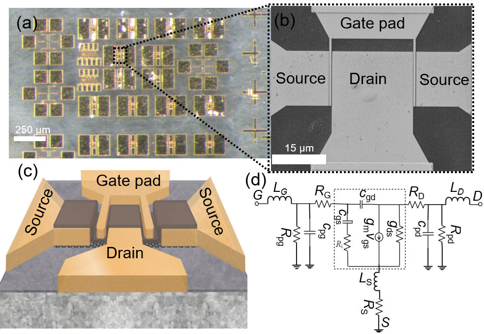
Top-gated dual-channel RF GFETs were fabricated on a high-quality free-standing single-crystal diamond substrate. The commercially available diamond substrate was homoepitaxially grown in the (100) direction using chemical vapor deposition (CVD) by Element Six Ltd [8]. Fig. 1(a) shows an optical micrograph of a set of GFETs with gate lengths () varying from 0.5 m to 2 m and a total gate width of 30 m. Fig. 1(b) shows a SEM image of a 0.5 m two-finger GFET. For illustration, Fig. 1(c) shows a three-dimensional view of the GFET layout. As a first step of the fabrication process, monolayer CVD graphene was transferred on to the diamond substrate, followed by deposition of a 5-nm thick /Ti protection layer for avoiding contact between the electron-beam resist defining the source/drain areas and the graphene. After wet-etch removal of the protection layer in the source/drain resist openings, Ti/Pd/Au (1 nm/15 nm/285 nm) was deposited and source/drain contacts were fabricated using lift-off. The use of a protection layer is important for obtaining a clean metal/graphene interface and a low contact resistance. Next, the graphene mesa was defined. After removal of the remaining protection layer from the channel area, the gate dielectric stack was formed by a 5-nm thick thermally oxidized seed layer and an 18-nm thick top layer deposited by atomic layer deposition. The gate fingers, the gate pad, and the source/drain pads were formed by deposition of a Ti/Au (100 nm/300 nm) layer. All patterns were defined using electron-beam lithography.
For GFET characterization, transfer and output characteristics were obtained using a Keithley 2612B dual-channel source meter. High-frequency -parameters were measured up to 40 GHz using an Agilent N5230A network analyzer. Two-port open-short-load-through calibration was performed using a standard calibration chip prior to the -parameter measurements. De-embedding and extraction of the small-signal equivalent-circuit elements was performed based on the method described by Dambrine et al. [9]. Special test structures were included to find the pad capacitances and inductances from the S-parameter measurements. For analysing the GFET high-frequency performance, the small-signal equivalent circuit shown in Fig. 1(d) was used.
3 Results and discussions
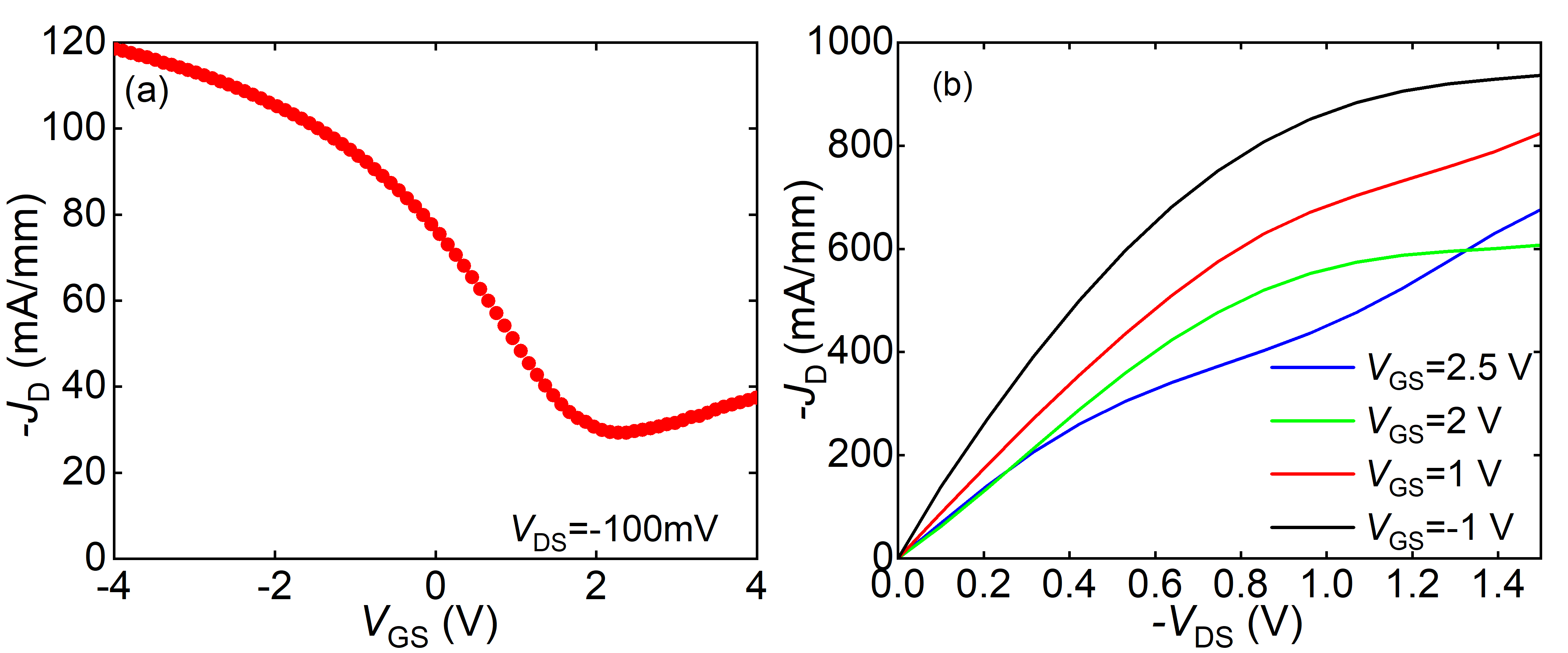
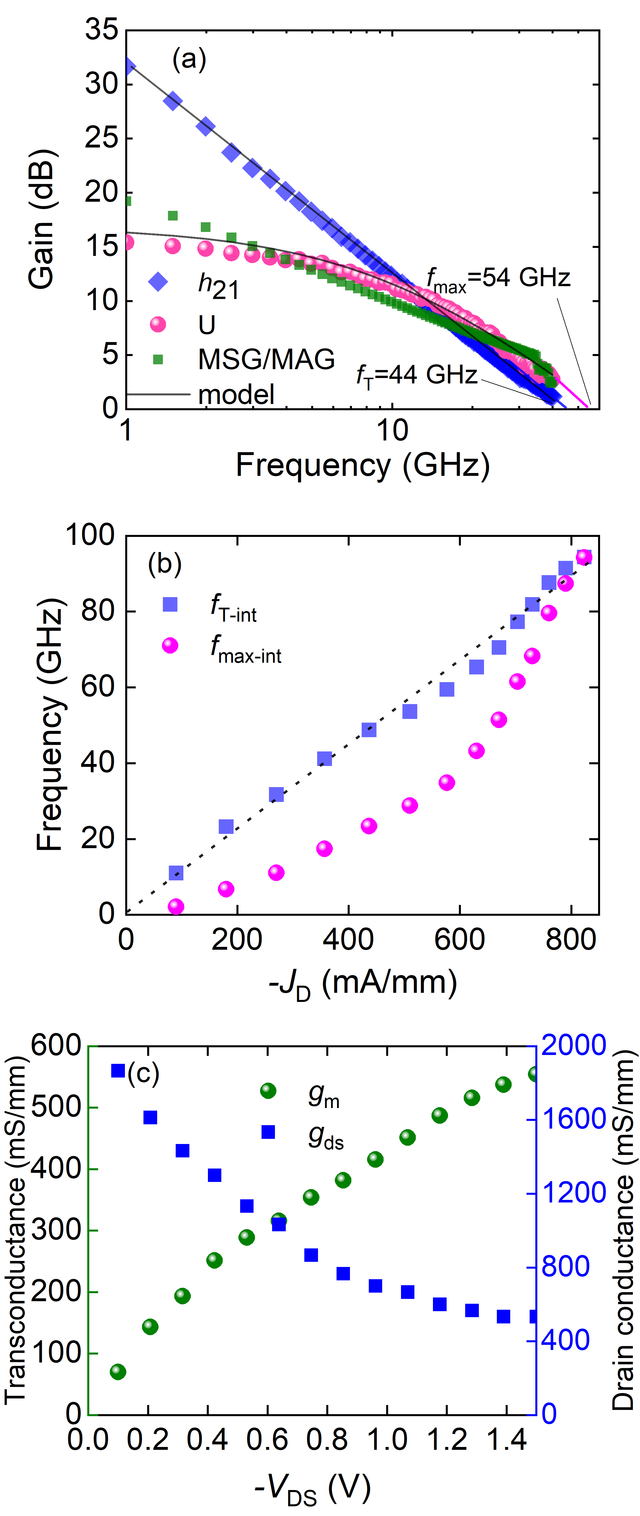
Fig. 2 shows the GFET transfer and output characteristics indicating typical GFET behavior. The vs. curve obtained for =1 V shows the conditions under which the high-frequency performance was measured. Fig. 3 summarizes the measurement results obtained for the same GFET biased for maximum gain. First, the frequency-dependent current gain (), the Mason’s unilateral power gain (), and the maximum stable gain/maximum available gain (MSG/MAG) obtained from the -parameters are shown in Fig. 3(a). An extrinsic as high as 44 GHz and an extrinsic as high as 54 GHz are indicated by the figure. To the best of our knowledge, this is the highest reported extrinsic performance of top-gated CVD GFETs so far [10, 11, 12, 13, 6, 7]. Fig. 3(b) shows an almost linear relationship between the intrinsic transit frequency and the drain current density , indicating a practically constant charge-carrier density throughout the whole drain bias range (0 to 1.5 V). This conclusion is based on the simple first-order assumption of an intrinsic transit frequency = and a drain current density =, where is the drift velocity, and is the elementary charge. Based on these assumptions an effective charge carrier concentration = 1.8 was obtained. Furthermore, the assumption of a constant charge-carrier density leads to the conclusion that the charge-carrier drift velocity profile can be obtained not only from the vs. (as in previous work [7]) but also directly from the output characteristic vs. . Finally, we can conclude that the effect of self-heating, typically resulting in an increasing charge-carrier density, is sufficiently low due to the high thermal conductivity of the diamond substrate.
From the broadband -parameter measurements, the bias-dependent small-signal equivalent circuit parameters , , , and were extracted and normalized by the gate width. The values of and are 50050 fF/mm, 45050 fF/mm, respectively, and are almost constant across the drain bias range. Figs. 3(c) shows conductances and versus the extrinsic drain voltage . The observed increase in transconductance and decrease in drain conductance with are the two main factors for the enhanced high-frequency performance of these devices. Other extrinsic circuit elements such as the pad inductance (= 13.8 pH, =1.6 pH, =5 pH), source/drain resistance (/=23 ), gate resistance, (=8 ), parasitic pad capacitances ( =15 fF, = 4 fF), and parasitic pad resistances (=21 k) are assumed to be bias-independent. Typically, due to zero-bandgap in monolayer graphene, GFETs reveal a linear output characteristic without drain current saturation resulting in a relatively high which has an adverse impact on the power gain i.e., limiting the . In this work, high current density due to high charge carrier velocity and significant drain current saturation due to velocity saturation are observed and verified by the drain current modeling. The drain current saturation results in low and, thus enhanced . Most promising way of increasing the high-frequency performance of GFET is by increasing the , which is proportional to the . The transconductance shown in Fig. 3(d) increases with the and shows signs of saturation at higher field.
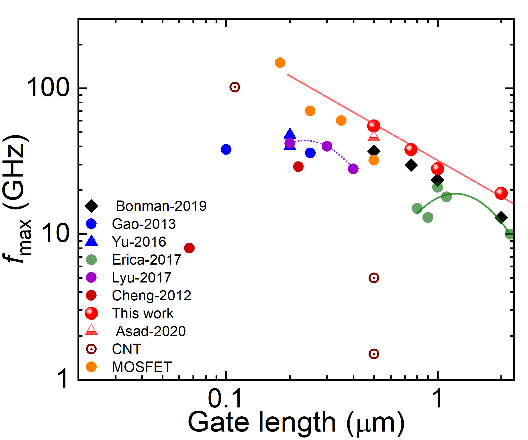
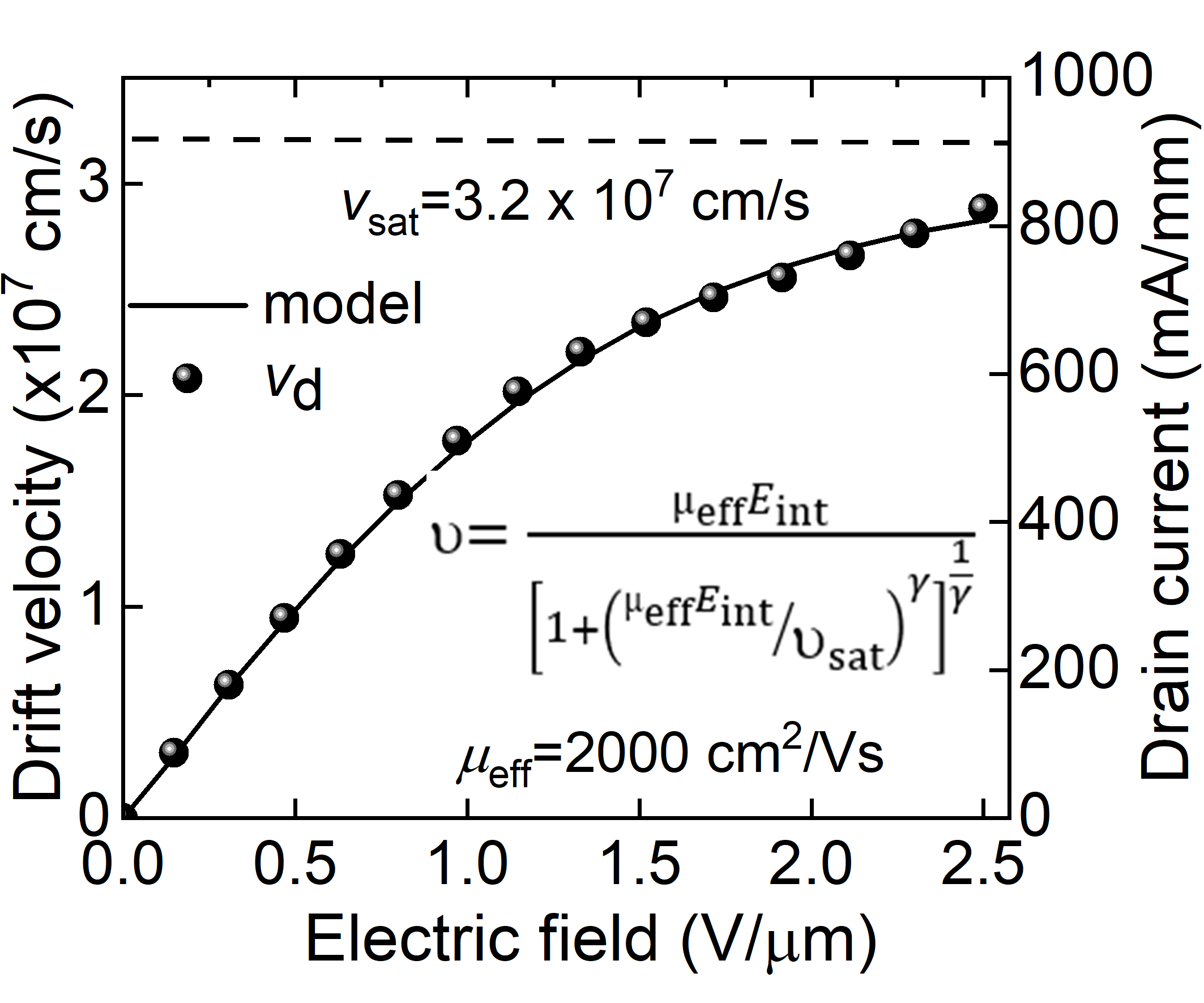
Fig. 4 shows the charge-carrier velocity found from the dependence of the drain current on the intrinsic drain field. The saturation velocity was derived by using the Caughey-Thomas velocity model [14] assuming a constant effective charge-carrier density – as previously concluded from the almost linear relationship between versus across the drain voltage range shown in Fig. 3(b). The in the diamond GFET is estimated being as high as 3.2 107 cm/s. For comparison, the in an hBN-encapsulated graphene Hall-bar test structure was reported to 5 107 cm/s [21].
To demonstrate the future prospects of the diamond GFET technology, the extrinsic performance of GFETs for different gate lengths is compared with published results in Fig. 5. In this work, the performance follows the solid trendline , typical for Si-MOSFET and HEMT technologies [4], which indicates a good scaling behaviour. For instance, we foresee that 100 GHz could be achieved for 200-nm GFET devices. The main improvements in the high-frequency performance and in the scaling behavior of the extrinsic are mainly attributed to a higher carrier velocity, improved current saturation, and reduced effects of self-heating.
4 Conclusions
In summary, the potential of top-gated graphene field-effect transistors on diamond substrate has been demonstrated. Substantial improvements in scaling behaviour and in maximum frequency of oscillation have been achieved due to the unique properties of diamond such as high surface-optical-phonon energy and high thermal conductivity when being used as a substrate. To reach the full potential of GFETs on diamond, both material quality and fabrication processes must be improved to achieve higher charge-carrier mobilities and saturation velocities.
References
- [1] K. S. Novoselov, A. K. Geim, S. V. Morozov, D. Jiang, Y. Zhang, S. V. Dubonos, I. V. Grigorieva, and A. A. Firsov, “Electric field effect in atomically thin carbon films,” Science, vol. 306, no. 5696, pp. 666–669, 2004, doi:10.1126/science.1102896.
- [2] M. C. Lemme, T. J. Echtermeyer, M. Baus, and H. Kurz, “A graphene field-effect device,” IEEE Electron Device Lett., vol. 28, no. 4, pp. 282–284, 2007, doi:10.1109/LED.2007.891668.
- [3] R. Cheng, J. Bai, L. Liao, H. Zhou, Y. Chen, L. Liu, Y.-C. Lin, S. Jiang, Y. Huang, and X. Duan, “High-frequency self-aligned graphene transistors with transferred gate stacks,” Proc. Natl. Acad. Sci., vol. 109, no. 29, pp. 11 588–11 592, 2012, doi:10.1073/pnas.1205696109.
- [4] F. Schwierz, “Graphene transistors: status, prospects, and problems,” Proc. IEEE, vol. 101, no. 7, pp. 1567–1584, 2013, doi:10.1109/JPROC.2013.2257633.
- [5] C. Yu, Z. He, Q. Liu, X. Song, P. Xu, T. Han, J. Li, Z. Feng, and S. Cai, “Graphene amplifier MMIC on SiC substrate,” IEEE Electron Device Lett., vol. 37, no. 5, pp. 684–687, 2016, doi:10.1109/LED.2016.2544938.
- [6] M. Bonmann, M. Asad, X. Yang, A. Generalov, A. Vorobiev, L. Banszerus, C. Stampfer, M. Otto, D. Neumaier, and J. Stake, “Graphene Field-Effect Transistors With High Extrinsic and ,” IEEE Electron Device Lett., vol. 40, no. 1, pp. 131–134, 2018, doi:10.1109/LED.2018.2884054.
- [7] M. Asad, K. O. Jeppson, A. Vorobiev, M. Bonmann, and J. Stake, “Enhanced high-frequency performance of top-gated graphene fets due to substrate- induced improvements in charge carrier saturation velocity,” IEEE Trans. Electron Devices, vol. 68, no. 2, pp. 899–902, 2021, doi:10.1109/TED.2020.3046172.
- [8] J. Isberg, J. Hammersberg, E. Johansson, T. Wikström, D. J. Twitchen, A. J. Whitehead, S. E. Coe, and G. A. Scarsbrook, “High carrier mobility in single-crystal plasma-deposited diamond,” Science, vol. 297, no. 5587, pp. 1670–1672, 2002, doi:10.1126/science.1074374.
- [9] G. Dambrine, A. Cappy, F. Heliodore, and E. Playez, “A new method for determining the fet small-signal equivalent circuit,” IEEE Trans. Microw. Theory Tech., vol. 36, no. 7, pp. 1151–1159, 1988, doi:10.1109/22.3650.
- [10] Z. Guo, R. Dong, P. S. Chakraborty, N. Lourenco, J. Palmer, Y. Hu, M. Ruan, J. Hankinson, J. Kunc, J. D. Cressler et al., “Record maximum oscillation frequency in c-face epitaxial graphene transistors,” Nano Lett., vol. 13, no. 3, pp. 942–947, 2013, doi:10.1021/nl303587r.
- [11] Y.-M. Lin, C. Dimitrakopoulos, K. A. Jenkins, D. B. Farmer, H.-Y. Chiu, A. Grill, and P. Avouris, “100-ghz transistors from wafer-scale epitaxial graphene,” Science, vol. 327, no. 5966, pp. 662–662, 2010, doi:10.1126/science.1184289.
- [12] Y. Wu, K. A. Jenkins, A. Valdes-Garcia, D. B. Farmer, Y. Zhu, A. A. Bol, C. Dimitrakopoulos, W. Zhu, F. Xia, P. Avouris et al., “State-of-the-art graphene high-frequency electronics,” Nano Lett., vol. 12, no. 6, pp. 3062–3067, 2012, doi:10.1021/nl300904k.
- [13] H. Lyu, Q. Lu, J. Liu, X. Wu, J. Zhang, J. Li, J. Niu, Z. Yu, H. Wu, and H. Qian, “Deep-submicron Graphene Field-Effect Transistors with state-of-art ,” Sci. Rep., vol. 6, p. 35717, 2016, doi:10.1038/srep35717.
- [14] D. Caughey and R. Thomas, “Carrier mobilities in silicon empirically related to doping and field,” Proc. IEEE, vol. 55, no. 12, pp. 2192–2193, 1967, doi:10.1109/PROC.1967.6123.
- [15] E. Guerriero, P. Pedrinazzi, A. Mansouri, O. Habibpour, M. Winters, N. Rorsman, A. Behnam, E. A. Carrion, A. Pesquera, A. Centeno et al., “High-gain graphene transistors with a thin top-gate oxide,” Sci. Rep., vol. 7, no. 1, pp. 1–7, 2017, doi:10.1038/s41598-017-02541-2.
- [16] Z. Wang, S. Liang, Z. Zhang, H. Liu, H. Zhong, L.-H. Ye, S. Wang, W. Zhou, J. Liu, Y. Chen et al., “Scalable fabrication of ambipolar transistors and radio-frequency circuits using aligned carbon nanotube arrays,” Adv. Mater., vol. 26, no. 4, pp. 645–652, 2014, doi:10.1002/adma.201302793.
- [17] C. Rutherglen, A. A. Kane, P. F. Marsh, T. A. Cain, B. I. Hassan, M. R. AlShareef, C. Zhou, and K. Galatsis, “Wafer-scalable, aligned carbon nanotube transistors operating at frequencies of over 100 ghz,” Nat. Electron, vol. 2, no. 11, pp. 530–539, 2019, doi:10.1038/s41928-019-0326-y.
- [18] P. De la Houssaye, C. Chang, B. Offord, G. Imthurn, R. Johnson, P. Asbeck, G. Garcia, and I. Lagnado, “Microwave performance of optically fabricated T-gate thin film silicon-on-sapphire based MOSFET’s,” IEEE Electron Device Lett., vol. 16, no. 6, pp. 289–292, 1995, doi:10.1109/55.790738.
- [19] L. Tiemeijer, H. Boots, R. Havens, A. Scholten, P. De Vreede, P. Woerlee, A. Heringa, and D. Klaassen, “A record high 150 GHz realized at 0.18 m gate length in an industrial RF-CMOS technology,” in International Electron Devices Meeting. Technical Digest (Cat. No. 01CH37224). IEEE, 2001, pp. 10–4, doi:10.1109/IEDM.2001.979471.
- [20] R. A. Johnson, P. R. de la Houssaye, C. E. Chang, Pin-Fan Chen, M. E. Wood, G. A. Garcia, I. Lagnado, and P. M. Asbeck, “Advanced thin-film silicon-on-sapphire technology: microwave circuit applications,” IEEE Trans. Electron Devices, vol. 45, no. 5, pp. 1047–1054, 1998, doi:10.1109/16.669525.
- [21] M. A. Yamoah, W. Yang, E. Pop, and D. Goldhaber-Gordon, “High-velocity saturation in graphene encapsulated by hexagonal boron nitride,” ACS nano, vol. 11, no. 10, pp. 9914–9919, 2017, doi:10.1021/acsnano.7b03878.