Role of surface termination in the metal-insulator transition of V2O3(0001) ultrathin films
Abstract
Surface termination is known to play an important role in determining the physical properties of materials. It is crucial to know how surface termination affects the metal-insulator transition (MIT) of V2O3 films for both fundamental understanding and its applications. By changing growth parameters, we achieved a variety of surface terminations in V2O3 films that are characterized by low energy electron diffraction (LEED) and photoemission spectroscopy techniques. Depending upon the terminations, our results show MIT can be partially or fully suppressed near the surface region due to the different filling of the electrons at the surface and sub-surface layers and change of screening length compared to the bulk. Across MIT, a strong redistribution of spectral weight and its transfer from high-to-low binding energy regime is observed in a wide-energy-scale. Our results show total spectral weight in the low-energy regime is not conserved across MIT, indicating a breakdown of ‘sum rules of spectral weight’, a signature of a strongly correlated system. Such change in spectral weight is possibly linked to the change in hybridization, lattice volume (i.e., effective carrier density), and spin degree of freedom in the system that happens across MIT. We find that MIT in this system is strongly correlation-driven where the electron-electron interactions play a pivotal role. Moreover, our results provide a better insight in understanding the electronic structure of strongly correlated systems and highlight the importance of accounting surface effects during interpretation of the physical property data mainly using surface sensitive probes, such as surface resistivity.
I Introduction
Study of the metal-insulator transition in strongly correlated transition metal oxides such as Ti2O3, VO2, V2O3, and NbO2 are still an active field of research for the understanding and tuning of MIT for their potential applications in intelligent windows and field-effect transistors Zhou et al. (2013); Yamamoto et al. (2019); Brockman et al. (2011). These materials are known to undergo a temperature-dependent MIT in concurrence with a structural transition Mott and Friedman (1974); Joshi et al. (2019). In addition to the structural transition, the magnetic transition also occur simultaneously in V2O3 and is found to play an important role in MIT Trastoy et al. (2018a). Numerous studies show, a small change of the crystal structure, by Cr or Ti substitution Kuwamoto et al. (1980); McWhan et al. (1969); Shin et al. (1995); Lupi et al. (2010) or applying pressure Limelette et al. (2003) can have a major effect on the MIT of bulk V2O3. Other factors such as surface reconstruction and lattice defects can also affect the MIT of these materials Wickramaratne et al. (2019); Panaccione et al. (2007). The breakdown of Mott physics at the surface of VO2 thin films is reported by Wahila et al. Wahila et al. (2020) due to the surface reconstructions/terminations. For V2O3 thin-films, various types of surface termination have been reported by several groups Dupuis et al. (2003); Pfuner et al. (2005); Feiten et al. (2015a) which can make the understanding of the physics of MIT even more complicated.
At room temperature, V2O3 is a paramagnetic metal (PM) with a corundum structure while at low temperature, below about 150-160 K, it undergoes a transition to an antiferromagnetic insulating (AFI) phase accompanied by a structural change from the trigonal (corundum) to a monoclinic one with a 1.4% volume increase. Despite the extensive studies of MIT on V2O3 single crystal and polycrystalline powder, contradictory results persist in thin-films Luo et al. (2004); Dillemans et al. (2014); Grygiel et al. (2007). Recently, Luo et al. Luo et al. (2004) have reported a thickness-dependent metal-insulator transition of V2O3 thin-film grown on Al2O3(0001) substrate. They argue that the MIT with decreasing film thickness is due to the increase of the lattice parameter ratio because of the substrate-induced strain in the films. Their results show the thicker films (20 nm) remain in the metallic phase down to 4 K. In contrast, Dillemans et al. Dillemans et al. (2014) have shown, all their films with thickness ranging from 473 nm grown on the same substrate (Al2O3) undergo temperature-dependent MIT. Further, x-ray diffraction (XRD) studies in these films (thickness range of 10-100 nm) do not show any systematic change of lattice parameters Grygiel et al. (2007). Schuler et al. Schuler et al. (1997) have addressed an impact of the synthesis conditions on MIT and growth modes of the films. All these together suggest the absence of MIT observed in ref. Luo et al. (2004); Grygiel et al. (2007) can not be explained only by considering c/a ratio change.
It is known that V2O3(0001) films generally contains various types of surface termination which changes upon growth conditions Feiten et al. (2015b, a); Dupuis et al. (2003); Pfuner et al. (2005). Films grown at ultra-high vacuum (UHV) in optimal growth condition favours the formation of vanadyl (V=O) terminated surface Feiten et al. (2015b, a). Further, annealing the V=O terminated films at higher oxygen partial pressure gives rise to a surface due to the removal of 1/3 or 2/3 of the V=O groups from the surface layer Dupuis et al. (2003); Pfuner et al. (2005). From the theoretical phase diagram Feiten et al. (2015b) of oxygen chemical potential vs. growth temperature, complete removal of V=O groups is also possible at even higher oxygen partial pressure and temperature which should reflect as a reconstructed O3 terminated (rec-O3) surface layer Feiten et al. (2015b); Kresse et al. (2004). The structural model for all these surface termination as obtained from density function theory (DFT) Feiten et al. (2015b) are shown in figure 1(e). Depending upon the terminations, the electronic structure at the surface/sub-surface is expected to deviate from its bulk and its impact should reflect on the electronic properties and MIT. Pfuner et al. Pfuner et al. (2005) have reported suppression of MIT for the terminated V2O3(0001) surface. It appears that during the interpretation of the experimental data such as surface resistivity, an account of the surface termination effect, in addition to the substrate-induced strain, is essential to get the complete picture of MIT. However, it is not typically discussed how breaking crystal symmetry via surface termination affects the MIT and detailed systematic spectroscopic studies are barely available in the literature. In general, in strongly correlated systems, the change of hybridization, lattice volume (electron density), spin degree of freedom can show unusual spectral evolution mainly in the low-energy scale Meinders et al. (1993); Kohno (2019); Rozenberg et al. (1996), however, there is still little understanding how MIT in V2O3 alters the low-energy physics.
Here, we study the effect of surface termination on the electronic structure of V2O3 films and its impact on MIT. To achieve this goal, well ordered V2O3(0001) surface has been grown on Ag(111) substrate with different oxygen partial pressures and substrate temperatures, following post-growth procedures. Our results show, at optimal growth condition, the V2O3(0001) surface is terminated by the V=O groups while annealing the film at higher oxygen partial pressure and temperature results in the surface structure due to the removal of V=O groups. Films directly grown at higher oxygen partial pressures and temperatures results in a nearly rec-O3-like surface. Partial to full suppression of MIT is observed by going from V=O to and rec-O3-like surfaces. We also show that MIT in this system is strongly correlation driven and it is associated with a strong redistribution of orbital occupancy in the much wider energy scale than previously thought. Further, we discuss the possible origin of unusual spectral weight enhancement in the low-energy-scale that occurs when the system is cooled below MIT.
II Results and discussion
II.1 Surface structure of V2O3 films
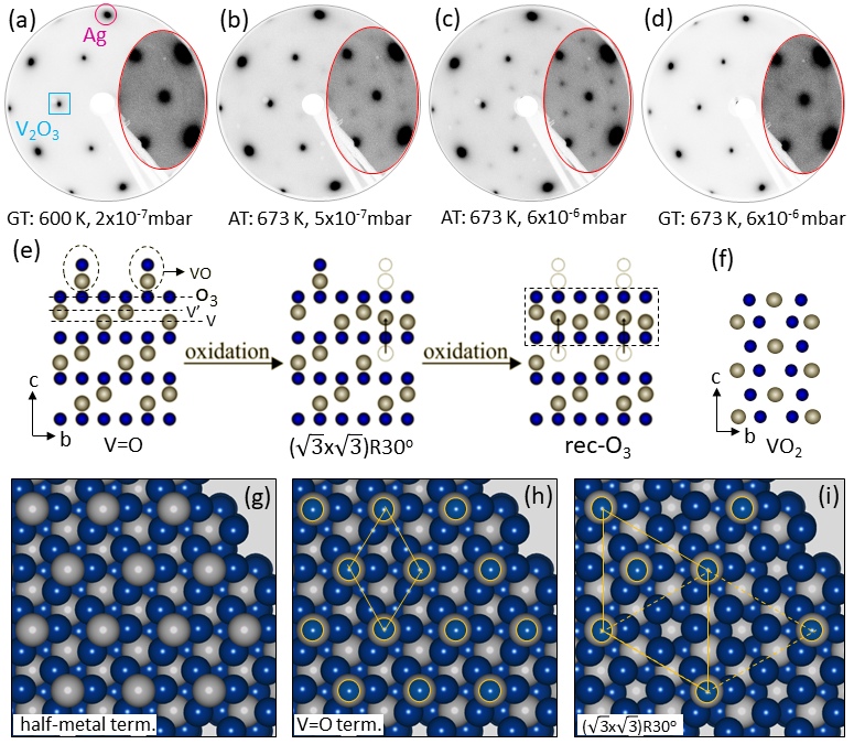
Figure 1(a) shows the LEED image of 30 MLE V2O3 films on Ag(111), grown at a substrate temperature of 600 K in presence of = 210-7 mbar followed by UHV annealing at 773 K. The position of the first order diffraction spots from Ag(111) (before deposition of films) and V2O3 are marked. LEED pattern shows structure w.r.t Ag(111) substrate. It is expected as the lattice parameter of the V2O3(0001) surface (4.95 Å) is very close to the times of Ag(111) lattice parameter (2.89=5.0 Å) with only 1% lattice mismatch, favouring the growth of epitaxial V2O3(0001) films. This structure can be thought as (11) structure w.r.t the V2O3(0001) basis vectors. Throughout the paper, we will call this structure as (11) structure for the simplicity of our discussions. The (11) structure have been also observed by previous studies of V2O3 films on Au(111) and W(110) substrate at similar growth conditions which was regarded as a V=O terminated V2O3(0001) surface Dupuis et al. (2003); Pfuner et al. (2005). The V=O terminated surface may be thought as an ideal half-metal terminated surface (figure 1(g)) of V2O3(0001) with one additional oxygen atom bonded on top of each outermost V atom (figure 1(h)). Annealing the V=O terminated surface in presence of oxygen shows additional spots (superstructures) that form structure w.r.t. (11)-V2O3 as shown in figure 1(b). These superstructure spots gain intensities upon further annealing the sample at higher oxygen pressure as can be seen in figure 1(c). The structure could originate by removing the 1/3 or 2/3 amount of V=O groups from the V=O terminated surface Schoiswohl et al. (2004); Feiten et al. (2015a). The surface atomic configuration is shown in figure 1(i), where the rhombus with solid and dotted lines represent the surface unit cell corresponding to the removal of 1/3 and 2/3 of V=O groups, respectively. Relatively lower intense and broad superstructure spots in figure 1(b) compare to figure 1(c) may indicate that the removal of V=O groups is less uniform and lower in numbers in figure 1(b) than in figure 1(c). Similar behavior has been reported by Schoiswohl et al. Schoiswohl et al. (2004) using combined scanning tunneling microscopy (STM) and LEED study.
Figure 1(d) shows the LEED pattern of films that has been directly grown at higher temperature and oxygen partial pressure (673 K, = 610-6 mbar). The LEED pattern shows mainly (11) structure but additional broad spots with extremely faint intensities can be visible at higher brightness/contrast (inside oval) that form structure. Feiten et al. Feiten et al. (2015b), have pointed out that both V=O and rec-O3 terminated surface exhibit identical reflex patterns and indicated that the LEED-IV measurements might be helpful to distinguish them. Further, DFT calculation Feiten et al. (2015b) also predicts that the rec-O3 surface termination favors at higher temperature and oxygen partial pressure (see the structural model in figure 1(e)). Thus, the presence of extremely low intense structure could mean that only locally 1/3 or 2/3 amount of V=O groups are missing or left. In other words, this surface is either very close to the V=O terminated or rec-O3 terminated surface.
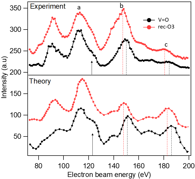
To get more insight into the surface structure, we have performed experimental LEED-IV measurements and compared them with the reported theoretical results Feiten et al. (2015b). The top panel in figure 2 shows the experimental LEED-IV curves extracted from the first-order diffraction spots of V2O3 corresponding to the figure 1(a) (black) and figure 1(d) (red), respectively. The bottom panel in figure 2 shows the simulated LEED-IV curves for the V=O and rec-O3 terminated surfaces Feiten et al. (2015b). Between the two experimental curves, there are some significant differences can be observed such as black spectra shows prominent two peak structure for the peak ‘a’, while peaks ‘b’ and ‘c’ shifted towards the higher energy compared to the red spectra. By comparing with the theoretical spectra, it appears that the position of peaks in black experimental spectra better match with the V=O terminated while the red spectra with the rec-O3 terminated surface. Although it is not perfectly rec-O3 terminated surface as in that case it would show perfectly () LEED pattern Feiten et al. (2015b), but we will call it rec-O3-like due to its similarities with the LEED-IV curves with the rec-O3 terminated surface. We note that the position of peaks in the experimental I-V curves are in agreement with the theoretical curves whereas peak intensities differ. The experimental curves are not normalized by the incident electron beam-current that could produce the observed intensity differences. Unfortunately, we could not correct it as there were some technical issues with the beam-current reader during I-V data acquisition. The normalization can only change the intensity of the peaks, not the peak features or their position. Thus, it will not affect the main claims of our study.
II.2 Electronic structure and MIT of V2O3 films
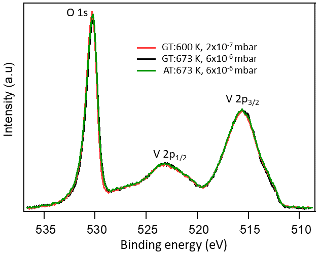
Understanding the chemical composition of these films is essential as vanadium may exist at different oxidation states (V+2 to V+5 ) depending upon the growth conditions. The most common way to directly access the chemical state of materials is to perform the XPS measurements. Figure 3 shows the O , V 2p1/2 and V 2p3/2 core-levels of V=O, , and rec-O3 terminated films. Despite the different surface structures observed in LEED, all the XPS spectra show very similar spectral features, indicating that they have a similar chemical composition in the bulk. We note that depending upon the used photon energy, XPS can be surface or bulk sensitive as its probing depth varies depending upon materials, the kinetic energy, and photoemission angle of the photoelectrons being measured Brundle and Crist (2020). Here, the kinetic energy of the V 2p photoelectrons measured using Al Kα (hv=1486.6 eV) is 965 eV that corresponds to 2.06 nm and probing depth 3 6.2 nm. Where is the attenuation length (mean free path) of photoelectrons. As the probing depth, 6.2 nm is comparable to the film thickness 6.57 nm, thus the surface effect is expected to be suppressed here.
XPS spectra were fitted (not shown) to extract the exact peak position and their full width at half maximum (FWHM). The details of fitting can be found elsewhere in our previous study Kundu and Menon (2017). The obtained peak position of O , V 2p1/2 and V 2p3/2 core-levels are 530.2 eV, 522.85 eV and 515.6 eV, respectively. In the case of vanadium oxide, the most common way to identify the exact phase is to measure the energy separation () between the O and V 2p3/2 core-levels and their FWHM Mendialdua et al. (1995). Here, the obtained value of is 14.7 eV and FWHM of O and V 2p3/2 peaks are 1.3 eV and 4.05 eV, respectively. All these values lie in the stoichiometric region of V2O3 Kundu and Menon (2017); Sawatzky and Post (1979). The overall spectral line-shape is also in good agreement with the V2O3 films Kundu and Menon (2017); Sawatzky and Post (1979); Kamakura et al. (2004). These results are in contrast with the DFT predictions Feiten et al. (2015b), as the bulk phase of rec-O3 terminated films is expected to be already in the region of V2O5 stoichiometry. This inconsistency may come from the overestimation of the Coulomb correlation effects in DFT calculation and the choice of exchange-correlation functional. In our experimental growth conditions, it may be possible that the formation of a higher oxidation state in bulk is just prevented by kinetic limitations.
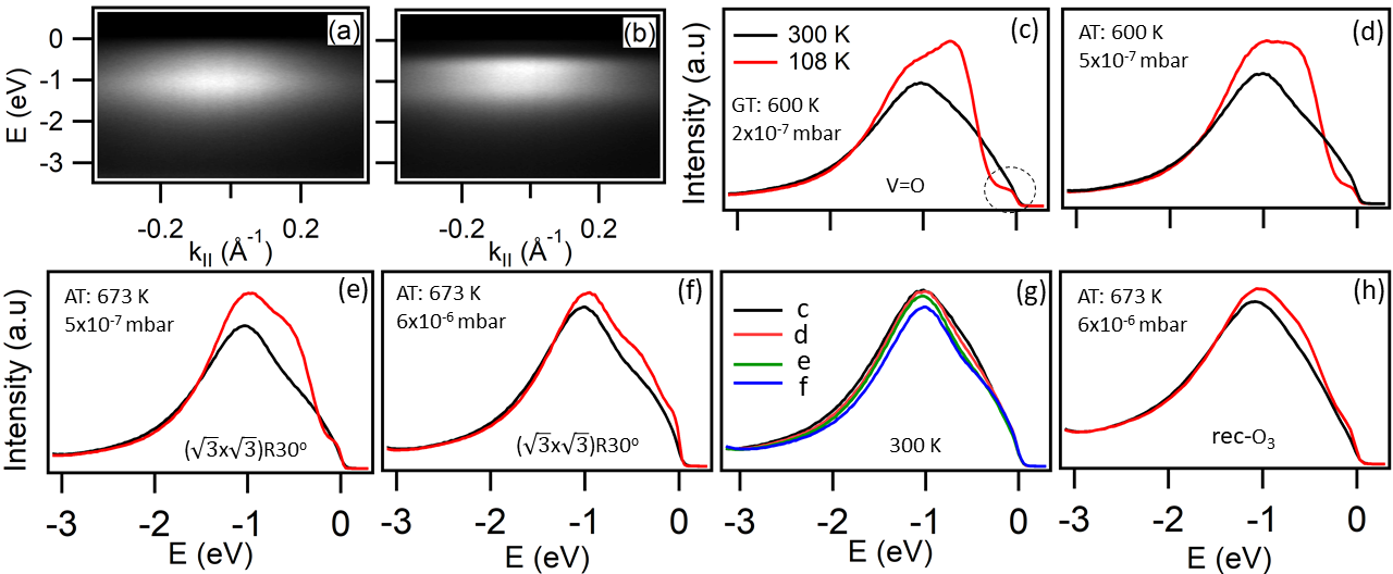
Further, it is important to know how surface termination affects the electronic structure and the MIT. Figure 4(a) and (b) show the ARPES intensity plots within the V region of V=O terminated V2O3 films, above and below MIT temperatures, respectively. The energy distribution curves (EDCs) obtained from figure 4(a) and (b) are shown in figure 4(c). In pure V2O3, V3+ has two electrons, occupying the triply degenerate (a1g, e) orbitals, split into a lower e doublet and an upper singlet in the trigonal crystal field (CF) of PM phase. In the low-temperature monoclinic phase, the additional low-symmetry CF component lifts e degeneracy. Moreover, EDCs of V region is dominated by e and a1g orbital. In the paramagnetic phase (figure 4(a)), the bands at -1.1 eV and -0.4 eV are arises from the lower Hubbard band (LHB) and quasiparticle peak (QP), respectively, according to the previous studies Mo et al. (2003); Rodolakis et al. (2009). The QP is broad and less intense due to the lower photon energy (21.2 eV) used in our experiment, where we are extremely sensitive to the surface. Previous studies also show less intense QP at the surface than bulk due to the enhanced correlation at the surface region relative to the bulk Mo et al. (2003). This is also in line with the DFT+ dynamical mean-field theory (DMFT) results, where it has been shown that a dead layer forms below the surface of V2O3, where quasiparticles are exponentially suppressed Borghi et al. (2009).
In figure 4(c), a significant change in spectral weight near Fermi level (EF) and its shifts towards the higher binding energy is observed when the sample is cooled below the MIT temperature. The observed behavior is mainly caused by the change in orbital occupancy in a1g and e orbital of V 3d across MIT, as observed in x-ray absorption spectroscopy (XAS) measurements Park et al. (2000). By lowering the temperature from 300 K (PM) to 108 K (AFI), it seems like the spectral weight is transferred from QP to the LHB side and the QP and LHB are shifted by 200 meV and 80 meV, respectively, towards higher binding energy. Total width (FWHM) of the V region (and LHB) also changes from 1.85 eV (1.4 eV) to 1.54 eV (1.24 eV) by going from PM to AFI phase. These values are obtained from fitting the spectra (see supplementary material, figure S1). According to the Hubbard model, decrease of LHB width () and its shift towards the higher binding energy, implies that the on-site Coulomb interactions (), as well as correlation () of the system, gets enhanced in the AFI phase compared to the PM phase. This suggests, MIT in V2O3 is strongly correlation driven, where the electron-electron correlation plays an important role. Although the Hubbard model ignores the degeneracy of bands, which is crucial for understanding the magnetic structures Castellani et al. (1978), it seems well captures the interplay between the electron-electron interactions and kinetic energy. The change of and across the phase transition are most likely due to a change of lattice parameter (change the hopping parameters) and effective screening length. Additionally, in the AFI phase, the scattering rate is also found to decrease which might sharpen the bandwidth as well Deng et al. (2014). From PM to AFI transition, an increase of and decrease of values are also reported by Rozenberg et al. Rozenberg et al. (1995) using optical measurements, similar to our observation.
However, it is not clear whether the QP band is totally absent in the AFM phase or it just shifts towards the higher energy with a redistribution of spectral weight. Across MIT, similar spectral features like our results were also reported for the V=O terminated V2O3 films Pfuner et al. (2005) and bulk single crystals Mo et al. (2006). This apparent shift of the PM phase spectrum across the MIT has been also found in a recent full-orbital DMFT calculation Anisimov et al. (2005), although the actual shape and peak position of the theoretical spectrum has different from the experimental spectra. Other DFT+DMFT calculations Lechermann et al. (2018); Leonov et al. (2015) incorporating full charge self-consistency were unable to capture the complex ‘two-peak structure of the LHB in the insulating (AFI) phase. We note that all these calculations were performed without accounting the exact spin-structure of the AFI phase of V2O3 and some of them only account the PM crystal structure, which may produce the observed discrepancy between theory and experiment. Trastoy et al. have also shown the importance of magnetic structure in MIT of V2O3 using resistivity and magnetoresistance measurements, combined with the theoretical calculations Trastoy et al. (2018a).
Besides, in figure 4(c), we observe a small Fermi-edge-like feature (enclosed by a dotted circle) at EF in the 108 K spectra which hinders the opening of a full energy gap at EF. This feature is not resolved in the 300 K spectra as it masks by the QP peak. By comparing with the theoretical layer-resolved density of state calculation Kresse et al. (2004), it appears that this edge-like feature is most probably originating from the V=O groups at the surface of the film. The theoretical data clearly shows the presence of a small density of states (DOS) at EF, which arises from a VO-like surface layer. This feature gains its intensity when measurements were performed using He IIα than He Iα (see supplementary information, figure S2) that strongly suggest its surface-related origin, as He IIα is more surface sensitive than He Iα. Furthermore, as VO does not show temperature-dependent MIT thus, the DOS originating from VO should remain at the same energy position both below and above MIT temperatures, which agrees with our results. This peak (V=O related) forms a Fermi-edge-like feature as it is cut by the Fermi Dirac distribution function at EF. We also vary the substrate temperature, a different substrate such as W(110), and oxygen partial pressure in a wide range but this feature was always present with a slight variation of intensity, depending upon the growth condition. According to Schoiswohl et al. Schoiswohl et al. (2004), V2O3 films grown at optimal condition followed by UHV annealing produce large-area films with fully covered V=O groups at the surface. In agreement, upon post-annealing the film in UHV, we also observe the intensity of the Fermi-edge-like feature and other V=O-related peaks are enhanced (see supplementary information figure S3). Possibilities of Ag segregation from substrate or formation of microcracks in the film can be ruled out, as no intensity enhancement of Ag-related peaks is observed (figure S3). Our previous study shows strong enhancement of Ag-related peak intensity when Ag segregates on V islands Kundu and Menon (2018). However, our study can not completely rule out the possibility of the presence of some precursor metallic phase even at 108 K, as the coexistence of microscopic metallic and insulating islands was found in a wide temperature range for Cr-doped V2O3 sample Lupi et al. (2010). Moreover, It is very unlikely that the V=O surface layer with its different geometry and electronic structure can support the MIT. Thus, the observation of spectral change across MIT in figure 4(c) and opening of a partial energy gap below MIT temperature, clearly suggest that the MIT in the bulk of the V2O3 film is communicated through the V=O surface layer.
Post annealing the V=O terminated films with increasing oxygen partial pressure and temperature are shown in figure 4(d)-(f). It can be seen that MIT is progressively weakened and completely suppressed by going from figure 4(d) to figure 4(f). The complete suppression of MIT is also observed for the rec-O3 like surface as shown in figure 4(h). In figure 4(e), change of spectral weight across MIT is still observed but without a gap at EF, whereas in figure 4(f), the spectral change is minimal and MIT is completely suppressed. In figure 4(g), all the EDCs from the figure 4(c) to (f) films taken at 300 K are plotted together. It is evident that with increasing oxygen partial pressure and temperatures, the total area of the V 3 region (03 eV) decreases about 16% (from figure 4(c) to (f)) which suggests a decrease of 3 electrons from 2 for V2O3 to the lower numbers, near the surface layer. The decrease in electron counts suggests that the surface is getting more oxygen-rich. A similar change of spectral features and decrease of V 3 area are reported for bulk V2-yO3 sample Kim et al. (1998). These suggest that the bulk MIT of V2O3 films are more effectively screen for the and rec-O3 like oxygen-rich surfaces than (11) V=O terminated surface. Suppression of MIT near the surface region can be understood by considering the structural change which occurs during the formation of rec-O3 and surfaces, where the removal of each V=O group exposes three oxygen atoms of the underlying O3 plane (see the structural model in figure 1(g) and (i)). To maintain thermodynamical equilibrium, the surface region, including subsurface layers relaxes and undergoes rearrangements (figure 1(e)) Schoiswohl et al. (2004), which strongly deviates from corundum bulk structure, whereas for V=O surface, only the top layer gets affected while subsurface layers preserve their bulk structure. Suppression of MIT is also observed in resistivity measurements for the oxygen-rich sample Trastoy et al. (2018b). Surface termination act as a charge doping (here, hole doping) to the surface layers, thus drastically alter the MIT characteristics by pushing the -filling further or closer to the Mott criterion Lee et al. (2019).
We note that for rec-O3 and (underlying surface below the removed V=O groups) structures, the surface has a stacking sequence -V2O3-V-O3V3O3 which may be thought of as an O3V3O3 trilayer structure with a formal VO2 stoichiometry on top of the single V terminated bulk structure (see figure 1(e)). As VO2 is known to show MIT below 320 K Choi et al. (2021), both the 300 K and 108 K EDCs corresponding to these structures would show insulating behavior or at least the 108 K EDCs, as the underlying structure is still V2O3 which only shows MIT at low temperature. While our data show metallic behavior in both temperatures (figure 4(f) and (h)). This behavior suggests that the chemical composition alone cannot determine the MIT properties but a combination of chemical composition and crystal structure does. The structural difference between the trilayer stacking with VO2 composition and the bulk VO2 are shown in figure 1(e) and (f), respectively.
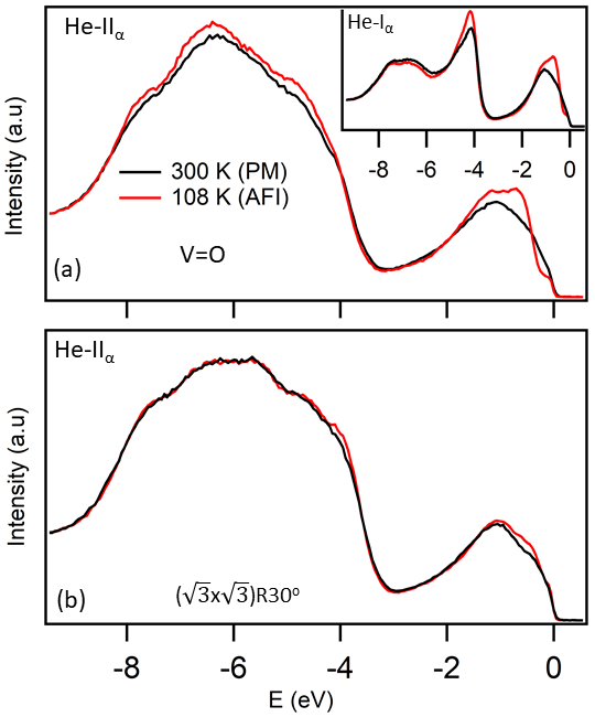
We also note that in figure 4(c), the integrated area within the energy ranges, 0 to -3.0 eV is enhanced by 16.5% in the AFI (108 K) phase compared to PM (300 K), indicating breakdown of ‘sum rules of spectral weight’ in that energy regime which in turn suggests the presence of strong correlation in the system Meinders et al. (1993); Kohno (2019). Theoretically, the breakdown of ‘sum rules of spectral weight’ in the low-energy scale has been found in strongly correlated systems when a change of hybridization and/or electron density are introduced in the system Meinders et al. (1993); Kohno (2019). A question may arise, what is the source of this extra spectral weight? To get further insight, we have plotted EDCs in a wide energy window as shown in figure 5(a). Not only in the lower energy regime, but a strong redistribution of spectral weight is also observed within the whole energy range, 0 to -9.5 eV. Spectra taken at He Iα photons (inset of figure 5(a)) also shows similar behavior. The main difference between He Iα and He IIα spectra is that spectral weight within the energy ranges, -5 to -8 eV decreases in the AFI phase for He Iα whereas increases for He IIα. The different behavior could be associated with the kz dependence of spectral weight transfer Kohno (2019). The estimated increase of spectral weight in the AFI phase within the whole measured energy ranges are 3.5% and 6% for He Iα and He IIα, respectively. Previous photoemission studies performed on the Cr-doped V2O3 sample, between the paramagnetic insulator (PI) and the crossover regime also found spectral weight redistribution within the whole valence band region Mo et al. (2004). In contrast, their results show that the V 3d and O 2p spectral weight conserved separately within these two regions (PI and crossover). Similar to our results, optics experiment also shows total spectral weight across MIT is not conserved within energy range, 0 to 6 eV above the Fermi energy Qazilbash et al. (2008); Stewart et al. (2012); Rozenberg et al. (1995). Interestingly, it can be seen that for the oxygen-rich surface, the spectral weight change is almost negligible as shown in figure 5(b). These results confirming that the spectral weight enhancement and its redistribution are strongly related to the MIT transition.
The change in lattice structure and volume that occurs across MIT may have important consequences in the observed spectral weight renormalization (redistribution), as it alters the hybridization strength between different orbital as well as carrier density (carriers/volume) that strongly affect the orbital occupancy. In general, electronic states (bands) are usually considered invariant regardless of the electron density in a band picture. However, in interacting systems, the spectral-weight distribution changes depending on the electron density, and electronic states can even emerge or disappear Kohno (2019); Meinders et al. (1993). Furthermore, Kohno et al., Kohno (2019), have explicitly shown that the electronic excitations much away from the Fermi level can also become dominant and exhibit significant characteristics due to the change in electron density. Keeping in mind that, as we are not externally doping carriers in the system then the total carriers should be conserved but carrier density may change across MIT due to the change in lattice volume. Thus, one feasible interpretation for an apparent increase of spectral weight within 0 to -9.5 eV regime would be that the transfer of spectral weight occurs from much deeper to the lower binding energy side, due to the redistribution of orbital occupancy in the larger energy regime. It can be clearly seen from the He Iα data (inset of figure 5) that the spectral weight decreased in the higher binding energy side whereas increased going towards the Fermi energy. Further, theoretical study considering the antiferromagnetic ordering in V2O3 also find evidence of spectral weight transfer from higher to lower binding energy side compared to the PM phase Rozenberg et al. (1996). All these together suggest that the strong change in spectral weight across MIT is due to the complex interplay between the charge, orbital and spin degree of freedom in this system.
We also note that MIT of V2O3(0001) films have been studied by several groups by resistivity measurement Luo et al. (2004); Dillemans et al. (2014); Grygiel et al. (2007); Brockman et al. (2011). Unlike bulk V2O3 single crystals, in most of the thin-films, resistivity vs. temperature curve do not show sharp transition Dillemans et al. (2014); Grygiel et al. (2007); Brockman et al. (2011) and in some cases, the system remains in the metallic phase Luo et al. (2004); Grygiel et al. (2007). Substrate-induced strain effect in the films has been considered as an origin of the absence of the temperature-driven MIT Luo et al. (2004); Grygiel et al. (2007). In contrast, Dillemans et al. Dillemans et al. (2014) have shown that V2O3(0001) films grown on the same substrate (Al2O3) undergo temperature-dependent MIT, questions the validity of strain-induced loss of MIT in this system. Our results highlight, in addition to the epitaxial strain, there should be surface termination effects, and combining these two can better explain the observed resistivity change in a wide temperature scale or suppression/absence of MIT in most of the thin-film systems.
II.3 Conclusion
In summary, we have grown ultrathin films of V2O3(0001) with various surface terminations and characterized them using LEED and photoemission spectroscopy techniques. We have shown that depending on the types of termination, MIT at the surface region can be partially or fully suppressed. This suggests high sensitivity of the Mott metal-insulator transition to the local environment, consistent with recent theoretical predictions Lechermann et al. (2018). We have also shown, upon MIT, the spectral weight is not only shifted from QP to the LHB, but a huge redistribution of spectral weight is observed within the whole valence band. Total spectral weight was found to be not conserved within the energy ranges, 0 to -9.5 eV which indicates that the spectral weight is redistributed in much larger energy, suggesting the system is heavily correlated. Such enhancement of spectral weight in the low-energy regime is mainly due to the spectral weight transfer from higher to lower binding energy regime due to the change in complex interplay between the charge, orbital and spin degree of freedom in this system that occurs during MIT. We have also shown that in addition to the other effects, taking into account surface termination can better explain the anomaly observed in the resistivity data of V2O3. We expect that similar behavior would be at play for other complex oxides and the interpretation of physical properties data (mainly using surface sensitive probe) requires more attention. Furthermore, the observed complex structure of LHB in our experiment (in the AFI phase) is not reproduced by the currently available theories, including DFT+DMFT. Thus, we believe that our results might help in the further development of the theoretical understanding of MIT in strongly correlated systems.
III Experimental
The Ag(111) substrate was cleaned by repeated cycles of Ar+ ion sputtering (600 eV, 1 A) for 15 min followed by annealing at 823 K for 20 min until a sharp LEED pattern was observed. The substrate preparation, growth, and LEED measurements were performed in the preparation chamber with a base pressure of 110-10 mbar. Vanadium was evaporated from a well-degassed water-cooled e-beam evaporator at a constant rate of 0.3 Å/min in oxygen partial pressure range of P(O2)= -6 mbar for the deposition of the V2O3 film, while during deposition, the substrate temperature was varied between at 473673 K. The rate of V-deposition was calibrated with a water-cooled quartz crystal thickness monitor. One monolayer equivalent (MLE) of vanadium oxide film is defined as the atomic density corresponding to 1 ML vanadium on Ag(001), i.e, 1.751019 atoms/m2, under oxygen atmosphere. We have grown 30 MLE films that appear 6.57 nm as estimated from the attenuation of Ag 3d core-level intensity. To achieve a high-quality surface, the film was annealed at 673773 K for 10 min in UHV. The sample temperature was measured by a K-type thermocouple, in contact with the Ag crystal. The crystalline quality of the film and the symmetry directions were determined by a four-grid LEED apparatus while a highly-sensitive Peltier-cooled 12-bit CCD camera was used to collect the LEED images. Photoemission spectroscopic measurements, XPS, and ARPES were performed in an analysis chamber having a base pressure better than 810-11 mbar. ARPES experiments were performed using a combination of VG SCIENTA-R4000WAL electron energy analyzer with a 2D-CCD detector and a high flux GAMMADATA VUV He lamp attached to a VUV monochromator, which has been described in detail elsewhere Mahatha and Menon (2010). The ARPES measurements were performed using monochromatized ultraviolet He Iα(21.2 eV) and He IIα (40.8 eV) resonance lines, while the XPS measurements were performed with Al Kα monochromatic X-ray source (1486.6 eV) from VG SCIENTA. At room temperature (RT), the total experimental energy resolution was about 100 meV for the UPS (using He Iα and He IIα photons) while for the monochromatic XPS the energy resolution was set to about 600 meV.
IV acknowledgement
The Micro-Nano initiative program of the Department of Atomic Energy (DAE), Government of India, is acknowledged for generous funding and support for this work. During writing the paper, A.K.K receives funding from US Department of Energy, Office of Basic Energy Sciences, contract no. DE-SC0012704. The authors thank T. Valla, A. Samanta, and S. K. Mahatha for the helpful discussions.
References
- Zhou et al. (2013) J. Zhou, Y. Gao, Z. Zhang, H. Luo, C. Cao, Z. Chen, L. Dai, and X. Liu, Sci. Rep. 3, 3029 (2013).
- Yamamoto et al. (2019) M. Yamamoto, R. Nouchi, T. Kanki, A. N. Hattori, K. Watanabe, T. Taniguchi, K. Ueno, and H. Tanaka, ACS applied materials & interfaces 11, 3224 (2019).
- Brockman et al. (2011) J. Brockman, N. Aetukuri, T. Topuria, M. Samant, K. Roche, and S. Parkin, Applied Physics Letters 98, 152105 (2011).
- Mott and Friedman (1974) N. F. Mott and L. Friedman, Philosophical Magazine 30, 389 (1974).
- Joshi et al. (2019) T. Joshi, E. Cirino, S. A. Morley, and D. Lederman, Phys. Rev. Materials 3, 124602 (2019).
- Trastoy et al. (2018a) J. Trastoy, A. Camjayi, J. del Valle, Y. Kalcheim, J.-P. Crocombette, J. Villegas, M. Rozenberg, D. Ravelosona, and I. K. Schuller, arXiv preprint arXiv:1808.03528 (2018a).
- Kuwamoto et al. (1980) H. Kuwamoto, J. Honig, and J. Appel, Physical Review B 22, 2626 (1980).
- McWhan et al. (1969) D. McWhan, T. Rice, and J. Remeika, Physical Review Letters 23, 1384 (1969).
- Shin et al. (1995) S. Shin, Y. Tezuka, T. Kinoshita, T. Ishii, T. Kashiwakura, M. Takahashi, and Y. Suda, Journal of the Physical Society of Japan 64, 1230 (1995).
- Lupi et al. (2010) S. Lupi, L. Baldassarre, B. Mansart, A. Perucchi, A. Barinov, P. Dudin, E. Papalazarou, F. Rodolakis, J. P. Rueff, J. P. Itié, S. Ravy, D. Nicoletti, P. Postorino, P. Hansmann, N. Parragh, A. Toschi, T. Saha-Dasgupta, O. K. Andersen, G. Sangiovanni, K. Held, and M. Marsi, Nature communications 1, 1 (2010).
- Limelette et al. (2003) P. Limelette, A. Georges, D. Jérome, P. Wzietek, P. Metcalf, and J. Honig, Science 302, 89 (2003).
- Wickramaratne et al. (2019) D. Wickramaratne, N. Bernstein, and I. Mazin, Physical Review B 99, 214103 (2019).
- Panaccione et al. (2007) G. Panaccione, M. Sacchi, P. Torelli, F. Offi, G. Cautero, R. Sergo, A. Fondacaro, C. Henriquet, S. Huotari, G. Monaco, and L. Paolasini, Journal of Electron Spectroscopy and Related Phenomena 156, 64 (2007).
- Wahila et al. (2020) M. J. Wahila, N. F. Quackenbush, J. T. Sadowski, J.-O. Krisponeit, J. I. Flege, R. Tran, S. P. Ong, C. Schlueter, T.-L. Lee, M. E. Holtz, et al., arXiv preprint arXiv:2012.05306 (2020).
- Dupuis et al. (2003) A.-C. Dupuis, M. A. Haija, B. Richter, H. Kuhlenbeck, and H.-J. Freund, Surface science 539, 99 (2003).
- Pfuner et al. (2005) F. Pfuner, J. Schoiswohl, M. Sock, S. Surnev, M. Ramsey, and F. Netzer, Journal of Physics: Condensed Matter 17, 4035 (2005).
- Feiten et al. (2015a) F. E. Feiten, H. Kuhlenbeck, and H.-J. Freund, The Journal of Physical Chemistry C 119, 22961 (2015a).
- Luo et al. (2004) Q. Luo, Q. Guo, and E. Wang, Applied physics letters 84, 2337 (2004).
- Dillemans et al. (2014) L. Dillemans, T. Smets, R. Lieten, M. Menghini, C.-Y. Su, and J.-P. Locquet, Applied Physics Letters 104, 071902 (2014).
- Grygiel et al. (2007) C. Grygiel, C. Simon, B. Mercey, W. Prellier, R. Frésard, and P. Limelette, Applied Physics Letters 91, 262103 (2007).
- Schuler et al. (1997) H. Schuler, S. Klimm, G. Weissmann, C. Renner, and S. Horn, Thin Solid Films 299, 119 (1997).
- Feiten et al. (2015b) F. E. Feiten, J. Seifert, J. Paier, H. Kuhlenbeck, H. Winter, J. Sauer, and H.-J. Freund, Physical Review Letters 114, 216101 (2015b).
- Kresse et al. (2004) G. Kresse, S. Surnev, J. Schoiswohl, and F. Netzer, Surface science 555, 118 (2004).
- Meinders et al. (1993) M. Meinders, H. Eskes, and G. Sawatzky, Physical Review B 48, 3916 (1993).
- Kohno (2019) M. Kohno, Physical Review B 100, 235143 (2019).
- Rozenberg et al. (1996) M. Rozenberg, G. Kotliar, and H. Kajueter, Physical Review B 54, 8452 (1996).
- Schoiswohl et al. (2004) J. Schoiswohl, M. Sock, S. Surnev, M. Ramsey, F. Netzer, G. Kresse, and J. N. Andersen, Surface science 555, 101 (2004).
- Brundle and Crist (2020) C. R. Brundle and B. V. Crist, Journal of Vacuum Science & Technology A 38, 041001 (2020).
- Kundu and Menon (2017) A. K. Kundu and K. S. Menon, Surface Science 659, 43 (2017).
- Mendialdua et al. (1995) J. Mendialdua, R. Casanova, and Y. Barbaux, Journal of Electron Spectroscopy and Related Phenomena 71, 249 (1995).
- Sawatzky and Post (1979) G. Sawatzky and D. Post, Physical Review B 20, 1546 (1979).
- Kamakura et al. (2004) N. Kamakura, M. Taguchi, A. Chainani, Y. Takata, K. Horiba, K. Yamamoto, K. Tamasaku, Y. Nishino, D. Miwa, E. Ikenaga, M. Awaji, A. Takeuchi, H. Ohashi, Y. Senba, H. Namatame, M. Taniguchi, T. Ishikawa, K. Kobayashi, and S. Shin, EPL (Europhysics Letters) 68, 557 (2004).
- Mo et al. (2003) S.-K. Mo, J. D. Denlinger, H.-D. Kim, J.-H. Park, J. W. Allen, A. Sekiyama, A. Yamasaki, K. Kadono, S. Suga, Y. Saitoh, T. Muro, P. Metcalf, G. Keller, K. Held, V. Eyert, V. I. Anisimov, and D. Vollhardt, Physical review letters 90, 186403 (2003).
- Rodolakis et al. (2009) F. Rodolakis, B. Mansart, E. Papalazarou, S. Gorovikov, P. Vilmercati, L. Petaccia, A. Goldoni, J. P. Rueff, S. Lupi, P. Metcalf, and M. Marsi, Physical review letters 102, 066805 (2009).
- Borghi et al. (2009) G. Borghi, M. Fabrizio, and E. Tosatti, Physical review letters 102, 066806 (2009).
- Park et al. (2000) J.-H. Park, L. Tjeng, A. Tanaka, J. Allen, C. Chen, P. Metcalf, J. Honig, F. de Groot, and G. Sawatzky, Physical Review B 61, 11506 (2000).
- Castellani et al. (1978) C. Castellani, C. Natoli, and J. Ranninger, Physical Review B 18, 4945 (1978).
- Deng et al. (2014) X. Deng, A. Sternbach, K. Haule, D. Basov, and G. Kotliar, Physical Review Letters 113, 246404 (2014).
- Rozenberg et al. (1995) M. Rozenberg, G. Kotliar, H. Kajueter, G. Thomas, D. Rapkine, J. Honig, and P. Metcalf, Physical review letters 75, 105 (1995).
- Mo et al. (2006) S.-K. Mo, H.-D. Kim, J. D. Denlinger, J. W. Allen, J.-H. Park, A. Sekiyama, A. Yamasaki, S. Suga, Y. Saitoh, T. Muro, and P. Metcalf, Physical Review B 74, 165101 (2006).
- Anisimov et al. (2005) V. I. Anisimov, D. E. Kondakov, A. V. Kozhevnikov, I. A. Nekrasov, Z. V. Pchelkina, J. W. Allen, S.-K. Mo, H.-D. Kim, P. Metcalf, S. Suga, A. Sekiyama, G. Keller, I. Leonov, X. Ren, and D. Vollhardt, Physical Review B 71, 125119 (2005).
- Lechermann et al. (2018) F. Lechermann, N. Bernstein, I. Mazin, and R. Valentí, Physical review letters 121, 106401 (2018).
- Leonov et al. (2015) I. Leonov, V. Anisimov, and D. Vollhardt, Physical Review B 91, 195115 (2015).
- Kundu and Menon (2018) A. K. Kundu and K. S. Menon, Applied Surface Science 456, 845 (2018).
- Kim et al. (1998) H.-D. Kim, H. Kumigashira, A. Ashihara, T. Takahashi, and Y. Ueda, Physical Review B 57, 1316 (1998).
- Trastoy et al. (2018b) J. Trastoy, Y. Kalcheim, J. del Valle, I. Valmianski, and I. K. Schuller, Journal of materials science 53, 9131 (2018b).
- Lee et al. (2019) W.-C. Lee, M. J. Wahila, S. Mukherjee, C. N. Singh, T. Eustance, A. Regoutz, H. Paik, J. E. Boschker, F. Rodolakis, T.-L. Lee, D. G. Schlom, and L. F. J. Piper, Journal of Applied Physics 125, 082539 (2019).
- Choi et al. (2021) Y. Choi, D. Lee, S. Song, J. Kim, T.-S. Ju, H. Kim, J. Kim, S. Yoon, Y. Kim, T. B. Phan, J.-S. Bae, and S. Park, Advanced Electronic Materials , 2000874 (2021).
- Mo et al. (2004) S.-K. Mo, H.-D. Kim, J. W. Allen, G.-H. Gweon, J. D. Denlinger, J.-H. Park, A. Sekiyama, A. Yamasaki, S. Suga, P. Metcalf, and K. Held, Phys. Rev. Lett. 93, 076404 (2004).
- Qazilbash et al. (2008) M. M. Qazilbash, A. Schafgans, K. Burch, S. Yun, B. Chae, B. Kim, H.-T. Kim, and D. Basov, Physical Review B 77, 115121 (2008).
- Stewart et al. (2012) M. K. Stewart, D. Brownstead, S. Wang, K. G. West, J. G. Ramirez, M. M. Qazilbash, N. B. Perkins, I. K. Schuller, and D. N. Basov, Phys. Rev. B 85, 205113 (2012).
- Mahatha and Menon (2010) S. Mahatha and K. S. Menon, Curr. Sci 98, 759 (2010).