captionUnsupported document class
Exploring the Feasibility of Using 3D XPoint
as an In-Memory Computing Accelerator
Abstract
This paper describes how 3D XPoint memory arrays can be used as in-memory computing accelerators. We first show that thresholded matrix-vector multiplication (TMVM), the fundamental computational kernel in many applications including machine learning, can be implemented within a 3D XPoint array without requiring data to leave the array for processing. Using the implementation of TMVM, we then discuss the implementation of a binary neural inference engine. We discuss the application of the core concept to address issues such as system scalability, where we connect multiple 3D XPoint arrays, and power integrity, where we analyze the parasitic effects of metal lines on noise margins. To assure power integrity within the 3D XPoint array during this implementation, we carefully analyze the parasitic effects of metal lines on the accuracy of the implementations. We quantify the impact of parasitics on limiting the size and configuration of a 3D XPoint array, and estimate the maximum acceptable size of a 3D XPoint subarray.
Keywords: 3D XPoint, Phase-change memory, In-memory computing, Matrix-Vector Multiplication, Neural Network.
I Introduction
With the rapidly increasing sizes of datasets and challenges in transistor scaling in recent years, the need for new computing paradigms is felt more than ever [1]. In today’s computing systems, large portions of computation energy and time are wasted for transferring data back and forth between the processor and the memory [2]. One approach is to bring the processor and memory closer to each other and build a near-memory platform that places the computing engine adjacent to the memory, and hence reduce the energy and time overhead for data transfer. Another approach that even more significantly reduces the time overhead and energy is to use the memory device as the computational unit and built a true in-memory computing platform. We follow the latter approach.
The substrate that we work on is 3D XPoint [3], a class of memory technology that fills a unique place within the memory hierarchy between solid state storage drive (SSD) and the system main memory. In comparison with the NAND-based SSD (which is the most ubiquitous storage device available today [4]), it has the advantage of being faster, denser, and more scalable. Its nonvolatility differentiates it from competing technologies such as NAND-based SSDs and dynamic random access memories (DRAMs), although NAND-based SSDs are more cost-effective today and DRAMs are faster. 3D XPoint is fabricated using monolithic 3D integration of a nonavolatile memory stack on top of CMOS peripheral circuitry.
The operation and performance of 3D XPoint as a memory unit are discussed in [5, 6, 7, 8, 9]. In our work, rather than focusing again on the memory aspects of 3D XPoint, we explore the possibility of exploiting 3D XPoint arrays to perform in-memory computation. This means not only that 3D XPoint can function as a storage unit, but also that it can perform computation inside its array without the need for the data to leave the array. Therefore, unlike conventional computational systems, the information can be processed locally rather than being sent to a processor through the memory hierarchy. The analysis in this paper considers wire non-idealities and physical design of 3D XPoint subarray. We first show the implementation of thresholded matrix-vector multiplication (TMVM), which is a building block for neural networks (NNs) and deep learning applications. Second, using this core operation, we discuss the implementation of a neural network inference engine. Finally, we discuss how to enable 3D XPoint for more complex versions of these implementations (e.g. multi-bit operations and multi-layer NNs).
For in-memory computing platforms, wire resistances are a substantial source of non-ideality that must be taken into account during the implementations [10]. In [11], an analytical approach is developed to study the effects of the parasitic of wires for the implementation on spintronics computational RAM. In this work, we develop a comprehensive method to analyze the impact of wire parasitics of wires in the 3D XPoint subarray. We devise a methodology that helps us to determine the maximum acceptable size of a 3D XPoint subarray that ensures electrically correct operation of the computation. Our method considers various parameters (such as width, length, and configurations of metal lines) to calculate the wire parasitics and incorporates them in the implementation.
Next, we discuss the structure of 3D XPoint in Section II. In Section III, we describe the implementation of TMVM, and NN. In Section IV, we explore the methods for more complex implementations. We develop the models for the effect of wire parasitics in Section V, evaluate the results of our analysis in Section VI, and then conclude the paper in Section VII.
II Overview of 3D XPoint
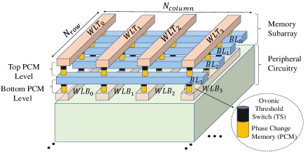
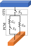
Fig. 1 shows the overall structure of a 3D XPoint subarray. A two-level PCM stack is integrated at the top of CMOS peripheral circuitry. The storage device is based on phase-change memory (PCM) technology, which is connected to a compatible ovonic threshold switch (OTS) made of AsTeGeSiN [12, 13, 14]. Word lines at the top (s), word lines at the bottom (s), and bit lines (s) in the middle provide the current path to each individual memory cell [15]. The compatibility of the junction of PCM and OTS devices is a key factor in allowing access to individual cells without facing sneak path problems [16]. The total number of PCM cells in the 3D XPoint subarray with rows and columns is , with half in the top PCM level and half in the bottom PCM level, as shown in the figure.
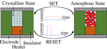
PCM is a non-volatile memory technology exploiting Ge–Sb–Te (GST) alloys (e.g., Ge2Sb2Te5) as the storage medium [17]. PCM has two states: a crystalline phase with high conductance () and an amorphous phase with low conductance (). The GST alloy transition between amorphous and crystalline states is triggered by changing the temperature level [18, 19]. In early explorations of PCM technology (1970s–early 2000s), the temperature level was changed using a laser source [20]. The state-of-the-art research on PCM is focused on using electrical impulses to change the temperature, and hence the state, of the PCM device by applying an electric current (or voltage) pulse across the PCM device [21].
Fig. 2(a) shows that applying a fast high-amplitude current pulse of amplitude (called the RESET pulse) heats up the GST material to the melting temperature (600∘C or higher [19]), erasing the previous periodic and ordered atomic arrangement. After quenching, the new disordered atomic structure will be frozen, making the transition from high conductance crystalline state to low conductance amorphous state possible. To change the state of the GTS from amorphous to crystalline, a slow, relatively low amplitude current pulse of amplitude (called the SET pulse) must pass through the GST material. The SET current pulse causes the GST material to heat up to crystalline temperature (400∘C [19]). Over a long SET time of several tens of nanoseconds, this is a high enough temperature (still lower than ) for the reconfiguration and crystallization of the previous amorphous atomic region to the crystalline state. The desirable PCM characteristics are a lower amplitude of the RESET current and a shorter SET time. A RESET current as low as 10A and a SET time as low as 25ns for individual PCM devices is already demonstrated with sub-20nm scalability, high endurance 1012 cycles, and a projected 10-year retention time at 210∘C [22].
Fig. 2(b) shows the electrical model of PCM cell. The resistance across the PCM cell can be modeled by two voltage controlled switches [7]. Depending on the status of switches and , different currents flow between two lines connected to the terminals of the PCM cell, determined by and . The ON/OFF states of the memory cell are determined by OTS: If the voltage level across the OTS of a cell is larger than a threshold, the cell is considered to be ON, and it is OFF otherwise. In today’s technologies, the OTS conductance for the OFF state is up to smaller than for the ON state.
The value stored in the PCM device can represent either logic 1 (crystalline phase) or logic 0 (amorphous phase). Three memory operations available in 3D XPoint: write logic 1 (using the fast high-amplitude SET pulse), write logic 0 (using long low-amplitude RESET pulse), and read. For the memory read operation, since it is undesirable to change the state of the PCM cell, a pulse with relatively very small amplitude will be applied, increasing the temperature slightly above the ambient temperature but below (and of course ).
III Realization of In-Memory Computing
III-A Implementation of TMVM
TMVM is a fundamental step in the implementation of many applications, and is a fundamental computational kernel in machine learning (ML) applications. Using 3D XPoint as the TMVM computation engine can tremendously decrease the ML computational workload, as the data does not need to leave the 3D XPoint array during the computation.
To show how the first step of a TMVM, let us multiply, without thresholding, matrix and vector , where is given by:
| (1) |
This computes ) where each element of vector is a dot product. For example,
| (2) |
This is computed in the 3D XPoint array by applying voltages across a set of conductances to produce a current .
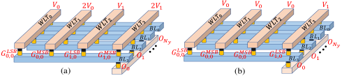
Today’s PCM cells can only store binary values. Hence, we assume that elements of matrix and vector are binary. To implement a \sayneuron-like operation using TMVM, the value and computed values are followed a thresholding operation. In (2), if the sum of products exceeds the current required to flip the output bit, then logic 1 is stored as the conductance, , of the PCM cell ; otherwise, the stored logic value is 0. Similarly, for other s, the values after thresholding are stored as the conductance states, .
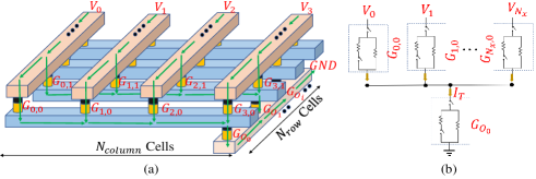
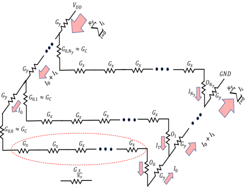
Fig. 3(a) shows the implementation of the TMVM on a 3D XPoint subarray with PCM cells ( cells each at top PCM level and bottom PCM level) where and . For clarity, as compared to Fig. 1, only the lines and PCM cells engaged in the computation are shown, and the rest of the lines and the PCM cells (at the bottom) are removed from the figure. All elements of will be calculated simultaneously and are stored in the same column with PCM cells. Considering that today’s 3D XPoint cannot store multiple values in a cell, we assume that elements of vector and are binary.
The conductances are first programmed in the top PCM level by memory write operations or by previous computation.
-
•
Before the computation starts, cells that store s at the bottom are preset to logic 0.
-
•
Then, voltages are applied to the word lines s connected to input cells located at top. If represents logic 1, voltage is applied () to the and the current that flows through the corresponding input cell is proportional to .
-
•
If represents logic 0, is floated ( float) and no current passes through the corresponding PCM cell.
-
•
The summation of currents () from input cells flows through the in a time interval . Based on the values of and , different currents pass through the input cells that store . If , the state of changes to logic 1. However, we require to avoid erroneous computation.
To calculate the minimum and maximum allowable applied voltage () to the lines, we consider a simplified electrical model for the implementation of a dot product (e.g., for ) shown in Fig. 3(b). Current can be written as follows
| (3) |
When the computation begins, since the preset is 0, and is small (of the order of few hundred nAs). However, by the passage of time, the amorphous region near the heater in the output PCM starts to turn crystalline, resulting in increasing (and consequently ) and heat (generated by the flow of more electric current). If the applied voltage is large enough to provide a current larger than , crystallization repeats until a threshold point where the whole amorphous region in the output PCM turns into a crystalline region with high conductivity, representing logic 1. On the other hand, the must not be so large that the generated temperature exceeds , causing erroneous computation.
To calculate the range for the accurate implementation of the described dot product, we analyze the two cases corresponding to (the minimum acceptable voltage) and (the maximum acceptable voltage). For the case, we assume that all s, and all s represent logic 1, i.e., voltages are applied to all s and the conductances of input cells are in the high conductance state corresponding to . In this case, from (3), . Since , the requirement implies a first constraint, requiring that to lie in the range:
| (4) |
For the case, all s are set to logic 1, while all s are set to logic 0. Since the result of the dot product should be at logic 0, we expect that the preset value of PCM stored remains intact. At the maximum voltage possible, we hypothetically assume that the applied voltage pulse should be below the level required to change the output state from logic 0 to logic 1, even if conductances of all input cells are . In other words, , i.e., the output state cannot be altered. Therefore, the second set of constraints require to lie in the range
| (5) |
The acceptable range for is . Therefore, the minimum and maximum acceptable voltages are and , respectively.
III-B Implementation of NN
Using the TMVM implementation, we implement a neuromorphic inference engine. Fig. 4(a) shows a single-layer NN with inputs and outputs. Fig. 4(b) shows the data layout for the NN implementation on a 3D XPoint subarray. The top PCM cells are allocated for storing the weights (s), similar to s in TMVM that were stored in the top PCM cells, and the bottom PCM cells are allocated for storing the outputs (s), similar to in TMVM. The inputs (s) are applied to s as voltage pulses (similar to s in TMVM).If and , then all s can be determined simultaneously in one step. The output elements of the NN can be stored in any column at the bottom (here, we choose column 1). In Fig. 4(b), all other cells at the bottom patterned by diagonal stripes are not engaged in the computation of s, i.e., s connected to these cells are floated.
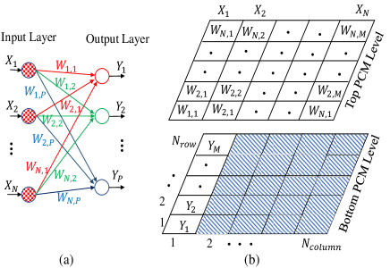
An application for the proposed NN implementation is handwritten digit recognition of MNIST dataset with 10K test images [23]. Analyzing each MNIST test image can be performed using a similar NN shown in Fig. 4(a). Here , as in MNIST each image represents a digit (from 0 to 9). In each computational step, images can be processed and stored in a column.
IV Enabling More Complex Implementations
In this section, we discuss three concepts that enable more complex computations. Then, we provide the implementation of a multi-layer NN as an example.
IV-A 3D XPoint with four stacked level of PCM cells
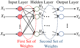
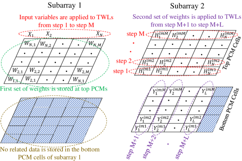
Industry projections show that the next generation of 3D XPoint will have four-level stacked PCM cells [24]. If the number of PCM levels increases, then the volume of stored information per footprint area increases, and more complex implementations are possible. Although a two-level subarray of PCM cells is sufficient to implement any NN (see Section IVD), we will illustrate how we can use a four-level subarray of PCM cells to implement a multi-layer NN by exploiting the extra PCM levels. The NN in Fig. 5 has three layers: an input layer, a hidden layer, and an output layer. At the top PCM level, the first set of weights are stored. In the next PCM level, the hidden layer data is calculated, and by applying the second set of weights as voltage pulses, we obtain the outputs of the NN at the third PCM level.
IV-B Scalability of 3D XPoint to large computations
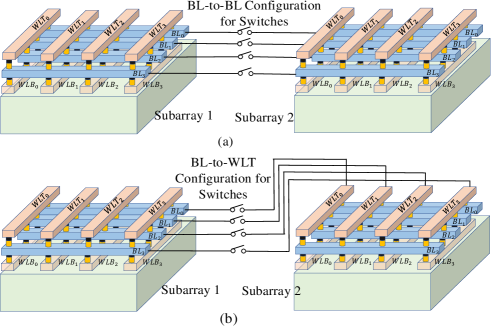
We can connect multiple 3D XPoint subarrays to create a larger array to handle computations with higher matrix dimensions. In Fig. 6(a), switches connect s of subarray 1 to those of subarray 2, enabling current flow from the s of subarray 1 to those of subarray 2. The of subarray 2 that is scheduled to store the computation results will be connected to ground, while all other s not engaging in the computation (in both subarrays 1 and 2) are floated. Hence, the computation results in subarray 1, are being calculated and stored at the bottom PCM level of subarray 2 (-to-). In Fig. 6(b), switches connect s of the subarray 1 to of subarray 2. In this configuration, the results are being calculated at the top PCM level of subarray 2. The status of lines during the computation for these two configurations are listed in the Supplementary Materials.
IV-C Multi-bit operations
Thus far, we have discussed the implementations of operations with binary digits. We introduce two methods that enable us to implement operations with multi-bit digits. For brevity, we explain the principle using two-bit digits, where each digit consists an (most significant bit) and an (least significant bit). Let us assume that we want to perform TMVM of where is a matrix with two-bit elements, meaning the element located in row and column of the matrix is .
Fig. 7 illustrates two ways to implement 2-bit operations on a 3D XPoint subarray. Fig. 7(a) shows an area-efficient approach. For example, to calculate , we need to calculate . To do so, we can apply to the (connected to the PCM storing bit), and we can apply to (connected to the PCM storing bit). Therefore, the current flowing through the cell is two times larger than that of the cell. Another more area-intensive approach, which does not require multiple voltage levels, is shown in Fig. 7(b) where we copy the in pair of adjacent cells, and we apply the same voltage to their corresponding s. The current through the cell is weighted to be twice that of the current through the cell.
IV-D Multi-layer NN implementation in a two-level PCM stack
We now illustrate how a multi-layer NN can be implemented using a three-layer PCM stack. As an example, we discuss the implementation of the three-layer NN (shown in Fig. 5) using two two-level 3D XPoint subarrays. Let us assume that the NN is required to analyze 10K images of the MNIST dataset. The data layout of this implementation is illustrated in Fig. 8 using two subarrays connected with -to- configuration (see Fig. 6(b)). The first set of weights is stored at the top PCM cells of subarray 1. The inputs () are applied as the voltages to the s of subarray 1. We assume that at each time step, the hidden layer values () for a specific image from MNIST are being processed. For example, the hidden layer values of the second image () is calculated in step 2. Assuming that we calculate the hidden layer values of () images in each set of computation, we require steps to calculate and store the hidden layer values of images at the top PCM cells of subarray 2. In each of these steps, the corresponding in subarray 2 is connected to , and the remaining s in subarray 2 are floated. After all hidden layer values are stored at the top PCM cells of subarray 2, we apply the second set of the weights (as voltage pulses) to the s of subarray 2. At each column at the bottom PCM cells of subarray 2, the outputs (s) of images are calculated and stored.
V Analyzing Interconnect Parasitic Effects
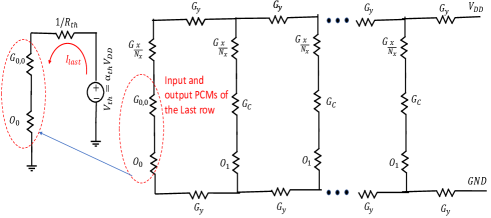
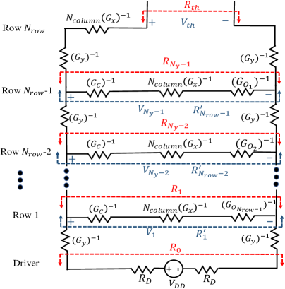
To ensure the electrical correctness of the implementations in in-memory computing platforms, we must consider non-idealities due to wire parasitic effects [10, 11]. As an example, we consider the implementation of a TMVM illustrated in Fig. 3(a). In thhe equivalent circuit model shown in Fig. 9, the s, s, and s have nonzero parasitics that cause a voltage drop in the current path across the 3D XPoint subarray, that may potentially lead to errors in the results of TMVM. Let and be the conductances of the segments of s and s, respectively. The conductances for and are considered equal (both ) due to the symmetry and equal allocation of metal resources to s and s. We use to denote the conductance of PCM cell () at the top level, and s to denote conductances of a column of PCM cells at the bottom level. In the worst case, each row performs an identical operation, and carries an equal current . The total voltage drop to the last row is
| (6) |
where the first, second, and last terms on the left side of the equation are for voltage drops of , , and , respectively. The voltage drop of the last row increases quadratically with the number of rows, and this causes a significant limit on the accuracy of the implementations [10, 11]. Hence, it is important to find the maximum allowable subarray size in which the voltage drop does not impair the electrical of implementations.
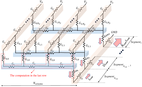
During the computation, the resistive network shown in Fig. 9 can have different configurations based on the applied voltage to s. For example, if float, then all s and their connected parasitics must be removed from the equivalent circuit model of Fig. 9. To analyze parasitic effects, we consider the corner case for voltage drop, where only and the rest of the s are floated, resulting in minimum equivalent conductance for inputs and wire parasitics. Moreover, for the corner case, we assume that inputs and outputs are located columns away from each other (the farthest possible distance). The value of all inputs assumed to be 1, and therefore, the current flows from the inputs of the TMVM computation must be sufficient enough to change the state of the output of the TMVM computation. An excessive voltage drop across the input and output cells causes a failure in the TMVM implementation discussed earlier.
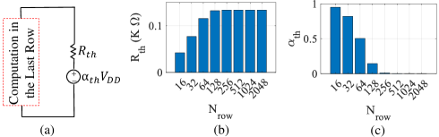
The rows far from the drivers have larger parasitics between them and the driver. In particular, for the last row (farthest from the driver, see Fig. 9), the voltage drop is the worst. If the electrical correctness for the last row does not hold up, the implementations would be unacceptable. We observe the rest of the circuit from the last row and calculate (for the worst case) the Thevenin resistance () and Thevenin voltage () (see Fig. 10(a)). We define the Thevenin coefficient, , and its value is between 0 and 1. Both and can be obtained analytically using a recursive approach explained in Appendix Exploring the Feasibility of Using 3D XPoint as an In-Memory Computing Accelerator. Both are functions of parameters such as , , PCM cell width () and length () as well as other parameters of PCM and wire devices. Fig. 10(b) and (c) shows and for different values. The configuration of lines are based on configuration 1 that will be discussed in Table I in the next Section.
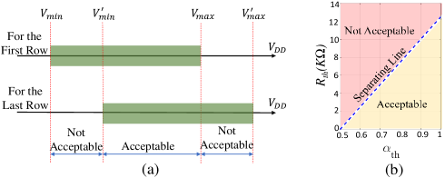
There are negligible parasitics between the first row and the driver, and the voltage range that ensures accuracy of computing in the first row is closer to (discussed in Section III) than that of the last row. For the last row, values of and are significantly affected by parasitics. Let us assume that the new voltage range ensures electrical correctness of the last row is . The voltage ranges for the first row and last row are shown in Fig. 11(a). We use the voltage ranges of first row and last row as two corner cases (with least and most voltage drops, respectively), and we find a voltage range the satisfy both corner cases; the obtained voltage range guarantees the electrical correctness for intermediate rows as well. The final acceptable voltage range is the overlap between two voltage ranges shown in Fig. 11(a), , ensuring all of the rows from first row to the last row receiving the proper voltage.
The noise margin () in implementations is defined by
| (7) |
where . Clearly, we desire . In Fig. 11(b), the acceptable and unacceptable regions in the () plane is shown. The on the separating line is 0, above it is negative (unacceptable), and below it is positive (acceptable). Our goal is to choose wire configurations so that the corresponding () of the design falls into the acceptable region with maximum possible.
VI Results and Discussion
VI-A NM evaluation
![[Uncaptioned image]](/html/2106.08402/assets/x15.png)
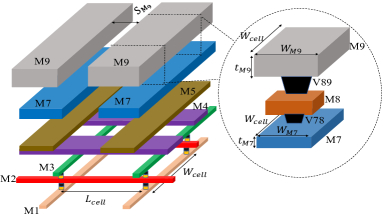
To realistically analyze the effect of the parasitics, we assumed that metal layers in 3D XPoint are constructed based on ASAP7 design rules [25, 26] (see Fig. 12). We can create different configurations for allocating metal lines to s, s, and s. Table I lists three possible configurations. In configuration 1, only M1, M2, and M3 (the first three metal lines) in ASAP7 are exploited for 3D XPoint, and they are allocated to , , and , respectively. For configurations 2 and 3, we assume that other than M1, M2, and M3, the other metal layers (M4 to M9) can also be allocated to the 3D XPoint lines. In configuration 2, we allocate M4 and M5 to the s, and M6 to M9 are allocated equally between s and s. In configuration 3, we assume that all metals from M4 to M9 are allocated equally between s and s; no extra top metal lines are allocated to s. We report the minimum cell width () and length () for each configuration based on the minimum required width of a line and space between adjacent lines in each layer. The values of parameters for metal lines and PCM devices are available in the Supplementary Material.
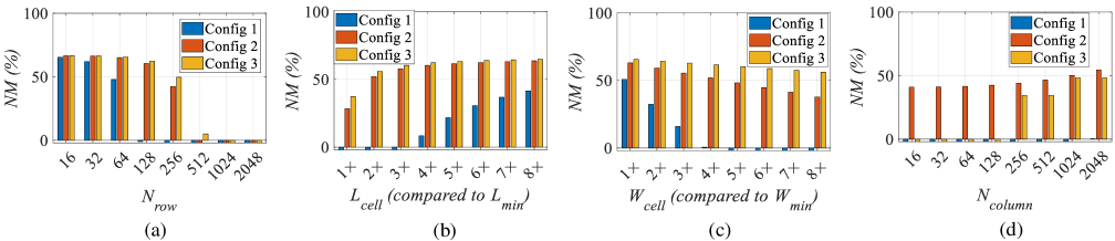
improves with increasing : Fig. 13(a) shows s of different values. is significantly sensitive to . For as large as 2048, the implementations are not valid due to excessive voltage drop, and hence negative . Configuration 3 provides the best , because more metal resources dedicated to and causes smaller parasitics in the current path across rows.
improves with increasing : Fig. 13(b) shows the s for different s (for each configuration, values are normalized to listed in Table I). By increasing , the width of the s and s increase, decreasing the parasitic resistances related to s and s.
decreases with increasing : Fig. 13(c) shows the s for different (for each configuration, values are normalized to listed in Table I). By increasing , the length of the s and s increase, and consequently, parasitics related to s and s considerably increase. Therefore, for all cases, smaller causes larger .
remains unchanged with increasing : Fig. 13(d) shows that the increase in does not affect significantly. By increasing , parasitics of s increase. However, since the resistances are in series with those of PCM devices with orders of magnitude larger resistance, the increase in resistance does not affect .
VI-B Implementing NNs on the 3D XPoint substrate
We list the performance of various 3D XPoint subarrays of various sizes for the digit recognition of MNIST dataset in Table II. Each MNIST test image is scaled to 1111 as in [27], a transformation that maintains 91% recognition accuracy and reduces computation. We use configuration 3 in all cases, as it provides the best among all alternatives. For the smallest subarray with size , is the maximum among all cases. For the largest subarray with size , we increase by 2.6 (compare to that of subarray) to decrease the parasitics of lines. Consequently, we achieve acceptable of . With this relatively large subarray, we have more parallelism that allow to process a larger number of MNIST images in each computational step, reducing the total execution time (17 faster than that of 64128 subarray). The energy per image is similar for all cases because the subarray sizes listed in Table II are large enough to allow fully processing an 1111 MNIST image locally without the need for extra data movement between subarrays or peripheral circuitry.
We analyze the energy and area for the implementation a multi-bit TMVM using two schemes that we introduced in Section IVD. We listed the results in Table III. As we increase the number of bits for the s, the allocated area for both implementations increases. However, while for area-efficient scheme, the area increases linearly, for the low-power scheme, the area increases exponentially. The implementation energy in the low-power scheme slightly increases with increasing the number of bits, while for the area-efficient schemes, energy increases rapidly. For the area-efficient scheme, we do not list the energy and area values beyond 3 bits, because it requires applying a large voltage level (5V) within the subarray, making the implementation infeasible and unrealistic.
![[Uncaptioned image]](/html/2106.08402/assets/x16.png)
![[Uncaptioned image]](/html/2106.08402/assets/x17.png)
VII Conclusion
We have presented methods for the implementations of TMVM, NN, and 2D convolution on 3D XPoint. To ensure the accuracy of the implementations, we considered wire parasitics in our implementations. We have demonstrated that interconnect parasitics have a significant effect on the implementations performance and have developed a comprehensive model for analyzing this impact. Using this methodology, we have developed guidelines for the 3D XPoint Subarray size and configurations based on ASAP7 technology design rules. We used different size 3D XPoint subarrays for digit recognition of MNIST dataset. Using the our methodology methodology, we design a relatively large subarray of 2 Mb with acceptable of 34.5, providing the opportunity for processing more images per step without any energy overhead.
References
- [1] A. McAfee, et al., “Big data: The management revolution,” Harvard Business Review, Oct. 2012.
- [2] S. W. Keckler, et al., “GPUs and the future of parallel computing,” IEEE Micro, vol. 31, pp. 7–17, Nov. 2011.
- [3] “3D XPoint technology.” https://www.intel.com/content/www/us/en/architecture-and-technology/intel-micron-3d-xpoint-webcast.html.
- [4] N. Agrawal, et al., “Design tradeoffs for SSD performance,” in USENIX 2008 Annual Technical Conference, p. 57–70, June 2008.
- [5] K. Son, et al., “Signal integrity design and analysis of 3-D X-Point memory considering crosstalk and IR drop for higher performance computing,” IEEE Transactions on Components and Packaging Technologies, vol. 10, pp. 858–869, May 2020.
- [6] K. Son, et al., “Modeling and verification of 3-dimensional resistive storage class memory with high speed circuits for core operation,” in IEEE Asia-Pacific Microwave Conference, pp. 694–696, Mar. 2019.
- [7] K. Son, et al., “Modeling and signal integrity analysis of 3D XPoint memory cells and interconnections with memory size variations during read operation,” in IEEE Symposium on Electromagnetic Compatibility, Signal Integrity and Power Integrity, pp. 223–227, July 2018.
- [8] Q. Lou, et al., “3DICT: A reliable and QoS capable mobile process-in-memory architecture for lookup-based CNNs in 3D XPoint ReRAMs,” in Proceedings of the IEEE/ACM International Conference on Computer-Aided Design, pp. 1–8, Jan. 2018.
- [9] J. Yang, et al., “Exploring performance characteristics of the optane 3D XPoint storage technology,” ACM Transactions on Modeling and Performance Evaluation of Computing Systems, vol. 5, Feb. 2020.
- [10] D. Ielmini and G. Pedretti, “Device and circuit architectures for in-memory computing,” Advanced Intelligent Systems, vol. 2, pp. 2000049–1–2000040–19, May 2020.
- [11] M. Zabihi, et al., “Analyzing the effects of interconnect parasitics in the STT CRAM in-memory computational platform,” IEEE Journal on Exploratory Solid-State Computational Devices and Circuits, vol. 6, pp. 71–79, June 2020.
- [12] M. Lee, et al., “Highly-scalable threshold switching select device based on chaclogenide glasses for 3D nanoscaled memory arrays,” in IEEE International Electronic Devices Meeting, pp. 2.6.1–2.6.3, Dec. 2012.
- [13] G. W. Burr, et al., “Access devices for 3D crosspoint memory,” Journal of Vacuum Science & Technology B, vol. 32, pp. 040802–1–040802–23, July 2014.
- [14] DerChang Kau, et al., “A stackable cross point phase change memory,” in IEEE International Electronic Devices Meeting, pp. 1–4, Mar. 2009.
- [15] W. Chien, et al., “A study on OTS-PCM pillar cell for 3-D stackable memory,” IEEE Transactions on Electron Devices, vol. 65, pp. 5172–5179, Nov. 2018.
- [16] L. Shi, et al., “Research progress on solutions to the sneak path issue in memristor crossbar arrays,” Nanoscale Advances, vol. 2, pp. 1811–1827, Mar. 2020.
- [17] J. Y. Wu, et al., “A low power phase change memory using thermally confined TaN/TiN bottom electrode,” in IEEE International Electronic Devices Meeting, pp. 3.2.1–3.2.4, Jan. 2011.
- [18] H. . P. Wong, et al., “Phase change memory,” Proceedings of the IEEE, vol. 98, pp. 2201–2227, Dec. 2010.
- [19] G. W. Burr, et al., “Recent progress in phase-change memory technology,” IEEE Journal on Emerging and Selected Topics in Circuits and Systems, vol. 6, pp. 146–162, June 2016.
- [20] M. Wuttig and N. Yamada, “Phase-change materials for rewriteable data storage,” Nature Materials, vol. 6, p. 824—832, Nov. 2007.
- [21] Q. Zheng, et al., “Nanoscale phase-change materials and devices,” Journal of Physics D: Applied Physics, vol. 50, p. 243002, May 2017.
- [22] M. Le Gallo and A. Sebastian, “An overview of phase-change memory device physics,” Journal of Physics D Applied Physics, vol. 53, p. 213002, May 2020.
- [23] Y. LeCun, “The MNIST database of handwritten digits.” http://yann.lecun.com/exdb/mnist/.
- [24] “3D XPoint with four-level PCM cells.” https://www.anandtech.com/show/15972/intel-previews-4layer-3d-xpoint-memory-for-secondgeneration-optane-ssds.
- [25] L. T. Clark, et al., “ASAP7: A 7-nm FinFET predictive process design kit,” Microelectronics Journal, vol. 53, pp. 105–115, July 2016.
- [26] L. T. Clark, et al., “Design flows and collateral for the ASAP7 7nm FinFET predictive process design kit,” in Proceedings of the IEEE International Conference on Microelectronic Systems Education, pp. 1–4, June 2017.
- [27] M. Liu, et al., “A scalable time-based integrate-and-fire neuromorphic core with brain-inspired leak and local lateral inhibition capabilities,” in Proceedings of the IEEE Custom Integrated Circuits Conference, pp. 1–4, July 2017.
We derive recursive expressions for calculating and of a subarray of 3D XPoint.
Within the footprint area of a cell , we define (representing the conductance for and segments) and (representing the conductance of segment). Fig. 14 shows the equivalent simplified circuit model for the implementation TMVM in the corner case. Row is separated from its predecessor by conductance at each end. The input cell is connected to the output cell, columns away. The conductances in the last row are rearranged to create a two-port structure consisting of the PCM conductances so that the rest of the network can be modeled using Thevenin Equivalents ( and ).
For configuration 1 (listed in Table I), (assuming similar wire conductance for s and s) and in which the conductance, , is given by: , where , , , and are, respectively, the resistivity, length, thickness, and width in metal layer (see the Supplementary Material). For configurations 2 and 3, the equivalent conductance of the wire segment must be calculated based on the multi-metal layer configuration of a given segment. For example, in configuration 2, (representing a segment conductance of ) is obtained by .
To calculate and , we derive recursive expressions. For conciseness, we define the resistance, , of row as:
| (8) |
We can obtain , using the notations in Fig. 14, as:
| (9) |
where is calculated using the recursive expression:
| (10) |
The base case corresponds to the driver row that precedes the first row, and is , as seen in Fig. 14.
To compute , as illustrated in Fig. 14, we first compute the intermediate variable , which corresponds to the effective downstream resistance (away from the source) seen from node . The computation proceeds in a recursive fashion from the last row towards the first as:
| (11) |
with the base case . Having computed , we may now compute , using a recursive computation on :
| (12) |
in which and the base case is:
| (13) |
Supplementary Material
-A PCM parameters
-B Interconnect specifications for ASAP7
The interconnect specifications are listed in Table V, which shows the metal thickness () and resistivity (), the minimum line spacing (), minimum line width (), and Table VI, which shows the via parameters [25, 26].
| Metal | ||||
|---|---|---|---|---|
| M1(V) | 36nm | 18nm | 18nm | 43.2.nm |
| M2(H) | 36nm | 18nm | 18nm | 43.2.nm |
| M3(V) | 36nm | 18nm | 18nm | 43.2.nm |
| M4(H) | 48nm | 24nm | 24nm | 36.9.nm |
| M5(V) | 48nm | 24nm | 24nm | 36.9.nm |
| M6(H) | 64nm | 32nm | 32nm | 32.0.nm |
| M7(V) | 64nm | 32nm | 32nm | 32.0.nm |
| M8(H) | 80nm | 40nm | 40nm | 28.8.nm |
| M9(V) | 80nm | 40nm | 40nm | 28.8.nm |
| Via | Via Size | Minimum Spacing | |
|---|---|---|---|
| V12 (M1 and M2) | 17 | 18nm18nm | 18nm |
| V23 (M2 and M3) | 17 | 18nm18nm | 18nm |
| V34 (M3 and M4) | 17 | 18nm18nm | 18nm |
| V45 (M4 and M5) | 12 | 24nm24nm | 33nm |
| V56 (M5 and M6) | 12 | 24nm24nm | 33nm |
| V67 (M6 and M7) | 8 | 32nm32nm | 45nm |
| V78 (M7 and M8) | 8 | 32nm32nm | 45nm |
| V89 (M8 and M9) | 6 | 40nm40nm | 57nm |
-C Status of lines during communications between subarrays
The status of 3D XPoint lines during the communications with each other is listed in Table VII.
| Line | Subarray | Configuration | ||
|---|---|---|---|---|
| BL-to-BL | BL-to-WLT | |||
| s | 1 | s are applied | are applied | |
| 2 | all float | all active | ||
| s | 1 | all active | all active | |
| 2 | all active |
|
||
| s | 1 | all float | all float | |
| 2 |
|
all float | ||
-D Corner case circuit
The corner case circuit is shown in Fig. 15. In the Appendix Exploring the Feasibility of Using 3D XPoint as an In-Memory Computing Accelerator, we simplified the circuit even further and calculate the Thevenine equvalents observed from the last row. In Fig. 16, we show the reconfiguration and simplification of circuit shown in Fig. 15.