Characterization and Modeling of Self-Heating in Nanometer Bulk-CMOS at Cryogenic Temperatures
Abstract
This work presents a self-heating study of a 40-nm bulk-CMOS technology in the ambient temperature range from down to . A custom test chip was designed and fabricated for measuring both the temperature rise in the MOSFET channel and in the surrounding silicon substrate, using the gate resistance and silicon diodes as sensors, respectively. Since self-heating depends on factors such as device geometry and power density, the test structure characterized in this work was specifically designed to resemble actual devices used in cryogenic qubit control ICs. Severe self-heating was observed at deep-cryogenic ambient temperatures, resulting in a channel temperature rise exceeding and having an impact detectable at a distance of up to from the device. By extracting the thermal resistance from measured data at different temperatures, it was shown that a simple model is able to accurately predict channel temperatures over the full ambient temperature range from deep-cryogenic to room temperature. The results and modeling presented in this work contribute towards the full self-heating-aware IC design-flow required for the reliable design and operation of cryo-CMOS circuits.
I Introduction
Quantum computers have the potential to solve certain computational problems that would otherwise take a prohibitive long time to complete using classical computers. For proper operation, the quantum bits (qubits) –the basic unit of information in quantum computers– need to be cooled down to deep-cryogenic temperatures, around a few Kelvin in some cases [1] but typically below [2]. Since state-of-the-art quantum computers comprise only a handful of qubits, each qubit can be individually wired to equipment placed at room temperature (RT)[3]. However, to be of any practical use, future quantum computers require thousands to even millions of physical qubits, making today’s approach unworkable due to the need for thousands of cables going from the cryogenic qubits to the RT equipment. The problems associated with scalability, manufacturability and reliability of these systems could be solved by placing integrated control electronics in close vicinity to the qubits, thus requiring electronic circuits operating at cryogenic temperatures. Such electronics are typically operated at liquid helium (LHe, ) temperature, as commonly-adopted dilution refrigerators can offer significant cooling power ( ) [4] only at those temperatures.
The technology of choice for the cryogenic controller is nanometer CMOS, for its high speed, maturity, integration density and its potential to operate down to [5, 6], all required for handling a large number of qubits.
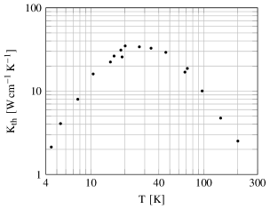
It has been shown that core device parameters, such as threshold voltage, mobility, subthreshold slope, mismatch and leakage, can shift significantly from their RT values at low ambient temperatures () [7, 8, 9, 5, 10]. The incorporation of device temperature in compact models extended to the cryogenic environment is thus paramount to guarantee reliable circuit simulations and hence, robust circuit operation under these conditions. However, self-heating (SH) can raise the device temperature () significantly above . This effect is amplified at cryogenic temperatures, as thermal properties of silicon, such as thermal conductivity (), vary almost over 1.5 orders of magnitude in the temperature range from RT down to , as shown in Fig. 1.
For instance, a recent cryo-CMOS microwave driver for spin qubits operating at = was subjected to SH exceeding for a dissipated power above [12].
SH does not only impact the characteristics of the device itself, it can also propagate through the surrounding silicon forming thermal feedback loops with neighboring devices [13]. While this can be already critical in electronic cryogenic circuits, it will become crucial in future system-on-chip (SoC), integrating both electronics and qubits, which are extremely sensitive to any thermal crosstalk [1].
SH at RT has received much attention in literature, specifically focused on silicon-on-insulator (SOI) technologies as the buried oxide (BOX) poses a thermal impedance 2 orders of magnitude higher compared to that of bulk silicon at this temperature [11, 14].
Far less attention was devoted to studies on SH at cryogenic temperatures. Early work dates back to the beginning 1970s [15] and has been extended more recently by investigations on bulk MOSFETs [15, 16, 17, 13, 18], resistors [19, 20] and SOI [21, 22]. SH was investigated both by measurements of the device temperature itself [21, 22, 20] and by placing temperature sensors in the vicinity of on-chip heaters [13, 19, 23, 24, 25, 20]. All these works show that SH is exacerbated at cryogenic temperatures and that the effect is highly dependent on device geometry (size, aspect ratio) and power density. This variability is clearly observed in recent cryo-CMOS integrated circuits for qubit interfacing, as SH ranged from 1 to in a 40-nm bulk-CMOS high-speed ADC [26] to more than in a 22-nm FinFET microwave driver [12]. As device geometry and power density differ considerably between advanced bulk CMOS nodes and the previously studied mature technologies, it is necessary from a modeling perspective to characterize SH on devices better resembling those employed in practical cryo-CMOS designs [27, 26, 28, 29], both in geometry and power density. Understanding the impact of SH is especially crucial for the cryo-CMOS low-noise amplifiers (LNA) necessary for the detection of the weak signals from quantum processors, as an increase of the device temperature of only a few Kelvin can strongly affect the noise performance, e.g., in a thermal-noise-limited amplifier in which the noise is directly proportional to the device temperature.
This paper bridges this gap by characterizing and modeling the effects of SH on the device itself and on the surrounding silicon, using a typical NMOS device.
It is found that SH can have a severe impact on both the device operating temperature and the temperature of the surrounding silicon at deep-cryogenic temperatures, and, that the former effect can be be successfully predicted using a simple modeling approach.
This paper is structured as follows: Section II describes the test chip, measurement setup and the device calibration. Section III presents the measurement results, which are discussed and modeled in Section IV. Finally, conclusions are drawn in Section V.
II Test Structures and Measurement Setup
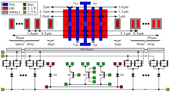
A test chip was taped-out, specifically designed for the characterization of SH at deep-cryogenic temperatures. The chip was manufactured in the TSMC 40-nm bulk-CMOS process. Fig. 2 and Fig. 3e show a simplified overview of the test structures and a die micrograph, respectively.
Three NMOS devices are employed as heaters (H1, H2 and H3), formed by a 5 fingered device with fingers measuring each, individually selectable (separated gates and drains) and able to dissipate of power. The gates of the two MOSFETs separating H1 and H3 from H2 are connected to in order to electrically isolate the heaters from each other (Fig. 2 top). The center heater (H2) has additional connections available, enabling the measurement of the gate resistance, further discussed in Section II-A. The choice for NMOS over a PMOS device was motivated by its higher current driving capability (and thus power), as no significant thermal differences are expected between both types.
In addition to the MOSFETs, a linear array comprising 52 diodes is placed perpendicular to the channel, along a line through the center of the heaters (Fig. 2 top). These diodes act as temperature sensors, enabling the detection of the spatial thermal profile in the heaters’ vicinity, further discussed in Section II-B.
II-A Gate Test Structure
To enable characterization through a range of , gate thermometry is employed, in which the calibrated temperature dependence of the gate resistance (, see Section II-D) is used as a temperature sensor [22, 30]. Kelvin connections to both top (, ) and bottom (, ) side of the H2 gate are therefore available to mitigate the impact of temperature dependence of back-end metals and parasitics on the resistance measurement (see Fig. 2).
The assumption was made that the gate and the channel are tightly thermally coupled, since only a thin (¡ ) insulating layer separates them: .
II-B Diode Test Structures
For the measurement of the thermal profile around the heaters, the substrate temperature is sensed by measuring the calibrated thermal dependency of the voltage drop () across /NWELL silicon diodes operated at a constant current . A graphical representation of this structure can be seen in Fig. 2, comprising pad-accessible diodes and a multiplexed diode array.
Pad-accessible diodes: two diodes (D1 and D2 in Fig. 2) are placed in close vicinity to the heaters (one on each side), with connections directly available via bond pads, to measure
the substrate temperature at small distances from the heaters with high spatial resolution (). Different combinations of heaters (H1/H2/H3) and diodes (D1/D2) allow for a total set of 6 distances: = {1, 1.3, 1.6, 2, 2.3, 2.6} .
Because of the direct connection to the pads, these diodes have been used as benchmark to verify the correct operation of the pass gates in the multiplexed diode array.
Multiplexed diode array: a multiplexed array comprising 50 diodes to characterize the substrate temperature over larger distances, up to from the heaters, enables automatic characterization. Thick-oxide pass gates were employed to allow the diode potential to rise above the nominal supply voltage (), required as increases with decreasing temperature.
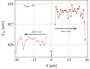
An array was placed on both sides of the heaters. The ‘dense’ array (Fig. 2 top right) comprises diodes placed at the minimum allowed distance, resulting in a spatial resolution of and is used for the actual measurements. The ‘sparse’ array (Fig. 2 top left) is a copy of the ‘dense’ array with every other device removed, resulting in less contact/metal density compared to the latter array. By comparing the results from the two arrays, it can be verified if the metal/contact density significantly impacts the thermal profile due to heat-leakage via the biasing metal lines.
II-C Measurement Setup
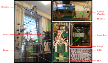
A photographic overview of the measurement setup can be seen in Fig. 3. The dies were glued and wire-bonded to ceramic DIP packages, which were fitted in a socket on a PCB mounted at the end of a dipstick (Fig. 3c). The PCB contains relays, enabling different configurations to be switched in and out during characterization. A Cernox type Resistance Temperature Detector (RTD) clamped to the package was used to measure .
Measurements at RT were carried out by inserting the end of the dipstick into a Vötsch VTM7004 climate chamber (Fig. 3b). The PCB inside the climate chamber was enclosed by a metal box to improve thermal stability, thus reducing temperature drift/gradients over time (Fig. 3d).
The dipstick was inserted into a dewar containing LHe for the cryogenic measurements (Fig. 3a). The height of the sample above the LHe level modulates .
Electrical characterization was carried out by 3 Keithley 2636B SMUs.
II-D Calibration
The temperature characteristics of both the gate resistor and the silicon diodes need to be calibrated before they can serve as temperature sensors. During calibration, the parameters of interest ( and ) as a function of are characterized while is slowly varied with all heaters disabled.
For RT, the climate chamber is used to generate a slowly varying : after warming up to , the climate chamber is switched off and allowed to (slowly) cool down while calibration takes place. Cryogenic calibration was carried out by manually lowering the dipstick into the dewar, cooling down the sample.
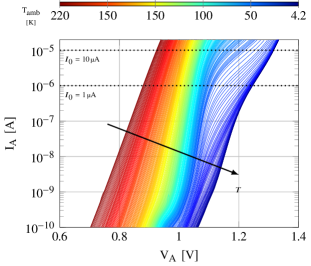
Diode Calibration: for the 2 pad-accessible diodes, the - curves are measured as a function of . Deviation from ideal exponential behavior at cryogenic temperatures can be observed in Fig. 4. From these curves, as a function of is subsequently extracted by a horizontal cut along the line = as indicated in the figure. As recording the full - characteristics for all 50 diodes in the array would take a prohibitive amount of time, is directly measured by forcing = for these devices. Since there is some variability present among different diodes, all diodes need to be calibrated individually, see Fig. 5.
An example of a diode calibration curve and the resulting temperature sensitivity can be observed in Fig. 6 top and bottom, respectively.
The de-facto standard value (for commercial diode temperature sensors) of = was used for RT. To increase the sensitivity at deep-cryogenic temperatures, the current bias was reduced to = for ¡ . The maximum temperature drift () during a single - characterization was ( RT) and ( ¡ RT).
Gate Calibration: is measured by setting and simultaneously sweeping from 0 to , see Fig. 2, while recording the current through the gate (). Note that was left open to avoid any current and consequent heating in the device. is extracted from the slope of a first-order fit of the - characteristic. The full gate calibration curve can be observed in Fig. 6 top. The maximum during a single characterization was ( RT) and ( ¡ RT).
The gap between and results from limitations in the minimum and maximum attainable temperature of the climate chamber and LHe dewar, respectively.
III Experimental Results
This section presents the measurement results, focusing on the experimental methods and discussing data validity. In-depth analysis and discussion of the reported data is given in Section IV.
III-A Gate-resistance Measurements
In the first step of the characterization, the sample is brought to the target by placing it at a certain height above the LHe level, or for RT measurements, by keeping it inside the (switched-off) climate chamber. When stays within of the set point, thermalization is assumed and different power levels are dissipated in the center heater () by stepping in a staircase pattern: = {0, 0.05, 0.1, …, 1.1} , while and are both set to . Following each step in , a delay was added to allow the structure to reach thermal equilibrium. is subsequently swept from 1.1 to , while both and are recorded. Finally, the routine
described above is repeated for multiple .
is extracted from the - data as per the calibration routine described in Section II-D. The is inferred from these extracted values by local Taylor-expansion of the calibration curve (Fig. 6 top) around that operating point.
As one side of the gate () experiences a voltage change of during measurement, increases slightly. The dissipated power is therefore calculated using the mean , , resulting in a maximum error of in power.
The absolute as a function of for different is plotted in Fig. 7. The channel self-heating, , is derived from these data by subtracting the extracted temperature at for each from the corresponding curve, as shown in Fig. 8. As the temperature sensitivity of drops to very low values for , the RTD temperature reading was used for compensation instead of for these curves.
In order to protect against sudden temperature changes in the helium vapour (caused by varying pressure in the building’s helium recovery system), the readings of the RTD are monitored: measurements are discarded when exceeds during a gate measurement at a single set point. In addition, these readings are also cross-checked with the extracted as an additional safeguard.
III-B Diode Measurements
The diode characterization is very similar to that of the gate (Section III-A); however, apart from H2, in this case, H1 and H3 can additionally be used as heaters.
The characterization and analysis of the diode measurements can again be split into two groups:
Pad-accessible diodes: , power dissipation and thermalization are handled as per the gate measurements. For each set point, is swept while and are recorded. These data are collected for all 6 combinations of H1, H2 or H3 with D1 or D2 over all targets. From the - data, is extracted in the same manner as during diode calibration and the diode temperature () is inferred with the use of the individual diode calibration curves (Fig. 6 top).
The absolute for = RT and as a function of the enabled heater and the heater power can be seen in Fig. 9.
Finally, the substrate heating (Fig. 10) is calculated by compensating each absolute temperature curve in Fig. 9 with the corresponding temperature extracted at , identical to the procedure followed in the channel SH analysis, while for the temperature reading of the RTD was used.
Multiplexed diode array: the measurement and analysis of the diode array follow the same routine as the pad-accessible diodes described above; however, due to the large number of devices (50), resulting in an increased measurement time, some adaptions were implemented to mitigate long-term : since sub- resolution is not required, only H2 was enabled; of each diode is directly measured by forcing = and the number of set points was reduced to the set = {0, 0.1, 0.2, …, 1.1} . With these measures in place, characterization of the full array still consumes a considerable amount of time, therefore needs to be taken into account.
Long-term temperature drift is only present for samples in helium vapour, caused by time-varying pressure in the building’s helium recovery system.
To further minimize impact, each diode in an array is fully characterized over all set points (power levels), before switching to adjacent devices. During characterization of a single diode, is assumed to be small (comparable to that of the pad-accessible diodes) as the characterization time is relatively short: . However, there is still a long-term present between diode measurements, since a full array characterization takes . Therefore, the same compensation employed in the channel and pad-accessible diode characterization is applied here, which in this case, additionally auto-zeros the drift component between individual diode measurements.
The long-term drift is assumed to be small enough to maintain , however, large enough to distort the SH measurement, the effect of which is dependent on the height above the LHe. During the full array characterization, the RTD readings are therefore used to guard against too large short- and long-term . The allowed short-term drift (during single-diode measurements) is as per the pad-accessible diode characterization, while the long-term drift must stay within of the target for the data not to be discarded.
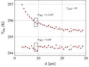
Extracted absolute substrate temperatures as a function of distance for = 0 and measured at = RT are plotted in Fig. 11.
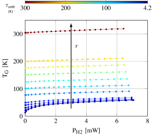
Substrate heating as a function of distance at measured at different can be observed in Fig. 12. The corresponding measured temperatures of the pad-accessible diodes and the channel have been added to the figure.
The temperature profiles associated with different heater powers at a fixed = are plotted in Fig. 13, exemplifying the effect of on a single diode measurement.
IV Self-Heating: Discussion, Modeling and Take-Aways
IV-A Diode-Based Temperature Sensing
Deviation from exponential behavior in cryogenically operated diodes shown in Fig. 4, are compatible with previous observations in literature [31, 32]. The sharp increase for ¡ can be attributed to carrier freeze-out [32, 33, 34], also present in diodes specifically designed for cryogenic temperature sensing [35].
Consistently and significantly lower were found for diodes in the ‘sparse’ array compared to the ‘dense’ array as indicated in Fig. 5. Most likely these differences can be ascribed to a combination of two effects: 1) diodes in the ‘dense’ array lie in a single continuous NWELL, while each ‘sparse’ diode sits in its own well. This causes differences in doping densities, and subsequent electrical characteristics, through the Well Proximity Effect (WPE) [36]. 2) the different Shallow Trench Isolation (STI) widths between diodes in the two arrays cause different mechanical stress to be present, altering the carrier transport parameters through the piezo-junction effect [37].
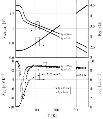
The calibration curves of and in Fig. 6 show a near-constant temperature sensitivity of and for ¿ , respectively. Freeze-out causes a large increase in sensitivity below this temperature, however, sensitivity drops to a very low value for ¡ , compatible with measurements in [34]. was reduced to during cryogenic measurements to mitigate the latter effect [31], the value being a trade-off between improved sensitivity and increased impact of array leakage at deep-cryogenic temperatures [38]. The temperature sensitivity of decreases to a value close to zero for ¡ , in-line with metal-like behavior [39]. For ¿ , carrier transport is limited by phonon scattering, exhibiting a positive temperature coefficient (PTC), while below this temperature transport becomes increasingly limited by impurity scattering, which being temperature independent, prevents further resistance decrease.
Due to the diminishing temperature sensitivity of both the diodes and gate resistance, the reading of and have been excluded for temperatures below and , respectively. However, due to the rapid temperature increase to values above already at low for = , this results in the loss of only a small part of the data (see Fig. 7 and 9).
SH due to biasing of the temperature sensors is insignificant for the range of interest ( ¿ ), as it has been simulated in COMSOL to be below for the diodes, resulting in ¡ ; and below for the gate resistor, resulting in ¡ , respectively.
IV-B Channel Temperature Sensing
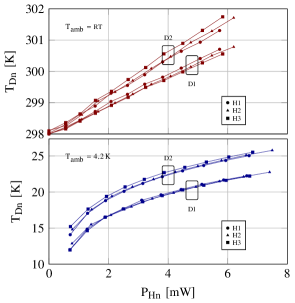
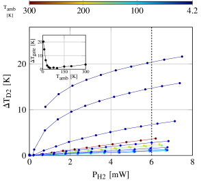
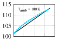
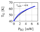
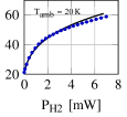
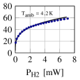
From the measurements in Fig. 7, an agreement between the RTD temperature reading and extracted was found, indicating the correct operation of the setup through the full temperature range. Larger SH at equal can be observed for lower temperatures in Fig. 8: (RT) vs () at = . For ¡ , is highly non-linear with respect to dissipated power, resulting in large SH for low in this temperature range, also observed by [24] and [18].
As shown in the inset of Fig. 8, the SH behavior from RT down to for a given shows a decrease down to , below which its effect starts to increase again, exhibiting a dramatic increase below = .
This behavior hints to a temperature-dependent , with a minimum at , also shown in other works [24, 20]. Previously reported values of the minimum lie between and and have been attributed to the impact of parasitic (package, glue, etc.) dominating at these low temperatures in bulk CMOS. The crowding of between and for deep-cryogenic temperatures, visible in Fig. 7 for heating power above , is a direct consequence of this behavior: below the minimum, has a negative temperature coefficient (NTC), which impedes SH more and more as approaches the minimum. The implications of this observed effect are further discussed in Section IV-E.
Comparing the SH magnitude extracted in this work with literature, much higher SH was found in SOI technology at comparable power densities [22]. As the main in such technology is determined by SiO2, which exceeds that of Si by 2 orders of magnitude, a large difference in SH is expected. Regarding bulk technology, in which no BOX exists, the geometry and area of MOSFET devices significantly impact SH. Far lower SH was observed in a large square heater in bulk technology [20], which has significantly more enclosing area and hence a much lower to the surrounding silicon compared to the wide/short devices measured in this work. Also, the power density is orders of magnitude less compared to that in this work. The values published on a bulk device with an aspect ratio better resembling the structures characterized in this work, but with much larger and , show a slightly smaller SH effect. The structure in question had larger area [13] and considerably lower power densities. The preliminary work done by [18] shows values that compare very well with the measurements presented here, although no geometrical details are given.
These results stress the importance of geometry on SH, which is why in this work a transistor geometry comparable to the ones employed in practical cryo-CMOS circuits was chosen.
IV-C Spatial Thermal Measurements
Observations in line with the previous two sections can be made for the pad-accessible diodes. Both diodes show a smaller compared to the at identical conditions, as the effect of heating falls off rapidly with a -law (with the distance to the heater and a factor between 1 and 2): at = , less was measured from the heater compared to itself, see Fig. 9 and 10. Again, larger at cryogenic temperatures compared to RT was observed: (RT) vs () at = , measured at from the heater.
All 6 diode/heater combinations are distinguishable at both RT and in Fig. 9, with ¿ , as D2 is closer to the heater than D1. The as a function of the enabled heater is flipped between D1 and D2, reflecting the mirror symmetry of the structure (see Fig. 2 top).
In Fig. 10, a similar behavior as in the measurements can be observed in the pad-accessible diodes below . The inset clearly shows the same behavior: a decreasing with decreasing with a minimum at , which compares well with the channel measurement.
Additional cryogenic effects were observed in the heaters, see Fig. 9. At = , the power in H1-H3 increases by to at equal bias conditions compared to RT, attributed to the improved mobility, resulting in an increased and . At equal , H2 was able to dissipate consistently more power compared to H1 and H3. H2 is effectively shielded from STI stress by adjacent devices (H1 and H3), which alters carrier transport parameters (and thus and ) through the piezo-resistive effect [37].
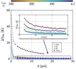
Another interesting observation on the SH structure is the heat propagation from the heaters to the ‘dense’ and ’sparse’ diode arrays. As seen in Fig. 11, there is good agreement between the in both arrays, indicating no significant effects of metal/STI density on the thermal transport for these measurements, as was described in Section II-B. The readings at correlate well with the RTD readings and an agreement within between both ‘dense’ and ‘sparse’ diodes was found at both low and high ; the latter indicates a stable and a successful calibration. The temperature mismatch between the two arrays is mainly due to the large time span between individual measurements, as each array is fully characterized before switching to the other. Compatibility of the array data with both channel and pad-accessible diode measurements can be seen, the shape corresponding to simulations shown by [20].
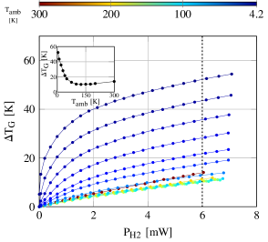
The substrate falls off with the distance from the heater for all measured , following a similar shape to measured at RT, see Fig. 12. At = , the observable range is limited as the substrate temperature drops below for , as discussed previously. The evolution over matches the pad-accessible diode data, e.g. a minimum at . At = severe substrate heating was observed, as much as , measured from the heater dissipating = .
Substrate heating at = as a function of (Fig. 13) uncovers detectable substrate heating from the heater at ¿ , while negligible heating is observed at . A short-term is visible, impacting the diode measurement at .
IV-D Ultra-Wide-Temperature Self-Heating Model
In order to make the IC design work-flow cryo-SH aware, SH was modeled via a similar approach as in [22], but for bulk CMOS. First, the differential thermal resistance () has been calculated from data in Fig. 8, and plotted as a function of absolute channel temperature () in Fig. 14. The extracted at ¡ partially overlap, proving the validity of the measured channel SH. Since SH in bulk is far less pronounced compared to SOI, and even less at higher temperatures, the range for ¿ is limited and gaps appear in the curve. The previously discussed minimum and rapid increase in SH at deep-cryogenic temperatures are also reflected in this curve. The shape of the curve, and in particular the deviation from the expected valley around , is compatible with the one shown in [20]. This curve illustrates that a single function is able to describe the complete behavior of this structure over the full temperature range from RT down to , and can thus be employed to model SH over and . As the data at deep-cryogenic temperatures are similarly shaped to those in [22], but deviates at higher temperatures (containing a minimum, not monotonically decreasing), was split into two regions, only to aid fitting. For Eq. (1) [22] was used:
IV-E SH Impact on Cryo-CMOS Circuits
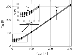
While the cryo-SH data and modeling presented above could enable the next steps in reliable cryo-CMOS design, conclusions on the impact of circuit behavior can already be drawn. Although SH is indeed severe for below (see Fig. 8), will not exceed an absolute temperature above even for a dissipated
power of a few ’s, due to the minimum in the thermal resistance, as clearly highlighted by replotting the data from Fig. 7 in Fig. 16. Since the key transistor parameters, such as threshold voltage, current factor and subthreshold slope, as well as passive-device characteristics, such as (see Fig. 6), were shown to saturate at temperatures below [8, 9], SH would not significantly impact the circuit bias conditions and its dynamic performance, causing a relative temperature insensitivity in this regime. However, the increase in circuit temperature by tens of degree Kelvin above can significantly degrade the noise performance for a thermal-noise-limited circuit, although it is still unclear whether temperature-independent shot-noise may be the main limitation in transistor’s noise performance at deep-cryogenic temperatures [40]. Moreover, since the exact position of the thermal-resistance minimum cannot be fully attributed to the thermal properties of silicon, but heavily depends on the die thermalization, such as the package, the may vary due different positions on the die or boundary conditions of the die with the surrounding enclosure. Devices at tens of distance from each other can still experience significant thermal cross-talk at deep-cryogenic temperatures even at moderate power levels ( ¿ ) within at least a radius of (see Fig. 12 and 13). This directly translates into layout guidelines to properly space power-hungry devices from noise-sensitive circuits and precision circuits for which matching is a major consideration.
V Conclusion
A 40-nm CMOS test structure was fabricated and characterized for a comprehensive evaluation of self-heating in bulk CMOS technology in the ambient temperature range from down to . The temperature rise was measured both in the MOSFET channel through the change in the gate resistance, and in the surrounding silicon substrate by a linear array of diodes operating as sensors.
Severe self-heating was observed at deep-cryogenic ambient temperatures, resulting in a channel temperature rise exceeding for a dissipated power of only at a ambient temperature. Although the thermal conductivity of silicon is relatively low at very low temperatures, the absolute channel temperature does not exceed even for significantly higher power, due to the thermal resistance for a typical MOSFET, which has minimum above . This effect was confirmed by extracting the device thermal resistance from measured data at different temperatures and modeling it with a simple analytical expression able to predict channel temperatures over the full ambient temperature range from deep-cryogenic to room temperature.
The spatial propagation of SH results in a rise in substrate temperature detectable and quantifiable at a distance of from the heater.
The thorough characterization of nanometer bulk-CMOS devices at cryogenic temperatures is of paramount importance for the design of the integrated control electronics for quantum processors. For achieving first-time-right silicon, it is imperative to simulate the circuit at the actual operating temperature rather than assume the ambient temperature. Towards that goal, the results and modeling presented in this work will contribute towards the full self-heating-aware IC design-flow required for the reliable design and operation of cryo-CMOS circuits.
Acknowledgment
The authors would like to thank Dr. H.P. Tuinhout for the helpful discussions and Intel for funding.
References
- [1] L. M. K. Vandersypen, H. Bluhm, J. S. Clarke, A. S. Dzurak, R. Ishihara, A. Morello, D. J. Reilly, L. R. Schreiber, and M. Veldhorst, “Interfacing Spin Qubits in Quantum Dots and Donors—Hot, Dense, and Coherent,” NPJ Quantum Information, vol. 3, pp. 34–44, 08 2017.
- [2] J. van Dijk, E. Charbon, and F. Sebastiano, “The Electronic Interface for Quantum Processors,” Microprocessors and Microsystems, vol. 66, pp. 90–101, 2019.
- [3] F. Arute, K. Arya, R. Babbush, D. Bacon, J. Bardin, R. Barends, R. Biswas, S. Boixo, F. Brandao, D. Buell, B. Burkett, Y. Chen, Z. Chen, B. Chiaro, R. Collins, W. Courtney, A. Dunsworth, E. Farhi, B. Foxen, and J. Martinis, “Quantum Supremacy Using a Programmable Superconducting Processor,” Nature, vol. 574, pp. 505–510, 10 2019.
- [4] F. Sebastiano, H. Homulle, B. Patra, R. Incandela, J. van Dijk, L. Song, M. Babaie, A. Vladimirescu, and E. Charbon, “Cryo-CMOS Electronic Control for Scalable Quantum Computing,” in 2017 54th ACM/EDAC/IEEE DAC, 2017, pp. 1–6.
- [5] R. M. Incandela, L. Song, H. Homulle, E. Charbon, A. Vladimirescu, and F. Sebastiano, “Characterization and Compact Modeling of Nanometer CMOS Transistors at Deep-Cryogenic Temperatures,” IEEE JEDS.
- [6] S. R. Ekanayake, T. Lehmann, A. S. Dzurak, R. G. Clark, and A. Brawley, “Characterization of SOS-CMOS FETs at Low Temperatures for the Design of Integrated Circuits for Quantum Bit Control and Readout,” IEEE TED, vol. 57, no. 2, pp. 539–547, Feb 2010.
- [7] A. Beckers, F. Jazaeri, and C. Enz, “Characterization and Modeling of 28-nm Bulk CMOS Technology Down to 4.2 K,” IEEE JEDS, vol. 6, pp. 1007–1018, 2018.
- [8] P. A. ’t Hart, M. Babaie, E. Charbon, A. Vladimirescu, and F. Sebastiano, “Characterization and Modeling of Mismatch in Cryo-CMOS,” IEEE JEDS, vol. 8, pp. 263–273, 2020.
- [9] P. A. ’t Hart, M. Babaie, E. Charbon, A. Vladimirescu, and F. Sebastiano, “Subthreshold Mismatch in Nanometer CMOS at Cryogenic Temperatures,” IEEE JEDS, vol. 8, pp. 797–806, 2020.
- [10] B. Patra, M. Mehrpoo, A. Ruffino, F. Sebastiano, E. Charbon, and M. Babaie, “Characterization and Analysis of On-Chip Microwave Passive Components at Cryogenic Temperatures,” IEEE JEDS, vol. 8, pp. 448–456, 2020.
- [11] C. J. Glassbrenner and G. A. Slack, Phys. Rev., vol. 134, pp. A1058–A1069, May 1964.
- [12] J. P. G. Van Dijk, B. Patra, S. Subramanian, X. Xue, N. Samkharadze, A. Corna, C. Jeon, F. Sheikh, E. Juarez-Hernandez, B. P. Esparza, H. Rampurawala, B. R. Carlton, S. Ravikumar, C. Nieva, S. Kim, H.-J. Lee, A. Sammak, G. Scappucci, M. Veldhorst, L. M. K. Vandersypen, E. Charbon, S. Pellerano, M. Babaie, and F. Sebastiano, “A Scalable Cryo-CMOS Controller for the Wideband Frequency-Multiplexed Control of Spin Qubits and Transmons,” IEEE JSSC, vol. 55, no. 11, pp. 2930–2946, 2020.
- [13] E. Gutierrez-D., L. Deferm, and G. Declerck, “Experimental Determination of Self-Heating in Submicrometer MOS Transistors Operated in a Liquid-Helium Ambient,” IEEE EDL, vol. 14, no. 3, pp. 152–154, 1993.
- [14] M. Asheghi, M. Touzelbaev, K. Goodson, Y. Leung, and S. Wong, “Temperature-Dependent Thermal Conductivity of Single-Crystal Silicon Layers in SOI Substrates,” J HEAT TRANSFER, vol. 120, 02 1998.
- [15] S. Sesnic and G. Craig, “Thermal Effects in JFET and MOSFET Devices at Cryogenic Temperatures,” IEEE TED, vol. 19, no. 8, pp. 933–942, 1972.
- [16] D. Foty and S. Titcomb, “Thermal Effects in n-Channel Enhancement MOSFET’s Operated at Cryogenic Temperatures,” IEEE TED, vol. 34, no. 1, pp. 107–113, 1987.
- [17] D. Foty, “Thermal Effects in p-Channel MOSFETs at Low Temperatures,” IEEE TED, vol. 36, no. 8, pp. 1542–1544, 1989.
- [18] A. Artanov, A. Cabrera-Galicia, A. Kruth, C. Degenhardt, E. Gutierrez-D, D. Durini, and S. Waasen, “Self-Heating Effect in 65nm CMOS Technology (poster),” in 2021 WOLTE14, 2021.
- [19] E. A. Gutiérrez D., L. Deferm, and G. Declerck, “Selfheating Effects in Silicon Resistors Operated at Cryogenic Ambient Temperatures,” SSE, vol. 36, no. 1, pp. 41–52, 1993.
- [20] F. De la Hidalga, M. Deen, and E. Gutierrez, “Theoretical and Experimental Characterization of Self-Heating in Silicon Integrated Devices Operating at Low Temperatures,” IEEE TED, vol. 47, no. 5, pp. 1098–1106, 2000.
- [21] J. Jomaah, G. Ghibaudo, and F. Balestra, “Analysis and Modeling of Self-Heating Effects in Thin-Film SOI MOSFETs as a Function of Temperature,” SSE, vol. 38, no. 3, pp. 615–618, 1995.
- [22] K. Triantopoulos, M. Cassé, S. Barraud, S. Haendler, E. Vincent, M. Vinet, F. Gaillard, and G. Ghibaudo, “Self-Heating Effect in FDSOI Transistors Down to Cryogenic Operation at 4.2 K,” IEEE TED, vol. 66, no. 8, pp. 3498–3505, 2019.
- [23] F. De la Hidalga-W. and E. Guttierrez-D., “The n-MOS Transistor as a Low Temperature Thermometer,” 1997.
- [24] E. A. Gutiérrez-D., L. Deferm, S. Decoutere, and G. Declerck, “Experimental Determination of Selfheating in Silicon Resistors Operated at Cryogenic Temperatures,” Microelectronic Engineering, vol. 19, no. 1, pp. 865–868, 1992.
- [25] E. Gutierrez-D., J. De la Hidalga-W., M. Deen, and S. Koshevaya, “An Alternative Method to Monitor and Control the IC Temperature in the 4.2-77 K Range,” in 27th ESSDERC, 1997, pp. 436–439.
- [26] G. Kiene, A. Catania, R. Overwater, P. Bruschi, E. Charbon, M. Babaie, and F. Sebastiano, “A 1GS/s 6-to-8b 0.5mW/Qubit Cryo-CMOS SAR ADC for Quantum Computing in 40nm CMOS,” in 2021 IEEE ISSCC, vol. 64, 2021, pp. 214–216.
- [27] B. Prabowo, G. Zheng, M. Mehrpoo, B. Patra, P. Harvey-Collard, J. Dijkema, A. Sammak, G. Scappucci, E. Charbon, F. Sebastiano, L. M. K. Vandersypen, and M. Babaie, “A 6-to-8GHz 0.17mW/Qubit Cryo-CMOS Receiver for Multiple Spin Qubit Readout in 40nm CMOS Technology,” in 2021 IEEE ISSCC, vol. 64, 2021, pp. 212–214.
- [28] A. Ruffino, Y. Peng, T.-Y. Yang, J. Michniewicz, M. F. Gonzalez-Zalba, and E. Charbon, “A Fully-Integrated 40-nm 5-6.5 GHz Cryo-CMOS System-on-Chip with I/Q Receiver and Frequency Synthesizer for Scalable Multiplexed Readout of Quantum Dots,” in 2021 IEEE ISSCC, vol. 64, 2021, pp. 210–212.
- [29] J.-S. Park, S. Subramanian, L. Lampert, T. Mladenov, I. Klotchkov, D. J. Kurian, E. Juarez-Hernandez, B. Perez-Esparza, S. R. Kale, K. T. Asma Beevi, S. Premaratne, T. Watson, S. Suzuki, M. Rahman, J. B. Timbadiya, S. Soni, and S. Pellerano, “A Fully Integrated Cryo-CMOS SoC for Qubit Control in Quantum Computers Capable of State Manipulation, Readout and High-Speed Gate Pulsing of Spin Qubits in Intel 22nm FFL FinFET Technology,” in 2021 IEEE ISSCC, vol. 64, 2021, pp. 208–210.
- [30] G. Pavlidis, S. Pavlidis, E. R. Heller, E. A. Moore, R. Vetury, and S. Graham, “Characterization of AlGaN/GaN HEMTs Using Gate Resistance Thermometry,” IEEE Transactions on Electron Devices, vol. 64, no. 1, pp. 78–83, 2017.
- [31] Y. M. Shwarts, M. M. Shwarts, and S. V. Sapon, “A New Generation of Cryogenic Silicon Diode Temperature Sensors,” in 2008 ASDAM, 2008, pp. 239–242.
- [32] C. D. Matthus, L. Di Benedetto, M. Kocher, A. J. Bauer, G. D. Licciardo, A. Rubino, and T. Erlbacher, “Feasibility of 4H-SiC p-i-n Diode for Sensitive Temperature Measurements Between 20.5 K and 802 K,” IEEE JSEN, vol. 19, no. 8, pp. 2871–2878, 2019.
- [33] Y. Shwarts, V. Borblik, N. Kulish, V. Sokolov, M. Shwarts, and E. Venger, “Silicon Diode Temperature Sensor Without a Kink of the Response Curve in Cryogenic Temperature Region,” Sensors and Actuators A: Physical, vol. 76, no. 1, pp. 107–111, 1999.
- [34] R. Ward, W. Dawson, L. Zhu, R. Kirschman, O. Mueller, M. Hennessy, E. Mueller, R. Patterson, J. Dickman, and A. Hammoud, “Power Diodes for Cryogenic Operation,” in IEEE 34th PESC, vol. 4, 2003, pp. 1891–1896 vol.4.
- [35] S. S. Courts, “A Standardized Diode Cryogenic Temperature Sensor for Aerospace Applications,” Cryogenics, vol. 74, pp. 172–179, 2016, 2015 Space Cryogenics Workshop.
- [36] T. Hook, J. Brown, and X. Tian, “Proximity Effects and VLSI Design,” 06 2005, pp. 167 – 170.
- [37] J. Creemer, F. Fruett, G. Meijer, and P. French, “The Piezojunction Effect in Silicon Sensors and Circuits and its Relation to Piezoresistance,” IEEE JSEN, vol. 1, no. 2, pp. 98–, 2001.
- [38] Y. Shwarts, V. Sokolov, M. Shwarts, I. Fedorov, and E. Venger, “Advanced Silicon Diode Temperature Sensors with Minimized Self-Heating and Noise for Cryogenic Applications,” in ASDAM, 2000, pp. 351–354.
- [39] A. Alt and C. Bolognesi, “Temperature Dependence of Annealed and Nonannealed HEMT Ohmic Contacts Between 5 and 350 K,” IEEE TED, vol. 60, pp. 787–792, 02 2013.
- [40] X. Chen, H. Elgabra, C.-H. Chen, J. Baugh, and L. Wei, “Estimation of MOSFET Channel Noise and Noise Performance of CMOS LNAs at Cryogenic Temperatures,” in 2021 IEEE ISCAS, 2021, pp. 1–5.
![[Uncaptioned image]](/html/2106.07982/assets/Photos/Cal.png) |
P.A. ‘t Hart received the M.Sc. in Electrical Engineering from the Delft University of Technology, The Netherlands, in 2014. For his thesis he worked in the Electronic Components, Materials and Technology department (ECTM) and the Electronic Instrumentation Laboratory, where he did characterization of the piezojunction effect in bipolar transistors. In 2017 he joined the group of Edoardo Charbon where he is currently pursuing the Ph.D degree characterizing and modeling cryogenic MOSFETs. His research interests include: low temperature electronics, modeling and characterization. |
![[Uncaptioned image]](/html/2106.07982/assets/Photos/Masoud.png) |
M. Babae (S’12–M’16) received the Ph.D. degree (cum laude) in electrical engineering from the Delft University of Technology, Delft, The Netherlands, in 2016. In 2006, he joined the Kavoshcom Research and Development Group, Tehran, where he was involved in designing wireless communication systems. From 2009 to 2011, he was a CTO of that company. From 2014 to 2015, he was a Visiting Scholar Researcher with the Berkeley Wireless Research Center, Berkeley, CA, USA. In 2016, he joined the Delft University of Technology, where he is currently an Assistant Professor (tenured). His current research interests include RF/millimeter-wave integrated circuits and systems for wireless communications, and cryogenic electronics for quantum computation. Dr. Babaie has been a committee member of the Student Research Preview (SRP) of the IEEE International Solid-State Circuits Conference (ISSCC) since 2017. He is currently serving on the technical program committee of the IEEE European Solid-State Circuits Conference (ESSCIRC). He was a co-recipient of the 2015–2016 IEEE Solid-State Circuits Society Pre-Doctoral Achievement Award, and the 2019 IEEE ISSCC Best Demo Award. In 2019, he received the Veni award from the Netherlands Organization for Scientific Research (NWO). |
![[Uncaptioned image]](/html/2106.07982/assets/Photos/Andrei.png) |
A. Vladimirescu (F’17) received the M.S. and Ph.D. degrees in EECS from the University of California, Berkeley, where he was a key contributor to the SPICE simulator, releasing the SPICE2G6 production-level SW in 1981. He pioneered electrical simulation on parallel computers with the CLASSIE simulator as part of his PhD. He is the author of ”The SPICE Book” published by J. Wiley and Sons. For many years Andrei was RD director leading the design and implementation of innovative software and hardware Electronic Design Automation products for Analog Devices Inc., Daisy Systems, Analog Design Tools, Valid Logic and Cadence. Currently he is Professor involved in research projects at the University of California at Berkeley, Delft University of Technology and the Institut Supérieur d’Électronique de Paris, ISEP, as well as consultant to industry. His research activities are in the areas of ultra-low-voltage (ULV) CMOS, design, simulation and modeling of circuits with new devices and circuits for quantum computing. Andrei is an IEEE Fellow. |
![[Uncaptioned image]](/html/2106.07982/assets/Photos/Fabio.png) |
F. Sebastiano (S’09–M’10–SM’17) received the B.Sc. (cum laude) and M.Sc. (cum laude) degrees in electrical engineering from University of Pisa, Italy, in 2003 and 2005, respectively, the M.Sc. degree (cum laude) from Sant’Anna school of Advanced Studies, Pisa, Italy, in 2006 and the Ph.D. degree from Delft University of Technology, The Netherlands, in 2011. From 2006 to 2013, he was with NXP Semiconductors Research in Eindhoven, The Netherlands, where he conducted research on fully integrated CMOS frequency references, deep-submicron temperature sensors and area-efficient interfaces for magnetic sensors. In 2013, he joined Delft University of Technology, where he is currently an Associate Professor and the Research Lead of the Quantum Computing Division of QuTech. He has authored or co-authored one book, 11 patents and over 80 technical publications. His main research interests are cryogenic electronics, quantum computing, sensor read-outs and fully integrated frequency references. Dr. Sebastiano is on the technical program committee of the ISSCC, the IEEE RFIC Symposium, and the IMS, and he is currently serving as an Associate Editor of the of IEEE Transactions on VLSI. He was co-recipient of the 2008 ISCAS Best Student Paper Award, the 2017 DATE best IP award, and the ISSCC 2020 Jan van Vessem Award for Outstanding European Paper. He has served as Distinguished Lecturer of the IEEE Solid-State Circuit Society. |