In-depth Analysis of Anisotropic Magnetoconductance in Bi2Se3 thin films with electron-electron interaction corrections
Abstract
A combination of out-of-plane and in-plane magnetoconductance (MC) study in topological insulators (TI) is often used as an experimental technique to probe weak anti-localization (WAL) response of the topological surface states (TSSs). However, in addition to the above WAL response, weak localization (WL) contribution from conducting bulk states are also known to coexist and contribute to the overall MC; a study that has so far received limited attention. In this article, we accurately extract the above WL contribution by systematically analyzing the temperature and magnetic field dependency of conductivity in Bi2Se3 films. For accurate analysis, we quantify the contribution of electron-electron interactions to the measured MC which is often ignored in recent WAL studies. Moreover, we show that the WAL effect arising from the TSSs with finite penetration depth, for out-of-plane and in-plane magnetic field can together explain the anisotropic magnetoconductance (AMC) and, thus, the investigated AMC study can serve as a useful technique to probe the parameters like phase coherence length and penetration depth that characterise the TSSs in 3D TIs. We also demonstrate that increase in bulk-disorder, achieved by growing the films on amorphous SiO2 substrate rather than on crystalline Al2O3(0001), can lead to stronger decoupling between the top and bottom surface states of the film.
I Introduction
Three-dimensional topological insulators (3D-TIs) are a novel class of materials with conducting surface states within the bulk bandgap [1, 2]. The conducting topological surface states (TSSs) are protected by the time reversal symmetry (TRS) [3, 4] which make them robust against non-magnetic impurity scattering. In these surface states, the spin-momentum locking [2, 4, 5] and the Berry phase [59, 18] associated with the massless Dirac fermions collectively suppress backscattering of charge carriers giving rise to a weak antilocalization (WAL) response. As a result of these suppressed backscattering, 3D-TIs are extremely attractive material candidate for the development of energy efficient and robust electronic devices [8, 9].
In experiments, the WAL behaviour is observed as an upward cusp near zero field in magnetoconductance (MC) measurements [10, 11, 12, 13, 14, 15, 16, 17]. WAL signal in the MC allows us to probe the electronic modifications in TSS due to finite film thickness [18, 17, 19], surface-bulk coupling [20, 21], inter-surface coupling [22, 23, 17], magnetic doping [14, 15] and magnetic proximity effect [16, 24, 25, 26]. Recent theoretical [27] and experimental [28, 29] investigations show that a WAL signal appears from the TSSs even when magnetic field is applied parallel to the film plane due to the finite penetration depth of the surface states. These observations suggest that the WAL signal from the TSSs, in both out-of-plane (OOP) and in-plane (IP) magnetic field, can contribute to the anisotropic magnetoconductance (AMC) of a TI. Also, apart from the WAL response of TSSs, weak localization (WL) response [30, 31, 32] of conducting bulk bands can also contribute to the overall MC.
Beside the MC study, analysis of temperature () dependent conductivity () can also provide information about the WAL signature of TSSs. With decreasing , the WAL contribution is expected to show a logarithmic increase in , but in systems like Bi2Se3, a logarithmic decrease is often observed [33, 34, 35] due to the presence of electron-electron interaction (EEI) [36, 35, 34]. In TIs, the EEI is present within the bulk and at the surface [31] and the corresponding contribution to can be significant due to large g-factor [37, 38, 39, 40]. Though EEI can also give a magnetic field () dependent correction to the with substantial magnitude [35, 41, 33, 31], many of the WAL studies neglect this contribution of EEI.
In this article, we probe the combined effects of WAL, WL and EEI on the temperature response of [36, 34, 41, 42, 31] by measuring,
| (1) |
which gives the slope of vs . When only EEI is present, is expected to take a value between 0 and 1. Interestingly, in our experiments with Bi2Se3 thin films, we find when WAL effect does not contribute to the (in high OOP magnetic fields). In Section III.2, we resolve this discrepancy by considering the coexistence of WAL (surface) and WL (bulk) channels [31] in our samples. The overall dependency of results from the collective WAL, WL and EEI effect from these channels. Subsequently, in section III.3 we analyse the OOP WAL response by considering the bulk states and TSSs with necessary EEI correction. We also analyze the IP WAL signal arising from the TSSs. In Section III.4, we describe a formalism to analyse the measured AMC to characterize the TSSs. Additionally, we explore the effect of bulk disorder on WAL response by growing the film on different substrates viz. single crystalline Al2O3(0001) (c-Al2O3) and amorphous SiO2. We show that bulk-disorder leads to a weakened coupling between the top and bottom TSSs supporting an enhanced contribution of TSS to the overall MC.
II Method
Thin films of Bi2Se3 are prepared on c-Al2O3 and amorphous SiO2 substrates using co-evaporation technique in a molecular beam epitaxy (MBE) system with a base pressure of mBar. To minimize the presence of Se vacancies in Bi2Se3 films [43, 44, 45] excess Se flux (flux ratio of Bi:Se 1:15) is maintained during the growth process, followed by a capping layer of Se (5 nm) is deposited on top. The quality of Bi2Se3 films are analysed using Raman, in-situ RHEED and XRD. For transport measurements 16 nm Bi2Se3 films are mechanically patterned into Hall bars (channel width m) under a microscope. Variable temperature insert cryostat with a base temperature of 1.5K has been used to perform low temperature magnetotransport measurements.
III Results and discussion
III.1 Film and device characterization
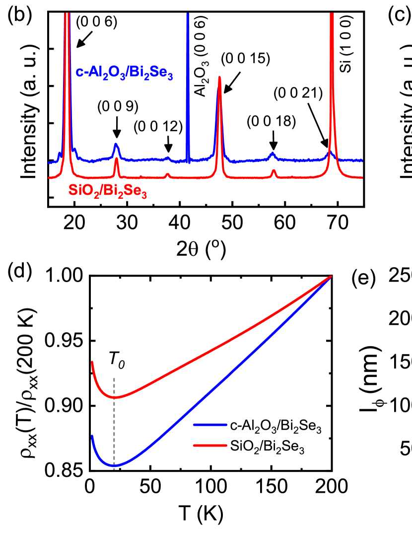
The formation of Bi2Se3 phase in our films is confirmed by Raman study which shows the normal modes (figure 1(c)) corresponding to the vibrations parallel ( and ) and normal () to c-axis [46] of Bi2Se3 crystal. Sharp vertical streaks in RHEED pattern (figure 1(a), left) of Bi2Se3 films on c-Al2O3 imply atomically flat 2D surface with small domains. For Bi2Se3 films on SiO2 substrate, streaks in RHEED pattern with modulated intensity (figure 1(a), right) suggests flat surface with small multilevel steps. XRD analysis, using Cu source, shows (0 0 3) family of planes (figure 1(b)) suggesting c-axis oriented growth of Bi2Se3 even on SiO2 substrate [47]. In the case of SiO2 substrate, in-plane amorphous growth is expected which was noted using isotropic RHEED pattern with in-plane sample rotation [44]. Despite the above growth conditions in SiO2/Bi2Se3 films, studies in literature have demonstrated the presence of robust Dirac surface states [44, 48].
Hall measurement of the films grown on the two substrates reveal an electron carrier concentration, cm-2 and mobility, in the range of cm2/Vs. For all the batch of samples, comparatively, c-Al2O3/Bi2Se3 films show a higher than the SiO2/Bi2Se3 films. While cooling down, both the films show a metallic signature with an upturn in resistivity at lower temperatures (figure 1(d)). Here, SiO2/Bi2Se3 films show relatively gradual decrease in the resistivity suggesting the presence of higher bulk disorder in comparison to the films on c-Al2O3. However, in both the samples, the upturn in resistance appears at almost the same temperature K indicating that the underlying mechanism to the upturn is independent of choice of substrate. We discuss this in detail in the following section.
III.2 Evidence of EEI and background correction
The observed resistivity upturn in figure 1(d) could originate from different mechanisms such as disorder [49, 50], WL [51] and EEI [36]. In highly disordered metal, an insulating transition emerge if the mean free path of the electrons () becomes smaller than the Fermi wavelength (). Based on the above argument, Ioffe and Regel derived [52] a critical limit for the mobility, ( is the thickness of the film), below which a disorder driven insulating transition can be observed. Mobility in our 16 nm Bi2Se3 films (obtained from Hall measurements) is found to be much above the critical limit ( cm2/Vs, see section 1 in supplementary information for more details), allowing us to rule out the strong upturn response in resistivity due to film disorder effects. Additionally, the observation of similar resistivity upturn at K in both the samples also confirm these findings.
In a weakly disordered system where is larger than , EEI accompanied by the impurity scattering can result in a reduction of electron density of states near Fermi level () [53]. For 3D, the temperature dependency due to EEI shows [36]. However, the effect becomes two dimensional (2D) when thermal diffusion length (, is the diffusion constant) becomes larger than the film thickness and gives a dependency [36] as follows,
| (2) |
here, is Coulomb screening factor and is the characteristic temperature for EEI effect. We have measured nm in 16 nm Bi2Se3 films which suggest the 2D nature of the EEI in our samples.
Beside the effect of EEI, in a system with strong spin-orbit interaction, the quantum interference (QI) effects i,e WAL or WL behaviour of the charge carriers also produces an increase or decrease in conductivity with decreasing temperature [51],
| (3) |
where and , respectively for WL and WAL effect. is the characteristic temperature for the QI effects. can be defined by the dependency of phase coherence length, and it depends on the dimentionality and type of dephasing mechanism present in the system [54]. For EEI in an effectively 2D system, .
To understand the type of interaction responsible for the dephasing mechanism in our system, we have measured as a function of from the MC measurements with OOP magnetic field at different temperatures. is determined from the fitting of Hikami-Larkin-Nagaoka equation [51],
| (4) |
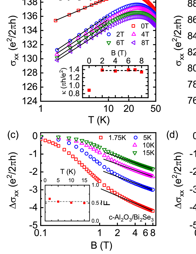
to the OOP WAL signal (shown in supplementary figure 2(a) and 2b). Here is the digamma function and the dephasing field . gives the effective number of 2D channels contributing to the WAL effect. Ideally, in 3D TI films, the presence of two TSSs (top and bottom) should give . But, in case of Bi2Se3, lies inside the bulk conduction band (CB) due to high concentration of Se vacancies and the conducting bulk states weakly couple the top and bottom TSSs [55, 11, 56] making smaller than 2. From the fitting of equation (4), measured value of up to K, is observed to be nearly independent of temperature (shown in supplementary figure 2(c)) with average value and for c-Al2O3/Bi2Se3 and SiO2/Bi2Se3 films, respectively. In figure 1(e) we plot vs and the fitting shows for both type of films confirming the presence of EEI in our system.
Since, in our Bi2Se3 films, WAL behaviour (confirmed by MC study) and EEI (confirmed by measured ) coexists, both of them contribute to the behaviour of as given by equation (2) and equation (3). At , the overall slope (equation (1)) can be written as . Here, the contribution of WAL or WL effect to the temperature dependence of can be suppressed by applying high magnetic fields [34, 36] and the value of the screening factor can be determined by measuring . In figure 2(a) & 2(b), the logarithmic nature of with is shown for different magnitude of OOP magnetic fields. The inset shows the value of for different . For sufficiently large value of (), saturates suggesting the complete suppression of WAL nature of charge carriers. The difference is ve i,e the effective which implies, WAL is a dominant mechanism in our films for small magnetic fields and the surface electrons are the majority charge carriers [31, 30]. However, in the above analysis, we have observed two discrepancies: (i) our measurement shows at large i,e ; this requires which is not physical as by definition, and (ii) from vs plot, we have measured and for c-Al2O3/Bi2Se3 and SiO2/Bi2Se3 films, respectively. provides the values of for both type of the films (), which deviates from the measured ( and for films on c-Al2O3 and SiO2, respectively) from HLN fitting of measured MC.
Similar discrepancy in the value of was observed in Cu doped Bi2Se3 films [41] and Bi2Te3 films [42] and attributed to strong spin orbit coupling (SOC) present in the TIs. Recent theoretical study [31] suggests that these discrepancies arise due to the presence of band-edge bulk channels which contribute to the WL effect beside the WAL effect from the TSSs. In the section II.C we have analysed low field MC considering the WAL effect from the surface states and WL effect from the band-edge bulk states and show that this is indeed the case in our Bi2Se3 samples.
Since in our samples the value of cannot be obtained by measuring , we have taken a different approach [33]. In the 2D limit, by neglecting SOC effects, the correction to MC () due to EEI can be written as [36],
| (5a) | |||
| (5b) | |||
here . The above equation is found to provide a decent approximation of EEIs in TIs [35, 33, 34]. At high magnetic fields when Zeeman energy is much larger than the thermal activation energy (), ) and , arising from EEI, shows a linear behaviour with . At K, this limit requires kOe. In our MC measurements, this linear response is observed (figure 2(c) & 2(d)) for T (along the film plane). At this high in-plane magnetic field, WAL signal from the TSSs can be neglected and from the linear fit (solid black line in figure 2(c) & 2(d)) the effective value of is estimated [33] to be and for films on c-Al2O3 and SiO2, respectively.
As shown in equation (5), we need the value of to estimate the contribution of EEI in . Kohler and Wuchner have estimated the value of conduction electrons’ -factor to be and respectively for magnetic field’s direction parallel and perpendicular to c-axis of Bi2Se3 crystal using Shubnikov-de Haas oscillation measurements [38]. Recently, more precise electron spin resonance (ESR) measurements by Wolos et al. have shown the value of -factor for conduction electron to be equal to and for magnetic field parallel and perpendicular to c-axis [37]. In the following analysis, the extracted value of and -factor values, from ESR measurements, are used to determining the field dependence of (equation (5)) and subsequently the EEI background correction to the measured MC is performed.
III.3 OOP and IP MC studies
Studies by H. T. He et al. [13] suggest the existence of magnetoresistance proportional to due to Lorentz deflection of bulk charge carriers. The corresponding correction to the MC can be written as, , where according to Kohler’s rule [13, 58] , is the film mobility. However, due to relatively low of our films this contribution is very small as compared to the measured MC (see supplementary figure 3(a)) and therefore is neglected in our MC analysis.
In a Dirac system like topological insulators, the Berry phase acquired by the electrons after completing a closed loop on the Fermi surface, can be written as [18, 59]. Here, is the Dirac mass and is the Fermi level referenced from the Dirac point. For the surface states, , and the corresponding leads to a destructive quantum interference and thus the TSSs shows WAL effect. On the other hand, the bulk states have a finite gap and when is near the conduction band-edge . In this situation, electrons in the gaped band-edge bulk states, goes through a constructive interference upon tracing a closed path, leading to WL effect. Therefore, the experimentally observed WAL in TIs could be a combined result of WL from band-edge bulk states and WAL from surface states [30, 31].
In our Bi2Se3 films the Hall carrier density is cm-2 which places the near the bottom of the bulk conduction band [60, 48]. However, capping the Bi2Se3 films with thick Se layer can reduce the top surface carrier concentration [48] significantly and can bring the surface closer to the Dirac point. This mismatch between the surface and bulk can further lead to a upward band bending near the top surface and can bring the bulk Fermi level closer to the conduction band-edge [50, 26] making for band-edge bulk states. Therefore, in our Bi2Se3 thin films, band-edge WL channel and surface WAL channels may coexist. The corresponding quantum correction formula for the MC in presence of OOP magnetic field can be written as [30],
| (6) |
where, corresponds to the (WL) and corresponds to (WAL) situation. . In the limit and , represents the phase coherence length [30, 31]. To replicate more realistic scenario, we are assuming that the phase coherence length for surface states and band-edge bulk states are different i,e . Theoretically and (top and bottom 2D surface channel). In our analysis, we keep as a fitting parameter as the top and bottom surface states can be weakly coupled through the conducting bulk [55, 11, 56].
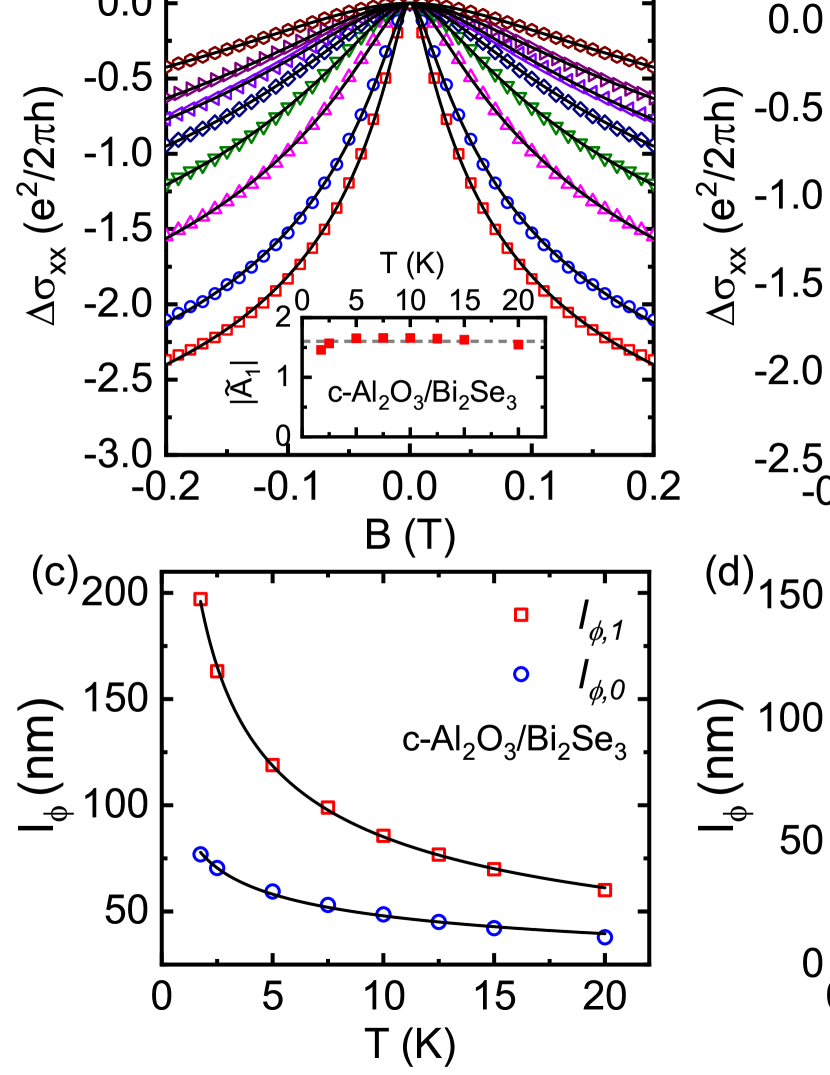
As mentioned in the previous section, the contribution of EEI needs to be removed from the MC data for accurate analysis. In figure 3(a) & 3(b), we have shown the measured OOP MC of both films after the subtraction of EEI contributions. The fitting with equation 6 is shown by solid lines. Corresponding value of (shown in the inset) is observed to be almost independent of temperature. Dashed gray line shows the average value. The measured value of and is plotted with respect to (figure 3(c) & 3(d)) and fitted with . We measure (corresponds to TSSs) for both types of films which agrees with the theoretically expected in case of 2D EEI. For the electrons in band-edge bulk states, we measure and for c-Al2O3/Bi2Se3 and SiO2/Bi2Se3 films respectively, which is smaller than the theoretical value. However, similar value of has been observed before in Bi2Se3 micro flakes [chiu2013weak] and few-layer WTe2 [zhang2020crossover] in presence of EEI. The smaller value of may suggest the presence of other weak dephasing effects [huang2007observation, 54] within the bulk which is beyond the scope of present work.
Our analysis shows for SiO2/Bi2Se3 films which is higher than measured for c-Al2O3/Bi2Se3 films. This suggests comparably weaker coupling between top and bottom TSS in SiO2/Bi2Se3 films. The phase coherence length of the TSSs () is relatively bigger ( bigger at 1.75 K) in c-Al2O3/Bi2Se3 films whereas is marginally higher in these films. gives a measure of disorder present in the system and it gets smaller with increasing disorder [60]. Comparably smaller value of in SiO2/Bi2Se3 films may suggest the presence of higher disorder in these films which is also observed in the RHEED images and the value of obtained from the Hall measurements. The presence of disorder can effectively decouple the top and bottom surface states [60, 29] resulting in a higher value of as observed in our SiO2/Bi2Se3 samples. Previous reports have achieved similar decoupling between the top and bottom TSSs in TI thin films by tuning the Fermi level [20, 60], modulating the film thickness [49] and controlling the disorder by varying the annealing conditions [29].
From the extracted values of and we obtain to be equal to 0.488 and 0.541 for c-Al2O3/Bi2Se3 and SiO2/Bi2Se3 films, respectively ( corresponds to fitting of ). These values are in very good agreement with the values measured from the vs plot confirming the existence of two types of conducting channel in our samples. The presence of two types of conducting channels can also explain the measured [31] in section III.2. When multiple transport channels exist, for can be written as [61], , where runs over independent WL and WAL channels, is a scaling factor and is the Coulomb screening factor. has the values and for and 1, respectively. In comparison to the previous approach in Section III.2 to determine the overall value of using equation (5), the present expression of includes weighted values of for the two independent transport channels.
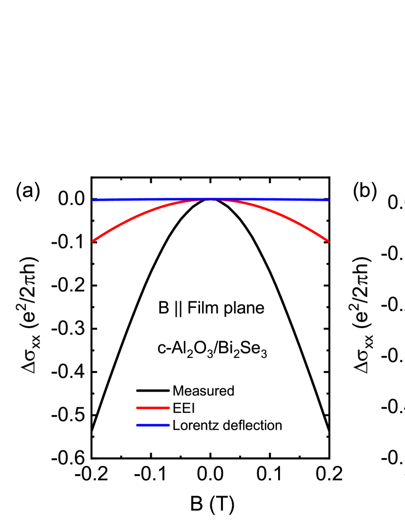
Beside the usual OOP WAL response, we have also observed a strong WAL signal when field is applied parallel to Bi2Se3 film (solid black line in figure 4(a)). A -ve MC in IP magnetic field can arise from the Lorentz deflection of charge carriers in the bulk of the TI [13]. EEI can also contribute to the IP MC as described in the previous section. Estimated value of these two effects is compared with the observed IP WAL signal in figure 4(a).
At low fields, the contribution from Lorentz deflection (4(a), solid blue line) is negligible as compared to the observed signal due to small of our Bi2Se3 samples. Estimated correction to the MC from EEI effect is also much smaller than the measured value (4(a), solid red line). This suggests the presence of nontrivial effects which contribute to strong IP WAL signal in our Bi2Se3 samples. Recent theoretical developments shows that TIs can exhibit IP MC due to the exponential decay of TSSs wavefunction into the bulk [27] which effectively results in a finite thickness of the 2D-TSSs. First principle studies of Bi2Se3 system [62] have estimated the penetration depth of the TSSs to be up to 2-3 quintuple layers (1 quintuple layer 0.955 nm [46]). When magnetic field is applied along the film plane, magnetic flux through the finite cross-section of the TSSs (figure 4(e)) can give rise to a -ve MC. Corresponding correction to the MC is derived by Tkachov and Hankiewicz [27](TH) model,
| (7) |
where, and is the penetration depth. For perfectly two dimensional TSS (i,e ) this correction vanishes.
figure 4(b) & 4(c) shows the measured value of IP WAL signal at different temperatures after removing the EEI background. Correction due to Lorentz deflection of charge carriers has been neglected due to its negligible magnitude. Solid black lines represent the best fit using equation (7) with as the fitting parameter. The measured value of from figure 3 is used in the fitting to consider the weak coupling between top and bottom surface states. The range of magnetic field used in the fitting is much greater than the dephasing field of the TSSs. Measured from the fitting of equation (6) (as shown in figure 3(a) & 3(b)) has been used to compute the value of using the TH model fitting. Our analysis shows similar value of for the two types of films with nm at 1.75 K. Our Bi2Se3 samples show much smaller value of as compared to the recently reported nm on 50 nm thick Te doped Bi2Se3 films [28] that also introduces considerable structural disorder. H Park et al. measured nm for a 14 nm thick doped Bi2Se3 films. The measured in our samples is higher than the previously estimated values from first principle calculations [62]. The reason behind large could be the phase coherent trajectories of surface charge carriers through the conducting bulk [21], in a perpendicular direction to the film plane, coupling the top and bottom surface states weakly (as shown schematically in figure 4(e)). However, we measure for all the temperatures suggesting a better decoupling between the TSSs which also supports the observation of close to the value 2. Interestingly, SiO2/Bi2Se3 samples have a similar penetration depth and stronger decoupling (larger ) between the two TSSs as compared to c-Al2O3/Bi2Se3 films.
III.4 AMC study
Since our observations show the effect of TSSs on the MC for both IP and OOP magnetic field originating from two distinct mechanisms, we now try to probe their combined response on the AMC of Bi2Se3 films. Recently, Hui Li et al. [63] studied the AMC of BiSbTeSe2 thin films, but in their analysis, the WAL contribution of the 2D surface states at IP magnetic field has been neglected. In contrast, our study has shown a considerable IP WAL signal arising from the finite penetration depth of the surface states.
At low temperatures where the effects of TSSs is dominant (for both IP and OOP configuration), we write an expression for the AMC by only considering the WAL behaviour for IP (equation (7)) and OOP (equation (6)) magnetic field,
| (8) |
Here, is the value of the conductance when no magnetic field is applied. 2nd term describes the correction arising from the bulk band-edge WL channels due to the OOP component of the magnetic field. 3rd term represents the WAL effect from TSSs for IP and OOP component of . is the angle between and the film-normal (see figure 5(b)).
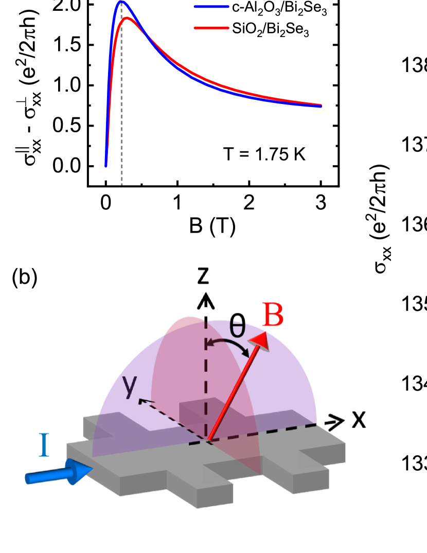
For our devices, the difference of IP and OOP MC is maximum around T (figure 5(a)). Keeping this fact into consideration, we have chosen to measure the anisotropy in MC with T. The rotation schemes of the measurements is shown in figure 5(b). Magnetic field is rotated in x-z plane and y-z plane. Our measurements show a highly anisotropic nature of MC with a sharp peak at . We have observed no significant difference in the AMC for the rotation of in the x-z and y-z plane (see supplementary figure 4) which suggest the absence of IP anisotropy in the MC of our Bi2Se3 films.
An OOP anisotropy in can appear from EEI background due to the anisotropy in the value of -factor of Bi2Se3 [37]. For this purpose, the -factor in equation (5) is replaced with , where and are the -factor value of conduction electrons for OOP (parallel to c-axis) and IP (perpendicular to c-axis) magnetic field, respectively. The additional anisotropy in EEI due to high SOC [64, 65] is expected to be weak in our AMC study as these measurements were performed at low magnetic fields.
The measured AMC at different temperatures, after the EEI background correction using equation (5), is shown in figure 5(c) & 5(d). The observed AMC is well fitted with equation (8) (solid black lines in figure 5(c) & 5(d)). To reduce the number of fitting parameters and to keep the analysis simple, we have kept the WL correction fixed by keeping and fixed at the values, obtained in Section III.3 from WAL analysis. The parameters , and in equation (8) are used as the fitting parameters in the analysis and is measured experimentally.
The observed sharp peak in the AMC near at low temperatures arises due to the WAL effect in TSSs for OOP component of the magnetic field. The WAL signal due to the finite thickness of TSSs for IP component of gives a correction to the peak height at . Fitting results of equation (8) shown in figure 5(e)-5(g) yields similar value of , and to those, measured independently from OOP and IP WAL analysis, earlier in the section III.3. At 1.75 K, AMC study gives nm and nm for c-Al2O3/Bi2Se3 and SiO2/Bi2Se3 films respectively which are smaller than the values ( nm and nm, respectively) obtained from WAL study in section III.3. However, this mismatch in reduces with increasing temperature. Extracted value of from the fitting of equation (8) matches reasonably with the values measured from WAL study. Although the values of obtained from AMC study (figure 5g) and IP WAL study (figure 4d) match near lowest temperatures, it deviates considerably at higher temperatures showing almost half of the value obtained from IP WAL studies. This mismatch is possibly arising because the IP-WAL signal becomes significantly weaker at higher (See figure 4(b) & 4(c)), possibly making the anisotropy in the magnetoconductance of the bulk Bi2Se3 comparable which has been neglected in our analysis. Nevertheless, equation (8) provides a good estimate of , and which are extracted simultaneously and explains the AMC data reasonably well. Our above observations indicate that the investigated AMC analysis can serve as a useful technique to probe the TSSs in 3D TIs.
IV Conclusion
In conclusion, our study of Bi2Se3 thin films show that EEIs give a considerable contribution to the total MC. We provide details of a systematic approach to remove these contributions for the analysis of WAL (for both IP and OOP configuration) and AMC. We show that the discrepancy in the and dependence of can be resolved by considering WL effects from the band-edge bulk states. For IP magnetic fields, a strong WAL signal with nontrivial origin is observed that finds applicability of the TH model to explain our IP MC study. Additionally, we also convey the significance of finite penetration depth of TSSs in analyzing the AMC experiments. The fitting routine using a combination of HLN model and TH model explains the AMC in our Bi2Se3 films and the fitting parameters, which characterise the TSSs, show the expected trend. Importantly, we find that Bi2Se3 films on SiO2 with stronger bulk-disorder than on c-Al2O3 can lead to a better decoupling of the two TSSs.
V Acknowledgement
Authors thank Dr. T. N. Narayanan for providing access to Raman facility. We are also grateful to IIT Hyderabad for giving access to their XRD facility. Authors acknowledge funding support of the Department of Atomic Energy, Government of India, under Project Identification No. RTI 4007 and Science and Engineering Research Board Grant No. CRG/2019/003810.
Data Availability
Data that support the findings of this study is available from the corresponding authors upon reasonable request.
References
- [1] Fu L, Kane C L and Mele E J 2007 Phys. Rev. Lett. 98 106803
- [2] Hasan M Z and Kane C L 2010 Rev. Mod. Phys. 82 3045–3067
- [3] Zhang H, Liu C X, Qi X L, Dai X, Fang Z and Zhang S C 2009 Nat. Phys. 5 438–442
- [4] Moore J E 2010 Nature 464 194–198
- [5] Qi X L and Zhang S C 2011 Rev. Mod. Phys. 83 1057–1110
- [6] Ando T, Nakanishi T and Saito R 1998 J. Phys. Soc. Japan 67 2857–2862
- [7] Suzuura H and Ando T 2002 Phys. Rev. Lett. 89 266603
- [8] Kong D and Cui Y 2011 Nat. Chem. 3 845–849
- [9] He M, Sun H and He Q L 2019 Front Phys 14 43401
- [10] Checkelsky J G, Hor Y S, Liu M H, Qu D X, Cava R J and Ong N 2009 Phys. Rev. Lett. 103 246601
- [11] Chen J, Qin H, Yang F, Liu J, Guan T, Qu F, Zhang G, Shi J, Xie X, Yang C et al. 2010 Phys. Rev. Lett. 105 176602
- [12] Checkelsky J G, Hor Y S, Cava R J and Ong N 2011 Phys. Rev. Lett. 106 196801
- [13] He H T et al. 2011 Phys. Rev. Lett. 106 166805
- [14] Liu M, Zhang J, Chang C Z, Zhang Z, Feng X, Li K, He K, Wang L l, Chen X, Dai X et al. 2012 Phys. Rev. Lett. 108 036805
- [15] Zhang D, Richardella A, Rench D W, Xu S Y, Kandala A, Flanagan T C, Beidenkopf H, Yeats A L, Buckley B B, Klimov P V et al. 2012 Phys. Rev. B 86 205127
- [16] Yang Q I et al. 2013 Phys. Rev. B 88 081407
- [17] Lang M, He L, Kou X, Upadhyaya P, Fan Y, Chu H, Jiang Y, Bardarson J H, Jiang W, Choi E S et al. 2013 Nano Lett. 13 48–53
- [18] Lu H Z, Shi J and Shen S Q 2011 Phys. Rev. Lett. 107 076801
- [19] Lu H Z, Shan W Y, Yao W, Niu Q and Shen S Q 2010 Phys. Rev. B 81 115407
- [20] Steinberg H, Laloë J B, Fatemi V, Moodera J S and Jarillo-Herrero P 2011 Phys. Rev. B 84 233101
- [21] Lin C, He X, Liao J, Wang X, Sacksteder IV V, Yang W, Guan T, Zhang Q, Gu L, Zhang G et al. 2013 Phys. Rev. B 88 041307
- [22] Shan W Y, Lu H Z and Shen S Q 2010 New J. Phys. 12 043048
- [23] Zhang Y, He K, Chang C Z, Song C L, Wang L L, Chen X, Jia J F, Fang Z, Dai X, Shan W Y et al. 2010 Nat. Phys. 6 584–588
- [24] Li M, Song Q, Zhao W, Garlow J A, Liu T H, Wu L, Zhu Y, Moodera J S, Chan M H, Chen G et al. 2017 Phys. Rev. B 96 201301
- [25] Eremeev S V et al. 2013 Phys. Rev. B 88 144430
- [26] Mathimalar S, Sasmal S, Bhardwaj A, Abhaya S, Pothala R, Chaudhary S, Satpati B and Raman K V 2020 npj Quantum Mater. 5 1–6
- [27] Tkachov G and Hankiewicz E 2011 Phys. Rev. B 84 035444
- [28] Stephen G M, Vail O A, Lu J, Beck W A, Taylor P J and Friedman A L 2020 Sci. Rep. 10 1–7
- [29] Park H, Chae J, Jeong K, Choi H, Jeong J, Kim D and Cho M H 2018 Phys. Rev. B 98 045411
- [30] Lu H Z and Shen S Q 2011 Phys. Rev. B 84 125138
- [31] Lu H Z and Shen S Q 2014 Phys. Rev. Lett. 112 146601
- [32] Zhang H, Yu H, Bao D, Li S, Wang C and Yang G 2012 Phys. Rev. B 86 075102
- [33] Liu M, Chang C Z, Zhang Z, Zhang Y, Ruan W, He K, Wang L l, Chen X, Jia J F, Zhang S C et al. 2011 Phys. Rev. B 83 165440
- [34] Chen J, He X, Wu K, Ji Z, Lu L, Shi J, Smet J and Li Y 2011 Phys. Rev. B 83 241304
- [35] Wang J et al. 2011 Phys. Rev. B 83 245438
- [36] Lee P A and Ramakrishnan T 1985 Rev. Mod. Phys. 57 287
- [37] Wolos A, Szyszko S, Drabinska A, Kaminska M, Strzelecka S, Hruban A, Materna A, Piersa M, Borysiuk J, Sobczak K et al. 2016 Phys. Rev. B 93 155114
- [38] Köhler H and Wöchner E 1975 Phys Status Solidi B 67 665–675
- [39] Analytis J G, McDonald R D, Riggs S C, Chu J H, Boebinger G and Fisher I R 2010 Nat. Phys. 6 960–964
- [40] Taskin A and Ando Y 2011 Phys. Rev. B 84 035301
- [41] Takagaki Y, Jenichen B, Jahn U, Ramsteiner M and Friedland K J 2012 Phys. Rev. B 85 115314
- [42] Roy A, Guchhait S, Sonde S, Dey R, Pramanik T, Rai A, Movva H C, Colombo L and Banerjee S K 2013 Appl. Phys. Lett. 102 163118
- [43] Bansal N, Kim Y S, Edrey E, Brahlek M, Horibe Y, Iida K, Tanimura M, Li G H, Feng T, Lee H D et al. 2011 Thin Solid Films 520 224–229
- [44] Bansal N et al. 2014 Appl. Phys. Lett. 104 241606
- [45] Chen Z, Garcia T A, De Jesus J, Zhao L, Deng H, Secor J, Begliarbekov M, Krusin-Elbaum L and Tamargo M C 2014 J. Electron. Mater. 43 909–913
- [46] Zhang J, Peng Z, Soni A, Zhao Y, Xiong Y, Peng B, Wang J, Dresselhaus M S and Xiong Q 2011 Nano Lett. 11 2407–2414
- [47] Jerng S K, Joo K, Kim Y, Yoon S M, Lee J H, Kim M, Kim J S, Yoon E, Chun S H and Kim Y S 2013 Nanoscale 5 10618–10622
- [48] Liu Y, Chong C, Jheng J, Huang S, Huang J, Li Z, Qiu H, Huang S and Marchenkov V 2015 Appl. Phys. Lett. 107 012106
- [49] Brahlek M, Koirala N, Salehi M, Bansal N and Oh S 2014 Phys. Rev. Lett. 113 026801
- [50] Brahlek M, Koirala N, Bansal N and Oh S 2015 Solid State Comm. 215 54–62
- [51] Hikami S, Larkin A I and Nagaoka Y 1980 Prog. Theor. Phys. 63 707–710
- [52] Ioffe A and Regel A 1960 Prog. Semicond. 4 237
- [53] Altshuler B and Aronov A 1979 Solid State Commun 30 115–117
- [54] Lin J J and Bird J 2002 J. Phys. Condens. Matter 14 R501
- [55] Bansal N, Kim Y S, Brahlek M, Edrey E and Oh S 2012 Phys. Rev. Lett. 109 116804
- [56] Kim Y S, Brahlek M, Bansal N, Edrey E, Kapilevich G A, Iida K, Tanimura M, Horibe Y, Cheong S W and Oh S 2011 Phys. Rev. B 84 073109
- [57] Mathur H and Baranger H U 2001 Phys. Rev. B 64 235325
- [58] Olsen J L 1962 Interscience Publishers, New York
- [59] Ghaemi P, Mong R S and Moore J E 2010 Phys. Rev. Lett. 105 166603
- [60] Kim D, Syers P, Butch N P, Paglione J and Fuhrer M S 2013 Nat. Commun. 4 2040
- [61] Tkáč V, Vỳbornỳ K, Komanickỳ V, Warmuth J, Michiardi M, Ngankeu A, Vondráček M, Tarasenko R, Vališka M, Stetsovych V et al. 2019 Physical review letters 123 036406
- [62] Zhang W, Yu R, Zhang H J, Dai X and Fang Z 2010 New J. Phys. 12 065013
- [63] Li H, Wang H W, Li Y, Zhang H, Zhang S, Pan X C, Jia B, Song F and Wang J 2019 Nano Lett. 19 2450–2455
- [64] Fukuyama H 1982 J. Phys. Soc. Japan 51 1105–1110
- [65] Markiewicz R and Rollins C 1984 Phys. Rev. B 29 735