Vertical Strain-Induced Modification of the Electrical and Spin Properties of Monolayer MoSi2X4 (X= N, P, As and Sb)
–ٰ
Abstract
In this work, the electrical and spin properties of monolayer MoSi2X4 (X= N, P, As, and Sb) under vertical strain are investigated. The band structures state that MoSi2N4 is an indirect semiconductor, whereas other compounds are direct semiconductors. The vertical strain has been selected to modify the electrical properties. The bandgap shows a maximum and decreases for both tensile and compressive strains. The valence band at K-point displays a large spin-splitting, whereas the conduction band has a negligible splitting. On the other hand, the second conduction band has a large spin-splitting and moves down under vertical strain which leads to a large spin-splitting in both conduction and valence bands edges. The projected density of states along with the projected band structure clarifies the origin of these large spin-splittings. These three spin-splittings can be controlled by vertical strain.
I Introduction
The graphene, the first member of two-dimensional (2D) materials, with honeycomb structure does not exhibit an electronic band gap Neto et al. (2009). This problem has motivated the researchers to explore and design novel two-dimensional semiconductors, such as the transition metal dichalcogenides Radisavljevic et al. (2011), black phosphorene Guan et al. (2014), antimonene Zhang et al. (2015) and indium selenideMudd et al. (2013). Therefore, exploring new 2D materials with proper electronic properties for particular applications is highly demanded. After monolayer TMDC, 2D transition metal nitride (TMN) have been proposed in the recent years Li et al. (2017); Wang et al. (2016); Ozdemir (2018). Since TMNs do not contain layered structures, the fabrication of large-area TMNs monolayers has remained challenging. Recently, MoSi2N4 monolayer based on TMN and without 3D counterpart structure has been synthesizedHong et al. (2020). MoSi2N4 is constructed from a MoN2 monolayer sandwiched between two Si-N monolayers. By analyzing MoSi2N4 monolayer, it can be realized that with sandwiching a TMDC-type MZ2 monolayer into InSe-type A2Z2, twelve different structures with MA2Z4 formula have been achieved. They demonstrate different phases such as semiconductor, topological insulators, and Ising superconductors Wang et al. (2021). Monolayer MoSi2N4 has been successfully fabricated using chemical vapor deposition with large size of up to 15mm15mmHong et al. (2020). This compound demonstrates high strength and excellent stability at ambient. MoSi2N4 compound also shows an elastic constant three times larger than monolayer MoS2. In addition, the large electron and hole mobility is estimated to be 270/1200 cm2/Vs that is four to six times higher than MoS2 ones. This high mobility along with outstanding stability in the ambient environment makes this material a promising candidate for future applications. Other members of MoSi2N4 family with MA2Z4 formula (M = Transition metal, A = Si, Ge and Z = N, P, As) have been extensively investigated Zhong et al. (2021); Wang et al. (2021). These monolayers exhibit a wide range from semiconducting to metallic properties. In addition, some compounds with magnetic transition metal elements also represent magnetic propertiesLi et al. (2021). The MoSi2N4 and WSi2N4 monolayers also show high lattice thermal conductivity for thermoelectric applications Mortazavi et al. (2021); Yu et al. (2021). Monolayer MoSi2N4 and its family also have suitable band gaps up to 1.73eV for potential optical applications in the visible rangeBafekry et al. (2021a); Yao et al. (2021). It has been anticipated that MoSi2N4 family compounds have a pair of valley pseudospins similar to monolayer MoS2 Yang et al. (2021). These monolayers have been also predicted to exceed monolayer MoS2 due to fascinating valleytronic properties, for instance, multiple-folded valleys in monolayer MoSi2As4. The lack of inversion symmetry along with strong spin-orbit coupling from transition metal elements in the MA2Z4 family results in two inequivalent valleys (K and K’) with sizable spin-splitting and spin-valley coupling Ai et al. (2021). For example, WSi2N4 demonstrates a large spin-splitting at both conduction and valence bands at K and K’-valleys together with spin-valley coupling. It has been confirmed theoretically and experimentally that a semiconductor to metal transition occurs in multi-layer MoS2 by applying vertical strain Nayak et al. (2014); Chi et al. (2014); Ghobadi (2019). Totally, the decrease of interlayer distance may lead to charge redistribution and semiconductor to metal transition. The out-of-plane strain is presented as a powerful tool to tune the electrical properties of bilayer MA2Z4 family Bafekry et al. (2021b). For instance, the bandgap of bilayer MoSi2N4 decreases with increasing compressive strain and the bandgap closes at the strain of 22. Such a semiconductor to metal transition also occurs in other MA2Z4 bilayers Zhong et al. (2021). The transition pressure is distributed from 2.18 GPa in CrSi2N4 to 32.04 GPa in TiSi2N4. In another work, the biaxial strain is used to tune the band gaps of bilayer MoSi2N4 and WSi2N4 Wu et al. (2021). It has been reported that these compounds demonstrate a direct bandgap at compressive strain. Furthermore, it has been shown that strain can also modify the electronic and magnetic properties of VSi2P4 monolayer Guo et al. (2020). The strain increasing changes the phase of this monolayer from a ferromagnetic metal to a spin-gapless semiconductor, afterward to a ferromagnetic semiconductor, and then come back to spin-gapless semiconductor and finally to a ferromagnetic half-metal. In this work, the effects of vertical strain on the electrical and spin properties of monolayer MoSi2X4 (X=N, P, As, and Sb) are investigated. First, the electrical properties such as bandgap, effective mass, and band edge locations are obtained at equilibrium. In the following, vertical strain is applied to all materials, and the variation of band gaps, band edges, and charge densities are explored. Finally, spin-splitting at both equilibrium and strained samples is studied.
II Computational details
In order to investigate the electrical and spin properties of MoSi2X4 (X= N, P, As and Sb) monolayers, density functional calculations are performed using the SIESTA package Soler et al. (2002). The generalized gradient approximation (GGA) with the Perdew-Burke-Ernzerhof (PBE) Perdew and Zunger (1981) functional is employed for the exchange-correlation term. We have adopted fully relativistic pseudopotentials and have taken into account the effect of spin-orbit coupling (SOC). A Monkhorst-Pack k-point grid of is chosen for the unit-cell. The energy cutoff is set to be 200 Ry and a double- plus polarization basis-set is used. The total energy is converged to better than eV and the geometries are fully relaxed until the force on each atom is less than 0.02 eV/. A vacuum region of 30 is added to avoid interactions in the normal direction. To visualize the atomic structures, XCrySDen package has been used Kokalj (2003). The out-of-plane strain is defined as , where and are the equilibrium and deformed compound thickness, respectively. The effective masses are calculated by using the following equation Touski and Ghobadi (2020); Ghobadi and Touski (2020),
| (1) |
Here, is the reduced Planck constant, E and k are the energy and wave vector of conduction band minimum and valence band maximum.
| a() | dMo-X() | dSi-X() | () | Thickness() | C11(N/m) | C12(N/m) | |
|---|---|---|---|---|---|---|---|
| MoSi2N4 | 2.928 | 2.111 | 1.763 | 0.531 | 7.119 | 472.66 | 142.02 |
| MoSi2P4 | 3.486 | 2.477 | 2.253 | 1.046 | 9.486 | 207.77 | 58.46 |
| MoSi2As4 | 3.633 | 2.583 | 2.366 | 1.136 | 10.021 | 178.03 | 54.75 |
| MoSi2Sb4 | 3.898 | 2.777 | 2.589 | 1.278 | 10.991 | 141.40 | 47.72 |
III Results and discussion
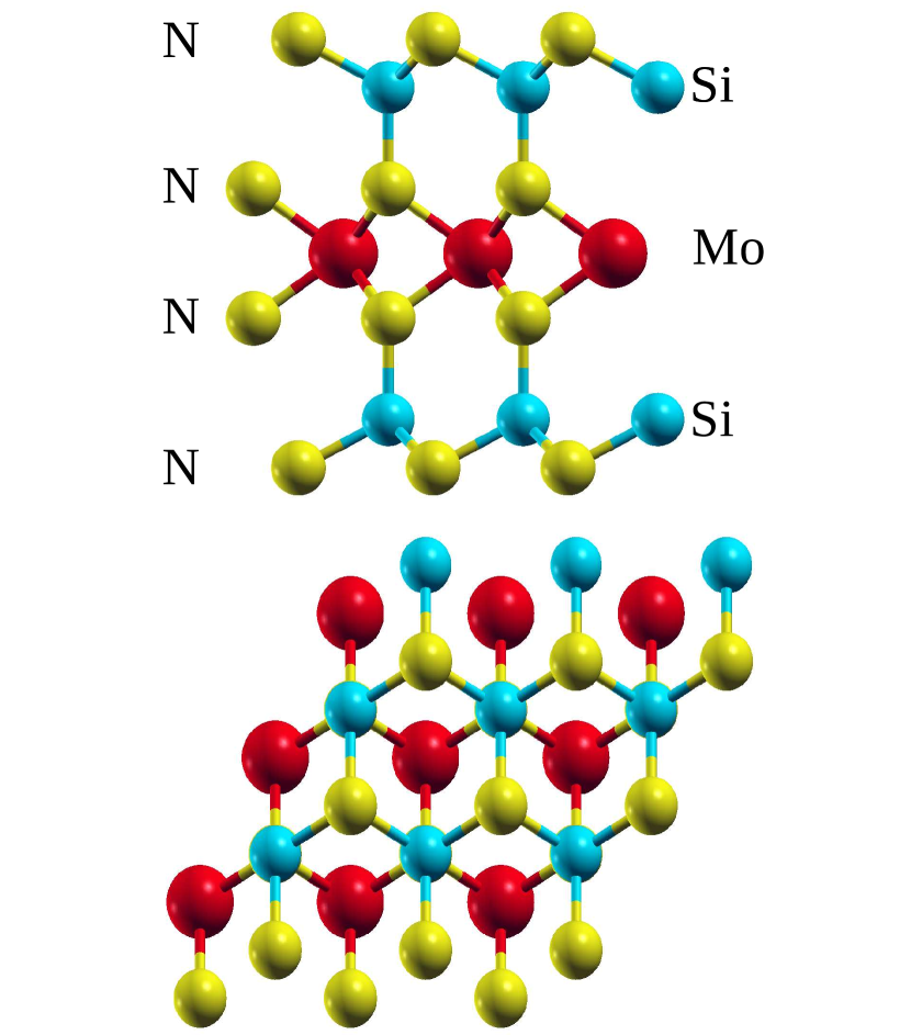
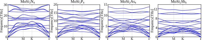
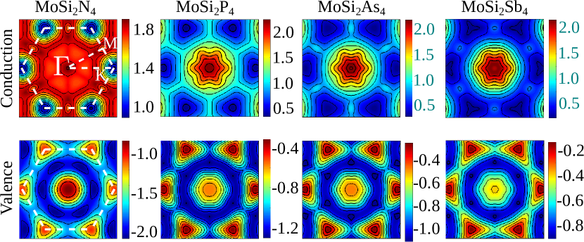
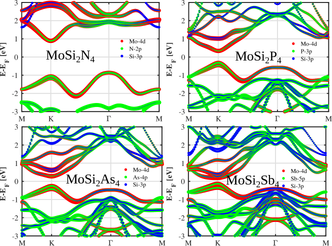
The schematic of the studied compounds is shown in Fig. 1. As it is obvious, a MoN2 monolayer is sandwiched between two SiN monolayers. The unsaturated Si atoms in SiN sub-layer bond with unsaturated N atoms in MoN2. The structural and mechanical properties of four monolayers are presented in Table 1. The lattice constant of MoSi2N4 is 2.928 that is close to experimental resultHong et al. (2020). The lattice constants of MoSi2P4 and MoSi2As4 are also 3.486 and 3.633 , respectively, that are compatible with previous studies Guo et al. (2020); Ai et al. (2021). The lattice constant increases for the compounds with heavier X elements. This behavior can be observed in the Mo-X bond length () in MoX2 sub-layer, Si-X bond length, and buckling height of SiN sub-layer. Thickness of these compounds demonstrates a high value of 7.119 for MoSi2N4 to 10.991 for MoSi2Sb4. This high thickness confirms that applying vertical strain is feasible for these compounds. The elastic constants C11 and C12 are also obtained and reported in the table which is compatible with previously reported amounts Yao et al. (2021). These materials are stable and the elastic constants satisfy the Born criteria stability, , , and . In addition, the stability of these compounds is studied by phonon dispersion, see Fig. 2. The positive frequencies confirm the stability of these structures. The two-dimensional contour plots of the first Brillouin zone for the valence and conduction bands are depicted in Fig. 3. The conduction band minimum (CBM) is located at K-valley for all compounds. In the case of MoSi2N4, K-valley approximately demonstrates isotropic contour in different directions whereas, anisotropic behavior is obvious for the other compounds. The anisotropy of K-valley increases for heavier compounds and MoSi2Sb4 demonstrates the highest anisotropy. At the same time, the valence band maximum (VBM) is located at -point in the case of MoSi2N4, whereas the energy of K-point is close to the -point. On the other hand, the VBM of other structures is placed at K-point. MoSi2N4 demonstrates isotropic contours around -point whereas the other compounds exhibit anisotropic behavior. However, K-point in the valence band shows a high anisotropy with triangular contours for all compounds. The band structures of the four studied materials are drawn in Fig. 4. MoSi2N4 demonstrates an indirect bandgap from -valley in the valence to K-valley in the conduction band whereas, K-point at the valence band is close to -point and contributes to the top of the valence band. Three other compounds have a direct bandgap at K-point. In these compounds, -point at valence band also is close to K-point. On the other hand, K-point displays a considerable spin-splitting whereas, the splitting vanishes for -point due to the high symmetry. The minimum of the second conduction band with a large spin-splitting is near to the minimum of the first band. In order to further analyze the electronic properties of the structures, the projected density of states (PDOS) is also depicted in Fig. 4. The states near the VBM and CBM are mainly contributed by the Mo atom. X atoms also contribute to the conduction and valence bands, but their contributions are lower than the Mo atom.
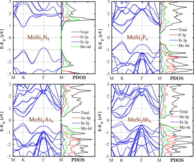

The electrical and spin properties of four materials are summarized in Table 2. First, the band gaps with and without spin-orbit coupling consideration are compared. In the case of MoSi2N4, the band gaps without and with SOC are approximately the same. These values which are in good agreement with experimental work Hong et al. (2020), are 1.73 and 1.721 eV, respectively. The bandgap of MoSi2P4 without(with) SOC is 0.772(0.648) eV that is near to 0.61 eV reported for with SOCAi et al. (2021). The bandgap of MoSi2As4 decreases from 0.664 to 0.525eV with applying spin-orbit coupling, while the values of 0.6eV and 0.41-0.5 eV are reported for without and with spin-orbit coupling consideration, respectivelyHong et al. (2020); Guo et al. (2020); Ai et al. (2021); Li et al. (2020). The SOC has more significant effects on the heavier compounds so that the bandgap reduces by 0.172 eV for MoSi2Sb4 with applying SOC. In addition, the conduction and valence band maximum is presented in the table. In the end, the spin-splitting at K-point in the valence band, the first and second conduction bands are listed in the table. The value of spin-splitting of MoSi2N4 at K-point () of the valence band is 131 meV which is a little smaller than 140 meV from experimental work. However, 130 meV is reported for in the theoretical papers Li et al. (2020). Furthermore, the calculated value of for MoSi2As4 is 0.179 eV and in good agreement with previous reported valuesGuo et al. (2020); Li et al. (2020). increases with changing X-atom from N to Sb and reaches 220 meV for MoSi2Sb4. The spin-splitting at the first conduction band () is not considerable. On the contrary, the second band demonstrates a significant spin-splitting and for example, is larger than in MoSi2N4, but the energy of the second band is much higher than the first band in this compound. The spin-splitting at K-valley in the second conduction band () decreases from 187 meV in MoSi2N4 to 83 meV in MoSi2P4 and increases by changing X atom from P to Sb. By looking at the conduction band of MoSi2As4 and MoSi2Sb4 at K-point, one can find that the first and third bands do not demonstrate remarkable spin-splitting, while the second and fourth display notable spin-splitting.
| E | E | VBM | CBM | EC-EF | EV-EF | ||||||
| (eV) | (eV) | (eV) | (eV) | () | (GPa) | (eV) | (eV) | (eV) | |||
| MoSi2N4 | 1.73 | 1.721 | K | 0.582 | -1.139 | -22 | 25.3 | 0.131 | 0.003 | 0.187 | |
| MoSi2P4 | 0.772 | 0.648 | K | K | 0.333 | -0.315 | -11 | 9.1 | 0.143 | 0.004 | 0.083 |
| MoSi2As4 | 0.664 | 0.525 | K | K | 0.275 | -0.25 | -11 | 8.9 | 0.179 | 0.014 | 0.113 |
| MoSi2Sb4 | 0.481 | 0.309 | K | K | 0.179 | -0.131 | -10 | 7.3 | 0.22 | 0.018 | 0.151 |
| MoSi2N4 | 0.794 | 0.595 | 1.375 | 1.37 | 0.544 | 0.485 |
| MoSi2P4 | 0.562 | 0.388 | 1.483 | 1.335 | 0.697 | 0.567 |
| MoSi2As4 | 0.701 | 0.438 | 1.586 | 1.407 | 1.206 | 0.625 |
| MoSi2Sb4 | 0.925 | 0.447 | 2.288 | 1.992 | 1.843 | 0.647 |
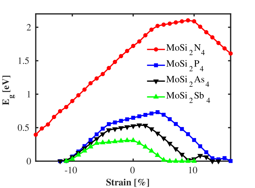
The effective masses of the conduction and valence bands are reported in Table 3. The effective masses of both - and K-points of the valence band are presented in the table. K-point demonstrates a lower effective mass with respect to -one. The anisotropic contour around K-valley leads to two different values at K to M and K to paths. The K to M effective mass () displays a higher value than K to \textGamma effective mass (). On the other hand, \textGamma-point owns isotropic contour, and effective masses at different paths are approximately equal. In Ref. Hong et al., 2020, the effective mass of the electron is reported to be 0.486 m0, which corresponds to our calculated value 0.485 m0 for K to \textGamma path. Furthermore, the reported value of the hole effective mass is 0.683 m0 that is in the middle of our calculated effective masses at K-valley. However, \textGamma-point is the VBM and demonstrates a larger effective masses. Except MoSi2N4, the effective masses for the valence band increase for heavier compounds and MoSi2P4 contains the lowest effective mass. On the other hand, only K-valley contributes to the conduction band. The effective masses at two different paths for this valley are reported in the table. The effective masses in these two paths are in the same range for MoSi2N4 and MoSi2P4, whereas their differences are enhanced for MoSi2As4 and MoSi2Sb4. As mentioned before, the contour around K-valley changes from circular for MoSi2N4 to triangular in MoSi2Sb4. In this regard, MoSi2Sb4 demonstrates high anisotropic effective masses at two different paths. The effective masses of the conduction band increase for the heavier compounds. MoSi2N4 and MoSi2P4 possess the lowest effective mass in the conduction and valence bands, respectively. The vertical strain is known as a powerful tool to modify electrical and spin properties of two-dimensional compounds Ghobadi and Touski (2021); Shamekhi and Ghobadi (2020). This strain can be applied by out-of-plane pressure and 2D materials can be used as a pressure sensor. The vertical strain is applied to the four structures and their electrical and spin properties are studied. First, the variation of the band gaps as a function of vertical strain is depicted in Fig. 5. The band gaps exhibit a maximum value at a specific small tensile strain and then decrease for larger compressive and tensile strains. The band gaps vanish at transition strains (). The value of compressive and its corresponding pressure () are reported in Table 2. The band gaps of MoSi2P4, MoSi2As4 and MoSi2Sb4 vanish around the strain of -10 or -11. On the other hand, MoSi2N4 demonstrates a higher bandgap, and is two times larger at -22 strain. for MoSi2P4, MoSi2As4 and MoSi2Sb4 is in the range of [7.3-9.1] GPa, whereas MoSi2N4 demonstrates much larger of 25.3 GPa. The transition pressures for bilayers are reported from 2.18 GPa in CrSi2N4 to 32.04 GPa in TiSi2N4 Zhong et al. (2021) that are comparable with MoSi2X4 monolayer. This transition pressure range also proves that applying out-of-strain to monolayer MoSi2X4 is feasible. The band gaps also vanish at tensile strain. MoSi2Sb4 demonstrates higher sensitivity to tensile strain and its band gap vanishes at lower strains. The transition strain at tensile regime increases as X atom changes from Sb to N. One can conclude from the figure that tensile transition strain of MoSi2N4 is much larger than 15.
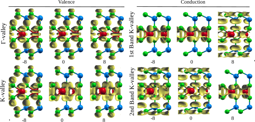
The energies of the K-valleys for the first and second conduction bands, and K- and -points of the valence band versus vertical strain is plotted in Fig. 6. The energies of the up- and down-spins are separately shown in the figure. The strain ranges of the figures are different and the strain ranges are selected in the semiconducting phase. At large compressive strains, the energy of -point of the valence band is higher than K-point and K-valley determines the VBM. By increasing strain from compressive to the tensile regime, the energy of -point decreases, and the energy of K-point increases. One can find the large spin-splitting at K-point, whereas -point does not demonstrate any splitting. On the other hand, two bands contribute to the conduction band. We have called the bands with low and large spin-splitting as -band and -band, respectively. The -band contributes as CBM at compressive and small tensile strains. The larger tensile strains bring down the -band and change the location of these two bands. Therefore, CBM is contributed by -band at a large tensile strain regime. The charge distribution around K- and -points of the valence band and K-valleys of the first and second conduction bands in the case of MoSi2P4 is shown in Fig. 7. A single layer of MoSi2P4 can be divided into three sub-layers. The charge is significantly localized around the Mo atom in the K-point of valence and conduction bands. -point of the valence band has bonding character between P and Si atoms of two sub-layers. In addition, the charge is distributed around the most external P atoms. The out-of-plane strain does not significantly affect charge distribution at this point. In the K-point of the valence band, the charge is highly distributed in the internal MoN2 sub-layer and a small charge is around outer P atoms. At compressive out-of-plane strain, the charge around outer P atoms is expanded. Furthermore, the first and second conduction bands at K-valley are compared in the figure. At equilibrium, the charge is localized in the internal sub-layer for the first band, whereas the charge is distributed in the whole thickness of the compound for the second band. The compressive strain does not affect the charge distribution, whereas tensile strain changes the location and charge density of these two bands.
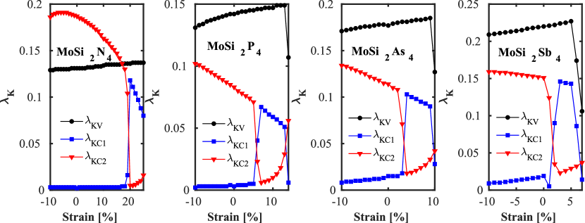
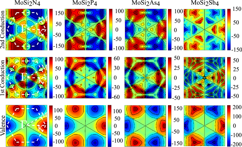
Two-dimensional maps of the spin-splitting in the first Brillouin zone for all compounds have been shown in Fig. 8. Both first and second conduction bands along with the valence band are indicated in the figure. The positive and negative spin-splitting around K and K’-valleys are obvious in the figures, respectively. The first conduction bands of all compounds except MoSi2N4 display a low spin-splitting. In the case of MoSi2N4, a large spin-splitting is around M- and \textGamma-valley, but these two valleys do not contribute to the CBM. One can observe that the spin-splitting of the first conduction band is approximately zero on the boundary of the first Brillouin zone for MoSi2P4 and MoSi2As4. On the contrary, the second conduction band exhibits a high spin-splitting which is located at K- and K’- valleys. MoSi2N4 and MoSi2Sb4 demonstrate a higher spin-splitting compared to the others. ̵ُThe valence band shows a tidy spin-splitting so that the splitting is maximum around K- and K’-valleys and it vanishes elsewhere. The spin-splitting increases for heavier compounds and MoSi2Sb4 show the highest value. We have seen from Table 2 that the valence band of MoSi2Sb4 has the highest spin-splitting as high as 220 meV. The spin-splitting of the valence band is isotropic around the K-valley of MoSi2P4 and other materials specially MoSi2Sb4 demonstrate anisotropic spin-splitting. In this regard, the contour around the K-valley of MoSi2P4 is circular, whereas MoSi2Sb4 has a triangular shape. To clarify the origin of spin-splitting in the valence and conduction bands, the projected band structure of four structures is plotted in Fig. 9. As it is obvious, the first and second conduction bands at K-valley are mainly affected by the d-orbitals of molybdenum atoms. The p-orbitals of X and Si atoms have a low contribution on the first and second bands, respectively. The large spin-splitting of the second band comes from the d-orbitals, whereas the first conduction band with a high d-orbital contribution shows a small splitting. Maybe, this is related to the odd and even bands because the third one also displays a negligible spin-splitting in MoSi2As4 and MoSi2Sb4. In addition, the valence band at K- and \textGamma-points is highly formed by the d-orbitals of Mo atoms. The p-orbitals of X atoms also have a considerable influence at the K-point, whereas p-orbitals of Si atoms contribute to the \textGamma-point. Therefore, the d-orbitals of Mo atoms, the p-orbitals of X and Si atoms have the most impact on the \textGamma-point of the valence band, respectively. The large spin-splitting at valence band is originated from the d-orbitals, whereas the p-orbitals of X atoms enhance the spin-splitting for heavier compounds. The spin-splitting of the K-point of the valence band and the first and second bands of the conduction band versus vertical strain is shown in Fig. 10. increases slightly when strain increases from compressive to tensile regime. The increase of the spin-splitting of the valence band with respect to strain has also observed in the group-III monochalcogenides Ariapour and Touski (2020). One can find from the band structures and Table 2, that the first conduction band has a negligible spin-splitting, while the second band demonstrates a considerable spin-splitting. increases when strain increases from compressive to tensile, whereas decreases. The slope of variation is higher in lighter compounds. As one can observe the curves of and change with each other at the tensile strain. As we have seen in Fig. 6, the -band moves downward and becomes lower than -band for tensile strain. So, in the tensile regime, -band with large spin-splitting is the first conduction band. This band changing is also observed in the figure.
IV conclusion
The electrical and spin properties of monolayer MoSi2X4 (X = N, P, As, and Sb) under vertical strain are investigated. MoSi2N4 demonstrates an indirect bandgap from at valence to K at conduction band, whereas K-valley at valence band is close to -point and contributes to the valence band. On the other hand, three other compounds have direct bandgap at K-point and -point at valence band is also close to K-point. Although the first conduction band demonstrates a small spin-splitting, the second conduction band has a large spin-splitting and its minimum is near to the first band. The PDOS demonstrates that the conduction and valence bands are mostly affected by the d-orbitals of Mo atoms. X atoms have a lower contribution to the valence band. The projected band structure also demonstrates that the conduction and valence bands are mainly constructed from the d-orbitals of Mo atoms. The p-orbitals of X and Si atoms also contribute to the valence and second conduction bands, respectively. The spin-splitting at K-point () of valence band increases with changing X-atom from N to Sb and reaches 220 meV for MoSi2Sb4. The spin-splitting at K-valley in the second conduction band () increases from 83 meV in MoSi2P4 to 151 meV for MoSi2Sb4. In the following, the effect of vertical strain has been investigated. The band gaps exhibit a maximum value at small tensile strains, then they decrease for compressive and larger tensile strains. The band gaps close at compressive transition strains () of around -10 for all compounds except MoSi2N4 that its bandgap vanishes at the larger strain of about -22. Transition pressures are also distributed from 9.1 to 7.3 GPa for MoSi2P4, MoSi2As4 and MoSi2Sb4, whereas MoSi2N4 displays a larger of 25.3 GPa. In addition, the charge is mostly localized around Mo atoms in both valence and conduction bands. The spin-splitting around K-valley at the valence band is isotropic and circular in the case of MoSi2P4, whereas the anisotropy increases for heavier compounds and MoSi2Sb4 exhibits a triangular shape contour. The spin-splitting of K-valley of the valence band increases when strain increases from compressive to tensile regime. increases when strain increases from compressive to tensile, and at the same time, decreases. The slope of variation is higher for the lighter compounds. and change with each other at the tensile strain. In addition to the electrical properties, the vertical strain can also control the spin properties.
References
- Neto et al. (2009) A. C. Neto, F. Guinea, N. M. Peres, K. S. Novoselov, and A. K. Geim, Reviews of modern physics 81, 109 (2009).
- Radisavljevic et al. (2011) B. Radisavljevic, A. Radenovic, J. Brivio, V. Giacometti, and A. Kis, Nature nanotechnology 6, 147 (2011).
- Guan et al. (2014) J. Guan, Z. Zhu, and D. Tománek, Physical review letters 113, 046804 (2014).
- Zhang et al. (2015) S. Zhang, Z. Yan, Y. Li, Z. Chen, and H. Zeng, Angewandte Chemie 127, 3155 (2015).
- Mudd et al. (2013) G. W. Mudd, S. A. Svatek, T. Ren, A. Patanè, O. Makarovsky, L. Eaves, P. H. Beton, Z. D. Kovalyuk, G. V. Lashkarev, Z. R. Kudrynskyi, et al., Advanced Materials 25, 5714 (2013).
- Li et al. (2017) Q. Li, L. He, C. Sun, and X. Zhang, The Journal of Physical Chemistry C 121, 27563 (2017).
- Wang et al. (2016) Y. Wang, S.-S. Wang, Y. Lu, J. Jiang, and S. A. Yang, Nano letters 16, 4576 (2016).
- Ozdemir (2018) B. Ozdemir, Computational Condensed Matter 17, e00335 (2018).
- Hong et al. (2020) Y.-L. Hong, Z. Liu, L. Wang, T. Zhou, W. Ma, C. Xu, S. Feng, L. Chen, M.-L. Chen, D.-M. Sun, et al., Science 369, 670 (2020).
- Wang et al. (2021) L. Wang, Y. Shi, M. Liu, A. Zhang, Y. Hong, R. Li, Q. Gao, M. Chen, W. Ren, H. Cheng, et al., Nature Communications 12 (2021).
- Zhong et al. (2021) H. Zhong, W. Xiong, P. Lv, J. Yu, and S. Yuan, Physical Review B 103, 085124 (2021).
- Li et al. (2021) B. Li, J. Geng, H. Ai, H. Bai, K. H. Lo, K. W. Ng, Y. Kawazoe, H. Pan, et al., Nanoscale (2021).
- Mortazavi et al. (2021) B. Mortazavi, B. Javvaji, F. Shojaei, T. Rabczuk, A. V. Shapeev, and X. Zhuang, Nano Energy 82, 105716 (2021).
- Yu et al. (2021) J. Yu, J. Zhou, X. Wan, and Q. Li, New Journal of Physics 23, 033005 (2021).
- Bafekry et al. (2021a) A. Bafekry, M. Faraji, D. Hoat, M. Shahrokhi, M. Fadlallah, F. Shojaei, S. A. H. Feghhi, M. Ghergherehchi, and D. Gogova, Journal of Physics D: Applied Physics 54, 155303 (2021a).
- Yao et al. (2021) H. Yao, C. Zhang, Q. Wang, J. Li, Y. Yu, F. Xu, B. Wang, and Y. Wei, Nanomaterials 11, 559 (2021).
- Yang et al. (2021) C. Yang, Z. Song, X. Sun, and J. Lu, Physical Review B 103, 035308 (2021).
- Ai et al. (2021) H. Ai, D. Liu, J. Geng, S. Wang, K. H. Lo, and H. Pan, Physical Chemistry Chemical Physics 23, 3144 (2021).
- Nayak et al. (2014) A. P. Nayak, S. Bhattacharyya, J. Zhu, J. Liu, X. Wu, T. Pandey, C. Jin, A. K. Singh, D. Akinwande, and J.-F. Lin, Nature communications 5, 1 (2014).
- Chi et al. (2014) Z.-H. Chi, X.-M. Zhao, H. Zhang, A. F. Goncharov, S. S. Lobanov, T. Kagayama, M. Sakata, and X.-J. Chen, Physical review letters 113, 036802 (2014).
- Ghobadi (2019) N. Ghobadi, Physica E 111, 158 (2019).
- Bafekry et al. (2021b) A. Bafekry, C. Stampfl, M. Naseri, M. M. Fadlallah, M. Faraji, M. Ghergherehchi, D. Gogova, and S. Feghhi, Journal of Applied Physics 129, 155103 (2021b).
- Wu et al. (2021) Q. Wu, L. Cao, Y. S. Ang, and L. K. Ang, Applied Physics Letters 118, 113102 (2021).
- Guo et al. (2020) S.-D. Guo, W.-Q. Mu, Y.-T. Zhu, and X.-Q. Chen, Physical Chemistry Chemical Physics 22, 28359 (2020).
- Soler et al. (2002) J. M. Soler, E. Artacho, J. D. Gale, A. García, J. Junquera, P. Ordejón, and D. Sánchez-Portal, J. Phys.:Condensed Matter 14, 2745 (2002).
- Perdew and Zunger (1981) J. P. Perdew and A. Zunger, Phys. Rev. B 23, 5048 (1981).
- Kokalj (2003) A. Kokalj, 28, 155 (2003).
- Touski and Ghobadi (2020) S. B. Touski and N. Ghobadi, Physica E p. 114407 (2020).
- Ghobadi and Touski (2020) N. Ghobadi and S. B. Touski, Journal of Physics: Condensed Matter 33, 085502 (2020).
- Li et al. (2020) S. Li, W. Wu, X. Feng, S. Guan, W. Feng, Y. Yao, and S. A. Yang, Physical Review B 102, 235435 (2020).
- Ghobadi and Touski (2021) N. Ghobadi and S. B. Touski, Journal of Physics: Condensed Matter (2021).
- Shamekhi and Ghobadi (2020) M. Shamekhi and N. Ghobadi, Physica B 580, 411923 (2020).
- Ariapour and Touski (2020) M. Ariapour and S. B. Touski, Journal of Magnetism and Magnetic Materials 510, 166922 (2020).