Andreev reflection adjusting in the multi-terminal device with the kink states
Abstract
At the domain wall between two regions with the opposite Chern number, there should be the one-dimensional chiral states, which are called as the kink states. The kink states are robust for the lattice deformations. We design a multi-terminal device with the kink states to study the local Andreev reflection and the crossed Andreev reflection. In the three-terminal device the local Andreev reflection can be suppressed completely for either and or and , where is the on-site energy of the graphene terminals and is the stagger energy of the center region. The coefficient of the crossed Andreev reflection can reach in the four-terminal device. Besides adjusting the phase difference between superconductors, the local Andreev reflection and the crossed Andreev reflection can be controlled by changing the on-site energy and the stagger energy in the four-terminal device. Our results give some new ideas to design the quantum device in the future.
I Introduction
Topological insulatorMoore2010 (1) has been one of the noticeable advanced materials due to the novel physical propertiesHasan2010 (2, 3), such as quantum Hall effectLaughlin1981 (4, 5) and quantum spin Hall effectKane2005a (6, 7). It is of great significance to study the properties of topological insulator for developing a new generation of quantum components. Recently, the quantum anomalous Hall effect has been identified in the three-dimensional magnetic topological insulatorYu2010 (8, 9, 10, 11), which opens new possibilities for chiral-edge-state-based devices in zero external magnetic fieldYasuda2017 (12, 13). The chiral states can also appear at the domain walls between two regions with the opposite Chern numberLi2017 (14). For example, the graphene can be gapped by the sublattice symmetry breaking staggered on-site energy, which is showed in Fig. 1. There are one-dimensional statesQiao2011 (15, 16, 17, 18), which are referred to as kink states below, presenting at the boundaries between regions with different quantized Hall conductances in the graphene nanoribbon.
.
A Majorana fermion, which is its own antiparticle, has the potential for quantum computing. Over the last two decades it has been realized that Majorana fermions can emerge at zero-energy modes in topological superconductorsFu2009 (19, 20, 21). After the chiral Majorana edge modes in the quantum anomalous Hall insulator-superconductor structure is realized in the experiment, there are more researches focused on the topological superconductor deviceXie2009 (23, 24, 25, 26, 27, 28, 29).
At the interface between a superconductor and a normal conductor, an incident electron from the normal conductor can be reflected as a hole, which is called Andreev reflection. When the bias voltage is lower than the superconductor gap, the conductance of the superconductor hybrid device is mainly determined by the progress of the Andreev reflection. Keeping to the time-reversal symmetry, the electron and the hole taking part in Andreev reflection come from the different valleys in the graphene-superconductor deviceBeenakker2006 (30, 31, 32).
In this paper, we calculate the transmission coefficients in a two-terminal device, where there are lattice deformations around the domain wall. The transmission coefficients are close to in the two-terminal device, which proves the robustness of the kink statesQiao2011 (15, 16, 17). Then we study the Andreev reflection in the four-terminal device with the topological kink states showed in Fig. 1. Through calculating the coefficients of the Andreev reflection in the four-terminal device, we find that the progress of the crossed Andreev reflection can be controlled by adjusting the on-site energy and the stagger energy.
The rest of this paper is arranged as follows. In Sec.II, the model Hamiltonian for the system is presented and the formulas for calculating the Andreev reflection coefficients are derived. Our main results are shown and discussed in Sec.III. Finally, a brief conclusion is presented in Sec.IV.
II MODEL AND METHOD
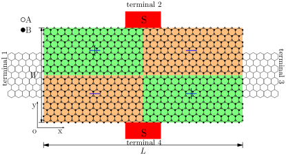
The four-terminal device with the kink states is showed in Fig. 1, where the terminal and are the normal graphene ribbons and the terminal and are superconductors. The center region is the colour region. The kink states are at the interface between the regions with different colour. Along the x direction and the y direction they are zigzag and armchair, respectively. The total Hamiltonian of this junction can be represented as
| (1) |
where, , and are the Hamiltonian of the center region, the graphene nanoribbons, the superconductor terminals and the coupling between the center region and the superconductor terminals, respectively.
In the tight-binding representation, and are given by
| (2) |
where and are the creation operator and annihilation operators of the th point. is the on-site energy in the graphene terminals and the center region. In the center region, for the different partition, where is the stagger energy of A and B sublattice. The second term in Eq. (2) stands for the nearest-neighbor hopping Hamiltonian. Considering that the center region is directly coupled to the superconductor terminals, we use the BCS Hamiltonian for the superconductor terminals described by a continuum model,
| (3) |
where . Here is the superconductor gap and is the superconductor phase. The coupling between superconductor terminals and graphene is described by
| (4) |
Here and represent the positions of the coupling atoms on the interface of superconductor and the center region, and is the annihilation operator in real space. Note that represents the spin index and is the coupling strength between graphene and superconductor terminals.
We now turn to analyze the process that an incident electron from the graphene terminal is reflected into a hole with a Cooper pair emerging in the superconductor terminal. Using nonequilibrium Green’s function method, we can calculate the retarded and advanced Green’s function , where is the Hamiltonian of the center region in the Nambu representation and is the unit matrix with the same dimension as . is the retarded self-energy due to the coupling to the terminal , where is the surface Green’s function of the terminal . We can numerically calculate the surface Green’s function of the graphene terminals. For superconductor terminals, the surface Green’s functionXie2009 (23, 27, 25) in real space is
| (7) |
where and is the density of normal electron states. is the Bessel function of the first kind with the Fermi wavevector . for and for .
The Andreev reflection coefficients for the incident electron coming from the graphene terminal can be obtainedXie2009 (23) by
| (8) |
where the subscripts , , and represent the 11, 22, 12 and 21 matrix elements, respectively, in the Nambu representation. The linewidth function is defined with the aid of self-energy as . and represent the coefficients of the local Andreev reflection and the crossed Andreev reflection, respectively. Because the Andreev reflection from an electron to a hole is equivalent to that from a hole to an electron under particle-hole symmetry, in this work we only consider the Andreev reflection, where an incident electron is reflected as a hole.
III NUMERICAL RESULTS AND ANALYSIS
In numerical calculations, we set the nearest-neighbour hopping energy . The length of the nearest-neighbor C-C bond is set to be as in a real graphene sample. The superconductor gap is set to be and the Fermi wavevector . For the convenience of discussing the influence of the kink states on Andreev reflection, The Fermi energy is set to be zeros in our calculations for the convenient.
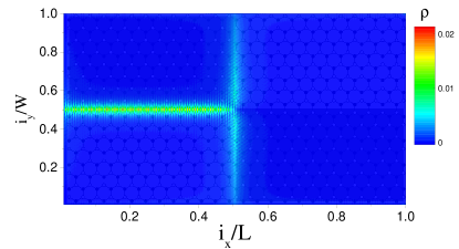
Fig. 2 shows the local density of states contribution of scattering states injected from the terminal when the four terminals connected with the center region are the graphene nanoribbon. From Fig. 2, we can see that in the center region the electrons can only travel along the interface between two regions with the opposite value of stagger energy.It is clear that when the electrons injected from terminal , they can only travel along the kink states into the terminal and the terminal . The propagation to terminal is forbidden. It shows that an electronic beam splitter is created by this design. At the intersection point propagation in the forward direction from the terminal to the terminal is forbidden because of the reversed pseudospin in the direction of propagation along the directionQiao2011 (15), which is explained in the energy band below.
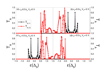
It is certified that how the electrons travel along the kink states in the four-terminal device in Fig. 2. Next we want to know the influences of the kink states on the Andreev reflection. The superconductor gap is set to be , which is more less than the stagger energy , so that only kink states take part in the progress of Andreev reflection. Firstly, we study a three-terminal superconductor device, where only one superconductor terminal or is retained in the four-terminal device, which is showed in Fig. 1. The coefficients of the local Andreev reflection and the crossed Andreev reflection varying with the incident energy in the three-terminal device are presented in Fig. 3.
In Fig. 3 (a), when and , the coefficient of local Andreev reflection is , so the local Andreev reflection is suppressed. The coefficient of the crossed Andreev reflection is zero for . When the incident energy increases to , changes from to quickly, then oscillates with increasing. reaches the peak value about when increases to . With increasing more than , decreases quickly. Fixing the on-site energy and adjusting the stagger energy to in Fig. 3 (b), we can see that there is the local Andreev reflection arising for . is symmetrical about the point and reaches the peak value at the points of . is zero for . When the incident energy decreases from , increases to the peak value quickly and oscillates with decreasing. reaches the second highest peak value about at , then decreases quickly with decreasing less than . When the stagger energy is set to be and the on-site energy is , the curves in Fig. 3 (c) are the same as the mirror image of that in Fig. 3 (b). Setting and , we find that the local Andreev reflection is suppressed again and the curve of in Fig. 3 (d) is the same as the mirror image of that in Fig. 3 (a).
In Fig. 3, are a critical points between and . In Fig. 3 (a) and (d) the local Andreev reflection is suppressed and the crossed Andreev reflection takes place for in Fig. 3 (a) and in Fig. 3 (d). In Fig. 3 (b) and (c), is nonzero for . is zeros for and in Fig. 3 (b) and (c), respectively. When the sign of the on-site energy and the stagger energy are set to be same, the local Andreev reflection is suppressed. To sum up, the progress of Andreev reflection can be controlled by adjusting the on-site energy and the stagger energy in the device with kink states.
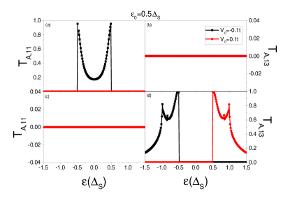
Then when we set the on-site energy , the coefficients of Andreev reflection in the four-terminal device are showed in Fig. 4 for . In the previous works, Andreev reflection can be adjusted by the phase difference of the superconductor terminals in the four-terminal devicecheng2009 (33, 34). The local Andreev reflection is suppressed when , conversely, the crossed Andreev reflection is suppressed when . In Fig. 4 (b) and (c), it is clear that the crossed Andreev reflection is suppressed for and the local Andreev reflection is suppressed for . These results are in accord with the previous workcheng2009 (33, 35). It is important to note that in Fig. 4 (a) for is always zero when , which is different from the results of the previous works. That is to say when the local Andreev reflection can be suppressed by adjusting the stagger energy. In Fig. 4 (d), for , when , keeps zero for ; on the contrary, when , keeps zero for .
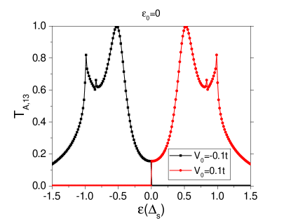
After that, the on-site energy is set to be zero. In Fig. 5, as the incident energy changing the coefficients of the crossed Andreev reflection in the four-terminal device are showed for the on-site energy with . When , the coefficient is zero for the incident energy . Increasing the incident energy, the coefficient changes from to rapidly. When comes up to , the coefficient reaches the peak. Continuing increasing , the coefficient decreases gradually. When , is zero for and reaches the peak at . The peak value of the coefficients can reach at , namely all of the reflected hole can transport into terminal in this device in some conditions. To explain this case we plot the energy band structures of the terminal and the center region in Fig. 6.
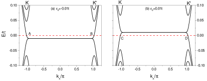
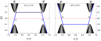
Fig. 6 (a) and (b) are the energy band structures of the terminal and with . Fig. 6 (c) and (d) are the energy bands of the center region with opposite stagger energy, respectively. In Fig. 7 (a), the point A and B are in the conduction band. The point A is in the valley and represents the state of outgoing. The point B is in the valley and represents the state of incoming. In Fig. 6 (b), the point C and D are in valence band. The point C in the valley K represents the state of incoming and the point D in valley represents the state of outgoing. Similarly, in Fig. 6 (c) and (d) the point O and R (P and Q) represent the state of incoming (outgoing), which belong to the valley and , respectively.
When the incident electrons from terminal travel into the center region, which come from the point in the conduction band, they can transport into the point or the point due to the conservation of the momentum. Beside the conservation of the momentum, the travel of the electron must make the pseudospin invariant. So the transport from the point to the point is forbidden and the incident electrons from the point can only travel into the point . In other words, for the low-potential regions, when the incident electrons coming from the valley (the conduction band) or (the valence band) travel into the center region, they should travel into the same valley in the band of center region with the kink states, otherwise, propagation is forbidden. It can explain why the propagation is forbidden in Fig. 2. In Fig. 5, when the incident energy , the electrons come from the point in the conduction band. So the incident electrons can only travel into point R for and the propagation of the electrons is forbidden for in this case.
There is another question to answer. When the local Andreev reflection is suppressed and is zeros for which is beneficial for the crossed Andreev reflection in the four-terminal device. However, we find that for , which is beneficial for the local Andreev reflection, the coefficient is always zeros when . The figure is not showed in the paper.
What is the reason of this case? From Fig. 2, we know that the incident electrons with travel along the kink states to the interfaces between the center region and the superconductors. The reflected holes with must travel along the kink states, too. From our discussions, we know that due to the conservation of the momentum and the pseudospin, propagation of the incident electrons can be forbidden in some conditions. The same reason applies to propagation of the reflected holes. For example, when , the incident electrons from the valley can travel into the center region along the zigzag kink states for and . As the incident electrons flow into the superconductor along the armchair kink states, the reflected holes with travel back to the center region along the armchair kink states. At the intersection, along the zigzag kink states the reflected holes flowing in the direction belongs to the valley and can not flow into the terminal . So the reflected holes flowing in the direction, which belong to the valley , can only travel into the terminal .
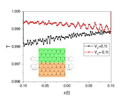
The lattice deformations around the interface are common in the real device. There is a question how the lattice deformations influence the kink states. The two-terminal device with the kink states is showed in the inset of Fig. 7. Considering the deformations of the lattices near the interface, we calculate the transmission coefficients for to answer the question. The transmission coefficient is , where and represents the terminal and in the two-terminal device, respectively. We set the deformation of the lattice to be a random value in the range of . The processes of the calculation are cycled for times and the average values are showed in Fig. 7. Due to the lattice deformation, there should be scattering effect at the interface, the transport coefficients are a little less than for the stagger energy or . From the Fig. 7, we can see that the influence of the lattice deformation on transport is very slight, the minimum value of the transport coefficients is about , which is very close to . The kink states are robust, so it is a good choice for designing quantum devices.
IV CONCLUSIONS
We study the influence of the lattice deformations on the kink states in a two-terminal device. Through our research, we certify that the lattice deformations could weaken the electron transport along the kink states, but the influence is very small. So the kink states are robustness under the lattice deformations.
In the three-terminal device, we find that through adjusting the on-site energy and the stagger energy, for example and , the local Andreev reflection can be completely suppressed. In the four-terminal device, due to the conservation of the momentum and the pseudospin, both the local Andreev reflection and the crossed Andreev reflection can be suppressed when and . This results show us that the progress of Andreev reflection can be controlled by adjusting the on-site energy and the stagger energy in the multi-terminal device with the kink states. It should give us some new ideas on the research and development of the quantum device.
Acknowledgements.
This work was supported by the National Natural Science Foundation of China (Grant Nos. 11874139, 11474085), the Natural Science Foundation of Hebei (Grant Nos. A2017205108, A2019205190), the youth talent support program of Hebei education department (Grant No. BJ2014038), the Outstanding Youth Foundation of HBTU (Grant No. L2016J01), the science program of Shijiazhuang (Grant No. 201790741), the youth talent support program of Hebei Province, and Doctoral Research Foundation of Shijiazhuang College (Grant No. 20BS017).References
-
(1)
Corresponding authors:
1102029@sjzc.edu.cn; yxli@hebtu.edu.cn - (2) J. E. Moore, Nature. 464, 194 (2010).
- (3) M. Z. Hasan and C. L. Kane, Rev. Mod. Phys. 82, 3045 (2010).
- (4) X. L. Qi and S. C. Zhang, Rev. Mod. Phys. 83, 1057 (2010).
- (5) R. B. Laughlin,, Phys. Rev. B. 23, 5632 (1981).
- (6) D. J. Thouless, M. Kohmoto, M. P. Nightingale, and M. den Nijs, Phys. Rev. Lett. 49, 405 (1982).
- (7) C. L. Kane, and E. J. Mele, Phys. Rev. Lett. 95, 226801 (2005).
- (8) C. L. Kane, and E. J. Mele, , Rev. Lett. 95, 146802 (2005).
- (9) R. Yu, W. Zhang, H. J. Zhang, S. C. Zhang, X. Dai, and Z. Fang, Science 329, 61 (2010).
- (10) C. Z. Chang, J. S. Zhang, X. Feng, J. Shen, Z. C. Zhang, M. H. Guo, K. Li, Y. B.o Ou, P. Wei, L. L. Wang, Z. Q. Ji, Y. Feng, S. H. Ji, X. Chen, J. F. Jia, X. Dai, Z. Fang, S. C. Zhang, K. He, Y. Y. Wang, L. Lu, X. C. Ma, and Q. K. Xue, Science 340, 167 (2013).
- (11) J. G. Checkelsky, R. Yoshimi, A. Tsukazaki, K. S. Takahashi, Y. Kozuka, J. Falson, M. Kawasaki, and Y. Tokura, Nature Physics 10, 731 (2014).
- (12) X. F. Kou, S. T. Guo, Y. B. Fan, L. Pan, M. R. Lang, Y. Jiang, Q.M. Shao, T. X. Nie, K. Murata, J. S. Tang, Y. Wang, L. He, T. K. Lee, W. L. Lee, and K. L. Wang, Phys. Rev. Lett. 113, 137201 (2014).
- (13) K. Yasuda, M. Mogi, R. Yoshimi, A. Tsukazaki, K. S. Takahashi, M. Kawasaki, F. Kagawa, and Y. Tokura, Science 358, 1311 (2017).
- (14) M. Mogi, M. Kawamura, R. Yoshimi, A. Tsukazaki, Y. Kozuka, N. Shirakawa, K. S. Takahashi, M. Kawasaki,and Y. Tokura, Nat. Mater. 16, 516 (2017).
- (15) J. Li, R. X. Zhang, Z. X. Yin, J. X. Zhang, K. Watanabe, T. Taniguchi, C. X. Liu, and J. Zhu, Science 362, 1149 (2018).
- (16) Z. H. Qiao, J. Jung, Q. Niu, and A. H. MacDonald, Nano lett. 11, 3453 (2011).
- (17) J. Jung, F. Zhang, Z. H. Qiao, and A. H. MacDonald, Phys. Rev. B 84, 075418 (2011).
- (18) Z. H. Qiao, J. Jung, C. W. Lin, Y. F. Ren, A. H. MacDonald and Q. Niu, Phys. Rev. B 112, 206601 (2014).
- (19) S. G. Cheng, H. W. Liu, H. Jiang, Q. F. Sun, and X. C. Xie, Phys. Rev. Lett. 121, 156801 (2018).
- (20) L. Fu and C. L. Kane, Phys. Rev. Lett. 102, 216403 (2009).
- (21) C. W. J. Beenakker, Rev. Mod. Phys. 87, 1037 (2015).
- (22) S. R. Elliott, and M. Franz, Rev. Mod. Phys. 87, 137 (2015).
- (23) Q. L. He, L. Pan, A. L. Stern, E. C. Burks, X. Y. Che,G. Yin, J. Wang, B. Lian, Q. Zhou, E. S. Choi, K. Murata, X. F. Kou, Z. J. Chen, T. X. Nie,Q. M. Shao, Y. B. Fan, S. C. Zhang, K. Liu, J. Xia,and K. L. Wang, Science. 357, 294 (2017).
- (24) Q. F. Sun and X. C. Xie, J. Phys.: Condens. Matter 21, 344204 (2009).
- (25) Z. Hou, and Q. F. Sun, Phys. Rev. B 96, 155305 (2017).
- (26) J. Liu, H. W. Liu, J. T. Song, Q. F. Sun and X. C. Xie, Phys. Rev. B 96, 045401 (2017).
- (27) M. J. Pacholski, C. W. J. Beenakker, and I. Adagideli, Phys. Rev. Lett 121, 037701 (2018).
- (28) C. Wang, Y. L. Zou, J. T. Song and Y. X. Li, Phys. Rev. B 98, 035403 (2018).
- (29) Hai-Bin Wu, Ying-Tao Zhang and Jian-Jun Liu, Journal of Applied Physics 124, 084301 (2018).
- (30) Hai-Bin Wu and Jian-Jun Liu, Phys. Rev. B 103, 115430 (2021).
- (31) C. W. J. Beenakker, Phys. Rev. Lett. 97, 067007 (2006).
- (32) C. W. J. Beenakker, Rev. Mod. Phys. 80, 1337 (2006).
- (33) C. Wang, L. Zhang, P. P. Zhang, J. T. Song and Y. X. Li, Phys. Rev. B 101, 045407 (2020).
- (34) S. G. Cheng, Y. Xing, J. Wang, and Q. F. Sun, Phys. Rev. B 103, 167003 (2009)
- (35) Y. X. Xing, J. Wang, and Q. F. Sun, Phys. Rev. B 83, 205418 (2011)
- (36) F. Li and S. G. Cheng, J. Phys.: Condens. Matter 27, 125002 (2015).