CODIC: A Low-Cost Substrate for Enabling
Custom In-DRAM Functionalities and Optimizations
Abstract
DRAM is the dominant main memory technology used in modern computing systems. Computing systems implement a memory controller that interfaces with DRAM via DRAM commands. DRAM executes the given commands using internal components (e.g., access transistors, sense amplifiers) that are orchestrated by DRAM internal timings, which are fixed for each DRAM command. Unfortunately, the use of fixed internal timings limits the types of operations that DRAM can perform and hinders the implementation of new functionalities and custom mechanisms that improve DRAM reliability, performance and energy. To overcome these limitations, we propose enabling programmable DRAM internal timings for controlling in-DRAM components.
To this end, we design CODIC, a new low-cost DRAM substrate that enables fine-grained control over four previously fixed internal DRAM timings that are key to many DRAM operations. We implement CODIC with only minimal changes to the DRAM chip and the DDRx interface. To demonstrate the potential of CODIC, we propose two new CODIC-based security mechanisms that outperform state-of-the-art mechanisms in several ways: (1) a new DRAM Physical Unclonable Function (PUF) that is more robust and has significantly higher throughput than state-of-the-art DRAM PUFs, and (2) the first cold boot attack prevention mechanism that does not introduce any performance or energy overheads at runtime.
1 Introduction
DRAM is the ubiquitous technology employed for main memory across computing systems. System components interact with DRAM via DRAM commands. These commands trigger a set of internal DRAM circuit signals that control different DRAM components in a timely manner to achieve a specific functionality (e.g., activate a DRAM row). The timing with which these signals are triggered and the relative order of these signals determine the functionality, energy consumption, and latency of the resulting operation. On modern DRAM devices, the manufacturer fixes these timings at design time for each command. However, having fixed internal circuit timings for each DRAM operation limits the operations that the internal DRAM circuits can perform and hinders their potential for implementing custom optimizations that adapt to the characteristics of the device (e.g., process variation) and environmental conditions (e.g., temperature changes, aging).
The lack of control over internal DRAM circuit timings inhibits at least two research directions. First, prior works that extend the functionalities of DRAM [136, 133, 44, 134, 82, 80, 63, 33, 61, 135] cannot be evaluated or demonstrated reliably on real DRAM chips due to the lack of control over the DRAM internal circuit timing [76]. One example of this limitation is ComputeDRAM [44], which demonstrates computing capabilities in DRAM by triggering a specific sequence of commands from the memory controller with modified timing parameters. Although ComputeDRAM shows the potential for extending functionality by varying standard DRAM operating timings, the results shown in the paper demonstrate that only a small fraction of the cells can reliably perform the intended computations; for a vast majority of cells the intended computation cannot be performed reliably. The reason for this unreliability remains unknown, in part because of the black-box design of DRAM that completely limits the user’s visibility into and control over the DRAM internal timing signals.
Second, several works propose DRAM energy and access latency optimizations by reducing timing parameters of commands issued by the memory controller [88, 61, 29, 172, 89, 162, 81, 87]. However, these works are limited to modifications to memory controller timing parameters, and they do not explore optimizations of internal in-DRAM timing signals. For example, an activate command might have a very conservative time interval between (1) the internal in-DRAM signals that activate the access transistors of DRAM cells, and (2) the internal in-DRAM signals that activate the sense amplifiers (SA) for sensing and amplifying the content of DRAM cells. Reducing this time interval for the DRAM regions that can reliably operate with reduced in-DRAM timings can further improve overall system performance.
In this work, we advocate for a substrate that enables greater control over DRAM internal circuit timings as an efficient and low-cost way to enable new functionalities and optimizations in DRAM. We propose CODIC,111Fine-grained COntrol over DRAM Internal Circuit timings (CODIC). a low-cost DRAM substrate that enables fine-grained control of four key signals that orchestrate DRAM internal circuit timings. The circuits controlled by CODIC perform fundamental operations that (1) connect DRAM cells to bitlines, (2) trigger sense amplifiers, and (3) trigger the logic to prepare DRAM banks for the next access. The memory controller can access the substrate with a new CODIC command, which can be configured with in-DRAM registers to enable new functionalities and optimizations.
By providing fine-granularity control over DRAM internal circuit timings, CODIC enables new DRAM functionalities and optimizations of existing DRAM commands. To demonstrate this point, we implement and evaluate in detail two configurations of the CODIC substrate that expose two new functionalities: (1) in-place generation of digital signatures, which depend on process variation and are unique to each DRAM region and DRAM device (i.e., Physical Unclonable Functions, PUFs [46, 95, 149, 80]); and (2) in-place generation of deterministic values, which are defined at DRAM design-time. These two functionalities are key for implementing several security applications.
Although CODIC can be used for multiple purposes, such as reducing DRAM latency and energy or improving existing DRAM mechanisms (see Section 5), we find that CODIC can be very useful for improving the security of two specific emerging computing platforms. First, low-power systems (e.g., Internet of Things or IoT devices) cannot afford sophisticated security mechanisms adopted by high-end processors (e.g., memory encryption [35]) because such mechanisms can consume significant energy and area [173]. Second, Processing-In-Memory (PIM) systems (e.g., [8, 9, 94, 136, 133, 109, 47, 139, 108, 48, 138, 56, 135, 134, 112, 50, 24, 23, 22, 43, 148, 74, 49]) implement low-cost computing units that typically do not have security features and lack an interface to access the security features of the host processor. For both types of systems, CODIC enables implementing security support within DRAM, thereby enabling suitable applications for improving system security at low-cost.
As a proof of concept, we use CODIC to develop two new applications for improving system security. First, we propose a new CODIC-based Physical Unclonable Function (PUF) [46, 95, 149, 80] with greater throughput and reliability than state-of-the-art DRAM PUFs [80, 153]. A PUF generates signatures unique to a device due to the unique physical variations of the device (i.e., process variation). PUFs are typically used to authenticate or uniquely identify a device. Our evaluation shows that our CODIC-based PUF provides higher throughput, excellent resilience to temperature changes, and more stable PUF responses (i.e., the same challenge produces the same response) than the state-of-the-art DRAM PUFs [80, 153].
Second, we propose a new CODIC-based mechanism to prevent Cold Boot Attacks [170, 57, 143, 52, 17, 107, 160, 104, 96, 91, 65]. In a Cold Boot Attack, the attacker physically removes the DRAM module from the victim system and places it in a system under their control to extract secret information. Because data in DRAM is stored in capacitors, the data can potentially remain in the cells long enough (during physical extraction) for data to be stolen. The key idea of our CODIC-based mechanism is to automatically overwrite the entire DRAM with values generated by CODIC when the DRAM chip is first powered-on. Our evaluation shows that our CODIC-based mechanism is 2.0 faster than the best prior mechanism.
The potential of CODIC extends beyond the security applications proposed and evaluated in this work. CODIC provides a low-cost substrate for controlling DRAM internal circuit timings that enables the implementation of a wide variety of new functionalities, and custom optimizations that improve reliability, performance, and energy consumption. Section 5.3 discusses several other potential CODIC use cases.
We make the following major contributions:
-
•
We propose CODIC, a new low-cost DRAM substrate for controlling DRAM internal circuit timings. CODIC can be used to implement new functionalities, and custom optimizations that improve reliability, performance, and energy consumption. To demonstrate the potential of CODIC, we propose and evaluate two configurations of the CODIC mechanism that enable new security applications.
-
•
We propose a new CODIC-based DRAM PUF that has 1.8 higher throughput than the best state-of-the-art DRAM PUF, has similar resilience to temperature changes, and provides more repeatable PUF responses than the state-of-the-art DRAM PUF. We evaluate our CODIC-based DRAM PUF using 136 real commodity DRAM chips to validate the functionality of our mechanism.
-
•
We propose a new CODIC-based cold boot attack prevention mechanism that operates only at power-on while ensuring reliable protection. Our mechanism does not incur any latency or power overhead at runtime, and it is 2.0 lower latency and 1.7 lower energy than the best state-of-the-art mechanisms [27, 133] during DRAM power-on.
2 Background
DRAM Organization. A single DRAM chip has limited capacity (e.g., 8Gb) and data width (e.g., 8-bit). DRAM chips are grouped together in a DRAM module to form a rank, providing higher capacity (e.g., 8GB) and larger data width (e.g., 64-bit).
Each DRAM rank consists of multiple logical banks striped across chips. Each bank contains multiple (typically 128 to 512) 2D DRAM cell arrays (i.e., subarrays [86, 28]). Cells are organized in rows, which are connected to a row buffer (RB). The RB consists of a set of sense amplifiers that are used to activate one row at a time in the subarray. Each vertical line of cells is connected to one sense amplifier via a bitline wire. Cells within a row share a wordline. Each cell consists of a capacitor that stores data in form of charge ( or V), and an access transistor controlled by the wordline that connects the cell to the Sense Amplifier through the bitline.
DRAM Sense Amplifier (SA). The Sense Amplifier (SA) is used to sense and amplify the small amount of charge in a DRAM cell capacitor to a CMOS-readable value. A set of SAs connected to a row of cells is called row buffer. A cell is connected to an SA via a bitline. In the idle state, bitlines are driven to /2. When the SA is enabled, it detects any voltage deviation from /2 and amplifies the bitline charge to 0 or .
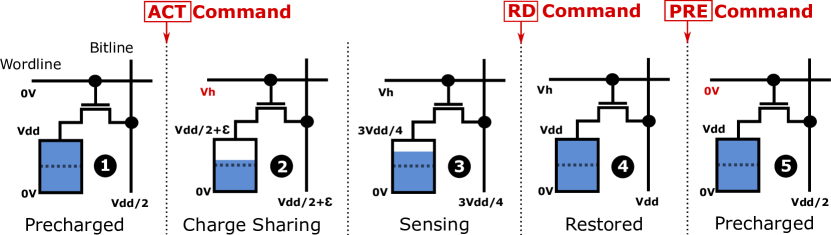
DRAM Operation. The memory controller interacts with DRAM using three basic commands: Activate (ACT), Read/Write (RD/WR), Precharge (PRE). Figure 1 details the steps for reading a DRAM cell using these commands. Initially, the bitline is held at /2 with the wordline at 0V. To access data, the memory controller issues an ACT command, which applies high voltage to the target wordline, connecting that row’s cells to their respective bitlines. This causes a deviation of the bitline voltage in one direction (i.e., in Figure 1, ). This process is called charge sharing. Shortly after, the sense amplifier is enabled to sense and amplify this deviation (3/4 voltage represents an example of a voltage that is not fully amplified). After sufficient amplification, the memory controller can issue RD or WR commands to the row buffer (i.e., sense amplifiers). The time needed to finish the ACT command is specified by the timing parameter . The sense amplifier continues to amplify the deviation until the voltage of the cell is fully restored (i.e., ). Finally, the memory controller issues a PRE command to lower the wordline voltage back to 0V and drive the sense amplifier and bitline to /2. The time needed to complete a PRE command is specified by the timing parameter . Once precharged, another row in the subarray can be activated.
DRAM Internal Circuit Timings. Figure 2a shows a detailed circuit of a common SA design [76], and the four internal DRAM signals required to perform the activate and precharge commands: (1) wl controls the access transistor that connects the cell capacitor to the bitline, (2) EQ controls the precharge unit that sets the bitline to , (3) sense_p controls the PMOS amplifier in the SA, and (4) sense_n controls the NMOS amplifier in the SA.
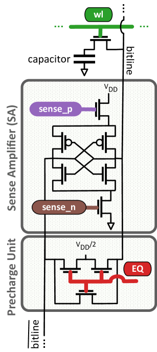
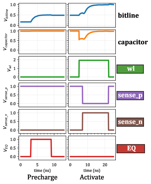
Figure 2b shows the SPICE simulation of the four DRAM internal signals used to implement the precharge and activate commands, and their effect on the voltage of the bitline and the cell capacitor. During a PRE command, we observe that only the EQ signal is triggered for setting the bitline to the precharge voltage level (). During the ACT command, we observe that (1) the wordline (wl) is triggered to share the charge between the cell and the bitline; and (2) after charge sharing, sense_n and sense_p are triggered to sense and amplify the small charge in the cell.
3 Motivation and Goal
Many recent works reveal via DRAM characterization that exploiting the effects of changing timings between DRAM commands can provide substantial benefits to the overall system [88, 61, 29, 172, 89, 162, 81, 87]. However, prior works do not discuss the potential of controlling DRAM internal circuit timings.
Violating Memory Controller DDRx Timing Parameters. We identify and describe three ways in which prior works exploit the ability to violate memory controller DDRx timing parameters [72]. First, prior works [88, 61, 29, 172, 89, 162, 81, 87] identify substantial margins in memory controller DDRx timing parameters (i.e., DRAM latency settings) that can be reduced to improve overall system performance. For example, Chang et al. [29] experimentally demonstrate that they can statically profile DRAM and reduce tRCD while maintaining data correctness. Second, prior works [80, 153, 82, 111] exploit the characteristics of DRAM failures induced by accesses with reduced memory controller DDRx timing parameters, to implement security features such as True Random Number Generators (TRNGs) and Physical Unclonable Functions (PUFs). Third, Chang et al. [30] experimentally demonstrate that they can improve the reliability of DRAM while operating at low voltages by increasing the memory controller DDRx timing parameters.
Limitations of Fixed DRAM Internal Circuit Timings. While characterization of real devices in prior works has lead to important insights, these works are largely limited by the amount of control that the memory controller has over DRAM internal circuit timings. We identify and describe two limitations of current DRAM designs and the DDRx interface.
First, DRAM internal circuit timings (see Section 2) are chosen at design time and cannot be modified. DRAM manufacturers use very conservative internal circuit timings for implementing commands within DRAM (e.g., activate command) with the goal of ensuring reliable operation under worst case conditions. Fixed DRAM internal circuit timings (1) limit the ability to potentially further optimize DRAM commands when accounting for environmental conditions (e.g., temperature) or process variation within a DRAM device to improve DRAM latency (e.g., [88, 61, 29, 172, 89, 162, 81, 87]), and (2) prevent the modification of these internal circuit timings, which can otherwise enable new functionalities [136, 133, 44, 134, 82, 80, 63, 33, 61, 135] and research directions, as we demonstrate in this paper (see Section 5).
Second, memory controller DDRx timing parameters can only control the time between issuing two DRAM commands. Although the memory controller can issue two DRAM commands with accurate timings, it does not have any knowledge or control over the internal implementation of DRAM commands, which limits the control and understanding of the effects of reducing DDRx timing parameters. For example, if an ACT command is issued with reduced DDRx timing parameters after a PRE command, the memory controller does not know the internal DRAM state of the on-going PRE command, which might have not finish its execution in DRAM when the ACT command is issued.
The Potential of Controlling DRAM Internal Circuit Timings. Manufacturers provide a rigid design without any type of control over the DRAM internal circuit timings. We advocate that having more control over the DRAM internal circuit timings has a lot of potential for enabling more aggressive performance, reliability, and energy optimizations, new functionalities, and may open new areas of research.
Goal. Our goal in this paper is two-fold. First, we aim to provide a low-cost substrate in DRAM (called CODIC) that enables fine-grained control over DRAM internal signal timings, for enabling new and enhancing existing DRAM commands and optimizations (Section 4). Second, as a proof of concept, we design two new security mechanisms using CODIC that provide stronger security guarantees and higher performance over state-of-the-art mechanisms (Section 5).
4 CODIC Substrate
We propose Fine-Grained Control Over DRAM Internal Circuit Timings (CODIC), a new DRAM substrate that enables the control of four fundamental DRAM internal signals that control specific circuit timings that are otherwise fixed in DRAM. CODIC allows fine-grained control of these signals, which, in turn, enables the implementation of new DRAM functionalities and performance optimizations.
The applications of CODIC are general and many (see Section 5). As a proof of concept, we demonstrate and evaluate two new variants of CODIC that generate (1) deterministic values that are defined at DRAM design-time, or (2) unique digital signatures that depend on process variation. We use CODIC to build two new security applications that improve the state-of-the-art, as discussed in Sections 5.1 and 5.2.
4.1 Implementing New CODIC Variants
CODIC can control four fundamental signals that control key internal circuit timings (wl, EQ, sense_p, and sense_n), which are described in Section 2. CODIC can trigger and disable these signals within a time window of 25ns, at time steps of 1ns (i.e., a signal can be triggered or disabled at [0ns, 1ns, … 24ns] within the time window), which provides flexibility for implementing a wide variety of new commands, features, and optimizations.
Table 1 shows two existing DRAM commands and two new CODIC variants and the timings of the four signals. The third and fourth columns of the table show the signals that are triggered by the command, and the time (in ns) and direction () that each signal is toggled. The two existing commands are the activate and precharge commands [72], and the two new CODIC variants are CODIC-sig, for generating digital signatures that depend on process variation, and CODIC-det, for generating deterministic values in-memory.
| Command | Description | Signal [init, end] | |
| Activation | See Section 2 | wl [5,22] | sense_p [7,22] sense_n [7,22] |
| Precharge | See Section 2 | EQ [5,11] | |
| CODIC-sig | Generates signature values | wl [5,22] | EQ [7,22] |
| CODIC-det | Generates deterministic values | wl [5,22] | sense_p [14,22] sense_n [7,22] |
4.1.1 CODIC-sig
CODIC-sig generates signature values that depend on process variation by sensing and amplifying a DRAM cell that we set to the precharge voltage (). Sense amplifiers detect minor voltage differences above or below . For a cell precharged to , the bit value that the sense amplifier converges to during activation is dependent on uncontrollable, truly-random manufacturing process variation that perturbs the sensed voltage on the bitline. We verify this randomness in Section 6.1.3, by showing that CODIC-sig values generated from 136 real DRAM chips fully pass the NIST randomness tests [123].
Figure 3a shows the SPICE simulation of CODIC-sig. CODIC-sig raises the wl signal (at 5 ns) before it raises the EQ signal (at 7 ns), which drives the cell capacitor towards /2. Because the bitline is initially precharged to /2, it remains at /2 during the operation (i.e., the bitline is in precharged state). Only after the next activation command (not shown in Figure 3a) the DRAM cell will be amplified to zero or one depending on process variation. We also propose CODIC-sig-opt, a CODIC-sig optimization that is based on the key observation that CODIC-sig can set the voltage of the DRAM capacitor to very quickly. Figure 3a shows that the voltage of the capacitor is set to /2 almost immediately after CODIC-sig triggers the EQ signal. Based on this observation, we can terminate the wl and EQ signals much earlier to reduce the latency of the command, without sacrificing reliability. To take advantage of this optimization, the memory controller requires the ability to change the CODIC timing parameters at runtime (Section 4.2).
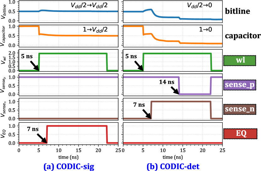
We choose some specific timing values at which the relevant signals are raised such that the operation performs reliably in our simulations. However, other timing values can also perform the same function, e.g., CODIC-sig performs the same function by raising the wl signal at 4 ns, and the EQ signal at 8 ns.
Our SPICE simulations show that CODIC-sig consumes the same power independently of the initial value of the cell (as the final value is always /2). Section 6.1 evaluates the quality of CODIC-sig values (i.e., the quality of CODIC-sig PUF) in real off-the-shelf DRAM chips.
4.1.2 CODIC-det
CODIC-det generates deterministic values. The key idea is to drive the cell to a deterministic value by activating the two signals that drive the SA (sense_n and sense_p) with a delay between them. Depending on which of the two signals triggers first, the generated value is 0 or 1.
Figure 3b shows the SPICE simulation of CODIC-det generating a zero value. CODIC-det triggers the sense_n signal (7 ns), deviating the bitline voltage towards zero. After some delay, CODIC-det triggers the sense_p signal (14 ns). When both signals triggered at the same time, the SA behaves as a regular activation (see Section 2), sensing and amplifying the bitline voltage deviation introduced previously. The value generated with this sequence of signals is deterministic, and always zero. Similarly, for generating a one value, CODIC-det triggers the sense_p (7 ns) signal first, and the sense_n later (14 ns) (not shown in Figure 3b).
4.1.3 Other CODIC Variants
The combination of different timings for triggering/disabling the four control signals enables the implementation of different variants of the CODIC command. For each signal, there is a total of valid combinations of timings.222To calculate the number of variants , we consider that the time step is , and the time window of CODIC is . We sum the number of variants for all signals that start at different timings, i.e., there are 24 variants that trigger at 0ns (the end time can be at 1ns, 2ns… 24ns), 23 variants that trigger at 1ns (the end time can be at 2ns, 3ns… 24ns), etc. Therefore, the total number of different variants is , which is 300 when . For a total of signals, there are valid CODIC variants. The large number of possible combinations provides an enormous design space for optimizing existing DRAM commands and proposing new research ideas. For example, we can use the results of error-characterization studies to optimize a particular DRAM command. To do so, we can re-implement the command using a CODIC variant with timing signals optimized for reliability, performance or energy for a particular DRAM chip.
The number of CODIC variants that result in fundamentally different functionalities is more limited, as the functionality of a particular CODIC command is determined by the relative order in which the internal circuits are triggered and deactivated. During our exploration of the substrate, we have identified other CODIC variants with different properties. For example, by triggering the sense_p and sense_n signals while the bitline is precharged (i.e., without triggering the wl signal), we can create signatures that depend on process variation without destroying the content of the memory cells, unlike CODIC-sig. We do not include the evaluation of this variant because it requires changes to commodity DRAM chips, which makes it very challenging to evaluate in real DRAM chips.
4.2 Implementation Details
Implementing the CODIC substrate in commodity DRAM chips requires minimal changes to (1) the circuit that generates internal timing signals to control internal components in DRAM, and (2) the DRAM interface.
4.2.1 CODIC Circuit Design
To implement the fine-grained configurable control of the timing interval between DRAM internal circuit control signals, we design a configurable delay element using a chain of buffers and a multiplexer, as Figure 4 shows.
We model the delay element using the 22nm PTM transistor model [11] in SPICE. Each buffer stage has a propagation delay of approximately 1ns at the output of the 25-to-1 multiplexer. We estimate the area cost of the circuit by summing up the area of the transistors used for all the buffers and the multiplexer. Assuming a DRAM cell size [120, 129], the area overhead of a configurable delay circuit of CODIC is about 0.28% per mat (a typical mat is 512 rows by 512 columns). The total hardware area overhead for controlling all four DRAM internal control signals (i.e., wl, EQ, sense_n, and sense_p) is per mat.333If needed, we can reduce the area overhead by coarsening the granularity of time control in a CODIC command. The energy overhead of the CODIC circuit design is less than 500fJ, which is negligible compared to the energy consumption of an activation command ( 17nJ). The 2-to-1 multiplexer introduces a negligible delay (0.028ns) to the DDRx activate command, but we compensate for this by sizing the buffers such that the total delay of an activate command is still the same as in the conventional DDRx interface.
The additional logic required to implement CODIC does not affect the operation of common DRAM commands for two reasons: (1) CODIC does not require any changes to the DRAM array, and (2) DRAM commands still use the same logic to generate the internal circuit timings as they do in commodity DRAM chips. For example, as Figure 4 shows, the IS_DDRx signal selects between the fixed delay element for an activation command and the CODIC configurable delay element. A DDRx activate command still uses the conventional fixed delay element to generate a sense_n signal with proper delay after the wl signal.
4.2.2 CODIC Interface
We propose adding a new DRAM command to the DDRx interface to leverage the CODIC substrate using a similar approach to prior academic work [136, 133, 27, 161, 63, 90, 20, 86, 61, 162] and patents [51, 16]. The new CODIC command has the same format as a regular activation. We can integrate the new command in the JEDEC standard specification [72] without extra cost, as there is reserved space for including new commands. By adding a single CODIC command to the DDRx interface, we can implement many different variants of the CODIC command by programming 4 dedicated 10-bit mode registers (MRs) in DRAM, which are used to store the timings of the 4 internal timing signals that CODIC can modify. CODIC uses the existing mode register set (MRS) command defined in the DDRx specification to change the contents of its MR.444JEDEC standard uses mode registers to dynamically change certain DRAM parameters such as burst length, burst type, CAS latency, or DLL reset [72]. To support more than one CODIC variant at the same time, or to allow independent DRAM internal circuit timing configurations for different regions of DRAM, the manufacturer can incorporate more MR registers dedicated to CODIC.
4.3 CODIC Latency and Energy Evaluation
In this section, we study the latency and energy of different variants of the CODIC command.
Methodology. We calculate energy consumption by using the activate and precharge energy consumption described in the power model of the DRAMPower simulator [26].
Latency and Energy Results. Table 2 shows the latency and energy of five CODIC variants that can be implemented with CODIC. We show two CODIC variants that mimic the behavior of regular activation (CODIC-activate) and precharge (CODIC-precharge) commands, our proposed CODIC variants (CODIC-sig, and CODIC-det), and the optimized CODIC-sig variant (CODIC-sig-opt) explained in Section 4.1.1.
| Primitive | Latency (ns) | Energy (nJ) |
| CODIC-activate | 35 | 17.3 |
| CODIC-precharge | 13 | 17.2 |
| CODIC-sig | 35 | 17.2 |
| CODIC-sig-opt | 13 | 17.2 |
| CODIC-det | 35 | 17.2 |
We make two major observations about the latency results. First, CODIC-sig-opt is significantly faster than CODIC-sig, and CODIC-det. However, the CODIC-sig-opt and CODIC-sig latency does not include the additional activation command needed to amplify the DRAM cells to zero or one depending on process variation (see Section 4.1.1). Second, the latency of CODIC-sig and CODIC-det is similar to a standard DDRx ACT command.
Our main observation about the energy results is that they are very similar across all CODIC variants we evaluate for two main reasons. First, all the evaluated variants of CODIC need to route the address within DRAM, which is one of the main sources of energy consumption of all commands (around 40% [26]). Second, the energy consumption of the sense amplifier (used in CODIC-sig) and the precharge logic (used in CODIC-sig) are similar across all commands (around 40% [26]).
4.4 Limitations and Challenges
CODIC is a substrate that can potentially enable many applications, which might introduce application-specific implementation challenges. For example, one of the main challenges to consider when using CODIC PUFs (Section 5.1) is that CODIC works at the granularity of a DRAM row, which could contain data from multiple virtual memory pages (e.g., critical data or data from another process that should not be destroyed). Previous works [136, 133, 137, 27, 56] propose ideas that have similar challenges, and they propose solutions that also could be used with CODIC.
One general concern is that exposing internal signals to users may pose potential security concerns. To preserve CODIC functionality without exposing the internal signals, we can instead provide a more controlled and isolated interface. This interface would provide users with commands to directly invoke the new CODIC applications, instead of allowing the user to access the internals of DRAM directly. For example, the memory controller could provide a direct command for CODIC PUF (Section 5.1) to the user (as either a software API call or as a new assembly instruction). Internally, the controller would keep track of a system-defined memory address range that is safe to use to generate a PUF response, and the controller would internally use CODIC to control the DRAM timings and generate the PUF response. While such an approach prevents user-generated CODIC applications, we can still benefit from new CODIC-based applications that are implemented and exposed by memory controller and CPU manufacturers.
5 Applications Enabled by CODIC
CODIC can be used in many applications. As a proof-of-concept, we design two new applications in the security domain that outperform the best state-of-the-art mechanisms (Section 5.1 and Section 5.2). We also discuss other possible applications that can be implemented with CODIC (Section 5.3).
5.1 Physical Unclonable Functions (PUFs)
A PUF [46, 95, 149, 80] is a hardware primitive that maps a unique input (i.e., challenge) to a unique response. A response is typically derived from the unique physical characteristics (resulting from process variation) of an integrated circuit, such that no two circuits can provide the same response to the same challenge. A PUF can be used as a building block for implementing low-cost authentication protocols [102, 58, 122, 32], key generation applications [101, 171, 114], intellectual property protection [54, 174, 53], hardware obfuscation [165, 78], prevention of reverse engineering [163, 122], intellectual property watermarking [21], software metering [37], or prevention of hardware Trojan embedding [164].
In the specific case of DRAM-based PUFs, one or more parameters (e.g., address and size of a memory segment) define a challenge, and the data read from DRAM is the response to that challenge. Together, they define a Challenge-Response pair (CR pair). In this work, we use the address and size of a memory segment as the only parameters that define a challenge.
Limitations of State-of-the-Art DRAM-based PUFs. Prior DRAM-based PUF proposals exploit variations in DRAM start-up values [155], DRAM write access latencies [60], DRAM cell retention failures [151, 167, 77] and reduced DDRx timing parameters [80, 153]. There are at least four main limitations with most of these approaches. First, most DRAM PUFs [155, 60, 151, 167, 77] have long evaluation times, which may incur significant system interference when the PUF is evaluated at runtime. Second, most DRAM PUFs [155, 60, 151, 167, 77, 80] require heavy filtering mechanisms to deal with the inherently noisy nature of the DRAM responses. Filtering mechanisms increase the reliability of PUF responses at the cost of increasing evaluation latency. Third, the responses to the same challenge in most DRAM PUFs [155, 60, 151, 167, 77, 80] exhibit high variation with temperature changes, which is an important issue in systems with a non-controlled environment (e.g., IoT devices in the wild). Fourth, some DRAM PUFs are data dependent, which may cause the same challenge to have different responses depending on the content of the memory [151, 167, 77, 80, 155, 60].
CODIC-based PUFs. CODIC-sig can generate signature values that depend on process variation and thus can be used as PUF responses (Section 4). CODIC-sig PUF provides four main advantages compared to the state-of-the-art DRAM PUFs. First, CODIC-sig has a fast evaluation time due to its ability to control internal DRAM timing signals. The absence of a filtering mechanism combined with the short latency of CODIC-sig, enables the CODIC-sig PUF to have a shorter evaluation time than the best state-of-the-art DRAM PUF [153]. Second, in contrast to other DRAM PUFs, CODIC-sig does not require any filtering mechanisms because it provides highly stable output values. This stable output allows computing a valid PUF response with a simple low-overhead filter, or without any filter at all (see Section 6.1), depending on the requirements of the application. Third, CODIC-sig has state-of-the-art resilience to temperature changes, i.e., changing the temperature does not influence much the repeatability of the PUF responses. Fourth, CODIC-sig responses do not depend on the content of DRAM, as all DRAM cells are always precharged to for generating a PUF response, independently of their original value.
5.2 Preventing Cold Boot Attacks
A cold boot attack is a physical attack on DRAM that involves hot-swapping a DRAM chip and reading out the contents of the DRAM chip on another system [170, 57, 143, 52, 17, 107, 160, 104, 96, 91, 65]. The attacker first disables power to the computer containing the victim DRAM and then transfers the DRAM to another system that can read its content. Alternatively, the attacker can also recover the memory contents by booting a small special purpose program from a cold reset (i.e., reset after power cycling) [57]. Cold boot attacks are possible because the data stored in DRAM is not immediately lost when the chip is powered-off. This is due to the capacitive nature of DRAM cells that can hold their data up to several seconds [17, 115, 98, 97, 79] or minutes [57]. This data retention effect can be even more significant if the DRAM module is swapped at low temperatures. For this reason, protection mechanisms such as disabling refresh on DRAM for a certain amount of time are not effective at protecting against cold boot attacks.
There are three classes of mechanisms for preventing cold boot attacks. First, mechanisms that rely on encrypting memory either explicitly [150, 12, 168, 41, 121, 64, 75, 170], or implicitly through some CPU extensions (e.g. Intel SGX [35], AMD SEV [6]). These mechanisms are effective and secure, but are complex and expensive (in terms of energy and performance overhead) to be implemented in many low-cost devices. Second, modern systems scramble the data in the memory controller, which helps to obscure the DRAM contents. This mechanism is simple and is also useful for other purposes (e.g., improving signal integrity on the DRAM bus), but it has been shown to be insecure against cold boot attacks [170]. Third, the mechanism proposed by the Trusted Computing Group (TCG) [157] resets the DRAM content upon power-off. This mechanism is implemented on the host platform firmware and depends on the OS, which makes it vulnerable to attacks [116].
We identify at least two scenarios where a fast and secure boot is critically important. First, devices that run intermittently (intermittent computing) [99] extract energy from their environment (e.g., solar energy), and they power-on and execute a burst of operations only once they have enough energy. These devices usually rely on volatile memories such as DRAM [99]. Such devices have very limited energy available to them, and stalling for even a few seconds can reduce the amount of compute possible (and can potentially trigger a greater number of rollbacks). Security is also critically important, because these devices are usually in the wild, and are vulnerable to physical attacks such as cold boot attacks. Second, devices that require instant-on capabilities [31, 92, 147], such as unattended in-the-wild digital cameras that need to power-on instantly when detecting a signal for automatically taking a picture [147].
5.2.1 Threat Model
We assume a threat model in which the attacker has physical access to a live uncompromised machine/device for an unlimited amount of time to steal information stored in the device’s DRAM. In order to successfully read data from DRAM, the attacker cannot keep the DRAM powered-off for long, as this would lead to data loss. We therefore assume that, as part of the attack, the DRAM chip is powered-off for an arbitrarily short amount of time. This power loss occurs either (1) when transplanting the DRAM module to an attacker-controlled machine, or (2) during attacks that reboot the victim machine to load a malicious OS. Note that our threat model does not account for: (1) systems with a warm reboot that never cuts power to DRAM, or (2) hypothetical attacks using a scanning electron microscope (SEM) to read DRAM content.00footnotemark: 055footnotetext: Note that to our knowledge, this attack has not been demonstrated to date on commodity DRAM chips, but only under a controlled environment using custom DRAM samples [145].
5.2.2 Self-Destruction
We make the observation that it is possible to protect from cold boot attacks by deleting all memory contents during the DRAM power-on. Based on this observation, we propose self-destruction, a low-cost in-DRAM mechanism based on CODIC that destroys all DRAM contents without the intervention of the memory controller during DRAM power-on.
The key idea of self-destruction is to destroy the entire DRAM memory using CODIC-sig or CODIC-det. Self-destruction is performed autonomously without the intervention of the memory controller, which could be controlled by the attacker. During self-destruction, the DRAM chip does not accept any memory commands to ensure the atomicity of the process. On a cold boot reset, our mechanism steps through a sequence of CODIC commands in order to destroy the contents of the entire chip sequentially (i.e., row-by-row).
Hardware Implementation. We propose two ways to implement self-destruction within DRAM. First, we propose to add a dedicated circuit that (1) issues CODIC commands back-to-back to all DRAM rows, (2) parallelizes commands across banks, and (3) enforces JEDEC timing constraints (e.g., t_FAW [72]). We evaluate this implementation in Section 6.2. Second, we propose to reuse the existing circuits for self-refresh [71] to issue CODIC commands in our self-destruction mechanism. This implementation is an optimization for reducing the hardware cost, but the destruction time is the same as the time that the self-refresh mechanism takes to refresh the entire memory.
Implementing self-destruction by reusing self-refresh circuits requires two small modifications to the self-refresh circuitry that enhance its default functionality (i.e., self-refresh) to additionally enable it to destroy the contents of DRAM at power-on. First, we add configurable delay circuits (see Figure 4) that generate internal DRAM signals (i.e., wl, sense_p, sense_n, and EQ in Figures 2 and 3) with configurable timings. These newly-generated signals are used to implement the CODIC operations within the self-refresh circuitry. Second, for each connection between an internal DRAM signal (i.e., wl, sense_p, sense_n, EQ) and the DRAM array, we add a MUX that selects whether to use (a) the unmodified signals generated by the self-refresh circuitry for the baseline refresh operation, and (b) our newly-generated signals for enabling data destruction using CODIC. The select line of each MUX is set at power-on (e.g., to 1) to choose the CODIC signals and destroy the DRAM contents, and the select line’s value changes (e.g., to 0) immediately after the entire contents of DRAM are destroyed to enable self-refresh to be used for the rest of the time.
Any implementation of self-destruction also needs logic to trigger the self-destruction mechanism at DRAM power-on.
Security Analysis. Our mechanism is automatically triggered in DRAM when power is detected, without requiring external action. Therefore, the security of self-destruction depends on the reliability of the DRAM module’s power-on detection circuit. There are two ways for an attacker to potentially bypass this circuit. We describe both and explain why, in practice, they do not pose a security threat.
First, an attacker could operate DRAM at low voltage on the compromised system using, for instance, Dynamic Voltage and Frequency Scaling (DVFS)[40, 30, 39, 55], with the goal of not triggering the power-on detection circuit. The power-on circuit triggers when it detects a voltage ramp up from , but the voltage does not need to reach (the power-on circuit triggers as long as a voltage ramp up starting from is detected). Therefore, operating the DRAM at very low voltage would not help the attacker.666The attacker might try to operate the device at a voltage close to such that the power-on circuit cannot detect the ramp up, however, at such low voltage the DRAM chip would not be operational.
Second, an attacker could overheat the DRAM power-on detection mechanism until it stops functioning. In practice, however, the FSM that initializes the chip is in the same internal controller that regulates other functions (i.e., timing signals for activate, precharge, and other commands). Consequently, overheating that component would most likely make the whole DRAM unusable.
5.3 Other Applications
The CODIC substrate enables the implementation of a wide variety of applications. We identify and classify several potential applications into three broad categories, though we note that there may be other applications or categories that can also make use of CODIC.
5.3.1 Security Applications
In Sections 5.1 and 5.2, we propose and evaluate in detail new mitigations mechanisms for two security applications that improve over state-of-the-art. First, CODIC can implement two new Physical Unclonable Functions (PUFs) that improve upon state-of-the-art DRAM PUFs (Section 5.1). Second, CODIC enables the implementation of a new mechanism called self-destruction to protect against cold boot attacks (Section 5.2).
CODIC can also be used to accelerate secure deallocation mechanisms [34, 10, 140, 59, 45]. Secure deallocation is a technique that sets the data to zero at the moment of deallocation, or as soon as the data is not needed anymore, which reduces the time that critical data is exposed to attacks. We evaluate our mechanism and demonstrate that it performs up to 21% better and consumes 34% less energy than secure deallocation techniques implemented in software.
CODIC also enables accurate control of the failure mechanisms used in existing DRAM-based True Random Number Generators (TRNGs) [82, 111, 152] and DRAM PUFs [80, 153]. These mechanisms are triggered by violating the DRAM standards, but the exact internal failure mechanism is not perfectly known (e.g., it might vary depending on the DRAM architecture, timings, manufacturer). A substrate such as CODIC would help to understand and improve the quality and performance of these existing mechanisms, and enable new TRNGs that exploit new failure mechanisms for generating random numbers.
CODIC could also potentially be used to reduce the effectiveness of RowHammer attacks [85, 83, 110, 42, 130]. Because CODIC allows finer-granularity control over DRAM timings, a system designer can potentially adjust the timings of key internal DRAM signals that govern important parameters that affect the susceptibility of a chip to RowHammer, e.g., wordline active time [73].
5.3.2 Custom DRAM Latency/Energy Optimizations
Existing DRAM chips are shipped with fixed and conservative internal circuit timings that guarantee reliable behavior for a wide range of environmental conditions and process variation. Using CODIC, the internal circuit timings can be optimized for a particular DRAM device, based on the device’s current environmental conditions.
Adapting to Environmental Conditions. CODIC enables dynamic and practical adaptation of DRAM internal circuit timings to different environmental conditions (e.g., temperature, voltage, aging), with the goal of optimizing DRAM performance and energy consumption.
Mitigating Process Variation Effects. CODIC enables practical adaptation of DRAM internal circuit timings to process variation of a particular DRAM chip. For example, the retention time of DRAM cells depends on process variation [97, 17, 115, 98, 79, 57]. CODIC can easily provide an alternative activate command for rows with high retention times, which reduces the time between triggering the wordline and triggering the sense amplifier. Using this technique, we enable rows with high retention times to be activated faster during refresh.
Accurate DRAM Characterization. CODIC enables increased precision and opportunities in DRAM characterization. For example, by modifying the time interval between triggering the wl and the sense_p and sense_n signals in an activation command, we can test how fast the cell capacitor shares its charge with the bitline, and infer the relative capacitance of each cell. Such observations would enable us to build more features with a deeper and more accurate understanding of their underlying mechanisms. They can also enable us to build more accurate models of DRAM behavior.
Memory Controller Timing Parameters. CODIC can be used to reliably enforce the usage of reduced memory controller timing parameters (e.g., tRCD), as it enables us to know and control the precise state of one command when the next command is issued with reduced timing parameters. This can better enable prior works [88, 61, 29, 172, 89, 162, 81, 87] to optimize DDRx timing parameters while ensuring robust operation, as the memory controller can make informed decisions about reducing DDRx timing parameters taking into account the DRAM internal state, which is known and can be controlled with CODIC.
5.3.3 Processing-in-Memory (PIM)
PIM proposals such as RowClone [133] and Ambit (bitwise AND, OR) [136, 135, 139] have been demonstrated in real off-the-shelf DRAM chips via manipulating DDRx timing parameters [44]. However, the results shown in [44] demonstrate that many intended computations cannot be performed reliably in a vast majority of chips and cells because it is not possible to control how DRAM commands are executed internally within DRAM chips. An interface like CODIC can more robustly enable RowClone, Ambit, and other PIM mechanisms [56] on real DRAM chips.
6 Evaluation
We evaluate the quality, latency, and randomness of the CODIC PUF (Section 6.1), and the latency and energy of our cold boot attack prevention mechanism (Section 6.2).
6.1 CODIC PUF
We evaluate the quality of the CODIC PUF (i.e., CODIC-sig PUF) responses with a new methodology that allows us to recreate the PUF responses of the CODIC-sig PUF in real off-the-shelf DRAM chips. We perform an exhaustive evaluation using 136 real DDR3 DRAM chips from 15 modules.
Methodology. A CODIC-sig primitive (1) sets a cell to with the precharge logic, and (2) activates the SA to generate a signature value from that cell (as explained in Section 4.1.1). We emulate this behavior in real DRAM chips in two steps. First, based on the observation that a DRAM cell leaks towards , we disable DRAM refresh for 48 hours with the goal of setting the cell to . Second, we activate this cell to obtain the PUF response. This methodology allows us to reproduce the responses that would produce a real CODIC-sig PUF implementation. Recall that discharging the cells with CODIC-sig PUF would take a few nanoseconds (not 48h) in a real implementation (Section 4.3). We perform our experiments with a customized memory controller built with SoftMC [62] and a Xilinx ML605 FPGA on 136 different DDR3 DRAM chips from three major vendors. Table 3 shows the main characteristics of the 136 DRAM chips that we evaluate. Appendix D has more details.
| Vendor | Chips | Capacity/chip | Freq. (MT/s) | Voltage |
| A | 32 | 4Gb | 1600 | 1.35V (DDR3L) |
| A | 32 | 4Gb | 1600 | 1.50V (DDR3) |
| B | 32 | 2Gb | 1333 | 1.50V (DDR3) |
| B | 8 | 4Gb | 1600 | 1.35V (DDR3L) |
| C | 32 | 4Gb | 1600 | 1.35V (DDR3L) |
Evaluating the CODIC-sig PUF functional behavior with our methodology is challenging, because DRAM cells can retain their content for a long time [97, 98, 159, 115, 79], i.e., not refreshing the DRAM does not guarantee that a cell will end up with the precharge voltage (), even after a long period.
To deal with this issue, we tailor a custom test to determine if a cell is set to the precharge voltage. As discussed in Section 4.1.1, when a cell is set to the precharge voltage, the value that CODIC-sig generates should always be the same regardless of the initial value of the cell. Based on this observation, our test analyzes the final value of a DRAM cell after 48 hours without refresh, in two different scenarios: (1) all initial values are zero, and (2) all initial values are one. The test has two possible outcomes. First, the test passes if the final value is the same regardless of the initial value. Thus, we can conclude that the cell is set to the precharge voltage. In this case, the final value is the same as the value that a real CODIC-sig implementation would generate. Second, the test fails if the final value is different from the initial value. In that case, we cannot conclude that the cell is set to the precharge voltage (and thus we cannot infer the value generated by applying CODIC-sig to the cell), so we do not consider that cell in our results.
Following this methodology, we obtain CODIC values for 34% to 99% of all cells in the 136 DDR3 DRAM chips we tested. Most of these cells are always amplified to a particular value (e.g., 0), and the remaining cells (between 0.01% and 0.22% of all cells777We observe that these results are in line with the results obtained in our SPICE simulations (see Section 7.2.1 in [113]).), which are randomly spread across DRAM, are amplified to the opposite value (e.g., 1). We use the addresses of the latter type of cells as PUF responses.
6.1.1 Quality Evaluation
This section evaluates the quality of CODIC PUF responses compared to two state-of-the-art DRAM PUFs [80, 153].
Metrics. To measure the uniqueness and similarity of a PUF, we apply Jaccard indices [70] as suggested by prior works [128, 167, 14, 80]. We determine the Jaccard indices by taking two sets of PUF responses from two memory segments (), and calculating the ratio of their shared values over the full set of the two PUF responses . A ratio close to 1 represents high similarity, and a ratio close to 0 represents uniqueness.
We use the term Intra-Jaccard for representing the similarity of two responses from the same memory segment, and Inter-Jaccard for representing the uniqueness of two responses from different memory segments. An ideal PUF should have an Intra-Jaccard index close to 1 (a unique challenge has a unique response), and an Inter-Jaccard index close to 0 (different challenges have different and random responses).
Methodology. We compute the distribution of Intra- and Inter-Jaccard indices obtained by running experiments on 136 different DRAM chips with segments of 8KB (this size is used by prior work [80]). We calculate the Intra-Jaccard indices for 10,000 random pairs of memory segments (each pair composed of two responses from the same memory segment), and the Inter-Jaccard indices for 10,000 random pairs of memory segments (each pair composed of two responses from different memory segments) from all DRAM chips.
We compare CODIC-sig PUF with the DRAM latency PUF [80] and PreLatPUF [153]. The DRAM Latency PUF accesses DRAM with . For improving the repeatability of the responses, the DRAM latency PUF implements a filtering mechanism that removes cells with low failure probability from the PUF response. To this end, the mechanism reads the memory segment 100 times, and it composes a response that contains only the failures that repeat more than 90 times [80]. PreLatPUF generates PUF responses by reducing the precharge latency ( in our evaluation). The authors of PreLatPUF improve their results by selecting the DRAM cells that are more suitable for PUFs via DRAM characterization. In our evaluation, we do not apply this selection mechanism, as our goal is to compare the quality of the failure mechanisms under the same conditions. Note that the selection mechanism used by the authors of PreLatPUF can be also applied to the DRAM Latency PUF and the CODIC PUF.
The PUF responses generated by CODIC-sig/PreLatPUF are less noisy than the values obtained by DRAM Latency PUF (i.e., the Intra-Jaccard indices are close to one, as we will show in Figure 5 soon), so CODIC-sig/PreLatPUF need a much more lightweight filtering mechanism. Although we experimentally observe that one challenge is enough to get a robust CODIC-sig/PreLatPUF response in most cases (99.72%/96.92% of all challenges have the same response for the worst DRAM module we tested), we apply a conservative filter of 5 challenges for generating always the same response, such that CODIC-sig/PreLatPUF are robust even under worst-case conditions. While a DRAM Latency PUF with a lightweight filtering mechanism (e.g., 1-10 reads) could be as fast as the CODIC PUF, the PUF quality would decrease significantly.
Results. Figure 5 shows the Intra- and Inter-Jaccard indices for the DRAM Latency PUF [80], PreLatPUF [153], and CODIC-sig PUF for 64 DDR3 chips operating at 1.5V and 72 DDR3L chips operating at 1.35V.
We make four main observations. First, the CODIC-sig PUF shows excellent Intra-Jaccard indices (the indices in red, which accumulate close to 1 on the x-axis), and very good Inter-Jaccard indices (the indices in blue, which accumulate close to 0 on the x-axis). Second, the DRAM latency PUF has Intra-Jaccard indices distributed towards 1.0, but the distribution is still very dispersed. The Inter-Jaccard indices of the DRAM Latency PUF are very good; all values are highly concentrated around the zero value (the blue bars). Third, PreLaTPUF shows very good Intra-Jaccard indices (the red bars near 1 on the x-axis), but Inter-Jaccard indices are very dispersed and far from the zero value. Fourth, the results from DDR3L chips are generally better than those from DDR3 chips, especially for the CODIC-sig PUF. We conclude that the CODIC-sig PUF is very effective at providing very similar responses to the same challenge, while maintaining uniqueness across responses to different challenges.
Based on our results, a naive challenge-response authentication mechanism implemented with CODIC-sig that correctly authenticates only when the response is exactly as expected (i.e., no filtering mechanism), has an average false rejection rate of 0.64% and false acceptance rate of 0.00%.
Temperature and Aging Effects. To demonstrate how temperature affects the similarity of different responses to the same challenge. We use the experimental setup from the previous experiment in Figure 5, and the same 136 DDR3 DRAM chips. To control the temperature, we use DRAM heaters on both sides of the DDR3 module, and a fine-grained temperature controller that can control the temperature with a precision of 0.1∘C. We evaluate 4 different temperatures from 30∘C to 85∘C. For this experiment, we wait for only 4 hours (instead of 48), since cells discharge faster at high temperatures [97, 98, 159, 115, 79]. Figure 6 shows the Intra-Jaccard indices between the same segments under different temperatures across 136 chips.
We make three observations. First, the CODIC-sig PUF is very robust to temperature changes, as the responses to the same challenge are very similar even for extreme temperature changes (55∘C). Second, PreLatPUF has the best robustness against temperature changes, but this comes with the trade-off of having poor uniqueness properties, as the Inter-Jaccard indices show in Figure 5. Third, the responses of the DRAM latency PUF are much more sensitive to temperature changes, confirming the results of the original paper [80]. We conclude that the CODIC-sig PUF (1) performs much better than the DRAM Latency PUF under changing temperature conditions, and (2) performs very close to PreLatPUF, which is the most robust PUF against temperature changes.
To demonstrate how aging affects the similarity of different responses to the same challenge, we use accelerated aging techniques to artificially age our DRAM chips [125, 154, 118, 127, 144]. We artificially age the DRAM chips by operating them at 125∘C degrees running stress tests for 8 hours. We observe from our experiments that CODIC-sig PUF is very robust to aging, as most of the Intra-Jaccard indices are 1 (not plotted).
6.1.2 PUF Response Time
Table 4 summarizes the total evaluation time of the three DRAM PUFs. We make two observations. First, the CODIC-sig PUF with/without filter has 20x/100x lower evaluation latency than the DRAM Latency PUF. Second, the CODIC-sig PUF with/without filter is 1.8/1.8 faster than the PreLatPUF. In our evaluation setup, although the filtering mechanism increases CODIC-sig PUF and PreLatPUF evaluation latency, it also avoids other issues related to the no-filter mechanism such as initial profiling to select robust DRAM cells, or metadata accesses required for managing the selected DRAM cells [153]. We conclude that the evaluation time of the CODIC-sig PUF is lower than the best state-of-the-art DRAM PUF.
| Latency PUF | PreLatPUF | CODIC-sig PUF |
| w/(w/o) filter | w/(w/o) filter | |
| 88.2 ms | 7.95 (1.59) ms | 4.41 (0.88) ms |
6.1.3 Randomness Analysis
A secure key or seed should have high-entropy. Although we already demonstrated the uniqueness of the responses between different memory segments (Section 6.1), this does not guarantee that they have high-entropy, and hence that they are suitable to be used as cryptographic keys.
Methodology. We analyze the randomness of the values generated by CODIC-sig with real DRAM chips (Table 12), with the experimental setup of Section 6.1. We use the NIST statistical test suite [123] to analyze the numbers generated by CODIC-sig.
Results. We run the NIST test suite with 250KB random streams composed of responses to different challenges from all tested DRAM chips. We use a Von Neumann extractor [142] for whitening the random stream. Our results show that the numbers generated by CODIC-sig pass all 15 NIST tests, which demonstrates that our PUF is able to generate high-quality random numbers. Appendix B has more details.
6.2 Preventing Cold Boot Attacks
We compare our new CODIC-based self-destruction mechanism (introduced in Section 5.2) to (1) a mechanism that resets the DRAM’s contents by issuing write commands from the memory controller to every single row in a DRAM chip, as described in the TCG specification [157]; (2) a self-destruction mechanism that uses RowClone [133] to copy rows initialized to zero into all other rows in a DRAM chip; and (3) a self-destruction mechanism that uses LISA-clone [27] to copy rows initialized to zero into all other rows in a DRAM chip.
Methodology. We customize Ramulator [84, 126] to support our CODIC implementation, RowClone and LISA-clone. Table 5 shows the summary of the CPU, memory controller, and DRAM parameters used in our evaluation.
| CPU | in-order core, 32KB L1 D&I, 512KB L2 |
| Memory Controller | 64/64-entry read/write queue, FR-FCFS [119, 176] |
| DRAM | 1 channel, DDR3-1600 x8 11/11/11 |
Our baseline is the firmware-based TCG cold boot attack prevention mechanism. We evaluate TCG by simulating the firmware that overwrites the memory with zeros by issuing regular write requests. To force writing back the data to memory from cache, we use an instruction that invalidates the data in cache (i.e., the CLFLUSH instruction in x86 [69]). TCG does not require any hardware changes.
We implement three self-destruction mechanisms (using CODIC, RowClone, and LISA-clone) that perform back-to-back CODIC/RowClone/LISA-clone commands to each DRAM row (parallelized across banks) while meeting the JEDEC timing specifications (e.g., tRCD, tFAW). Note that our CODIC self-destruction mechanism could be further (1) highly-optimized for performance by DRAM vendors, as they know the exact internal DRAM internal power restrictions, or (2) highly-optimized for cost, by reusing the self-refresh circuits, as we describe in Section 5.2.2.888We do not evaluate a self-destruction implementation that reuses the self-refresh circuitry because DRAM vendors do not release details about the implementation of self-refresh. We use the energy and latency of CODIC reported in Table 2 (Section 4). We calculate the energy to destroy contents of the entire DRAM using a customized version of DRAMPower [26]. We calculate the latency to destroy the entire content of DRAM using Ramulator.
Latency Results. Figure 7 shows the destruction time of a TCG software implementation, and three self-destruction mechanisms that respectively use LISA-clone, RowClone, and CODIC to destroy all data in a DRAM module.
We test different DRAM module sizes, from 64MB, used in memories specifically designed for low cost devices [36], to a hypothetical single-rank 64GB.999Existing 64GB DRAM modules today have 4 ranks of 16GB each [106] to avoid excessive refresh overheads [97]. Our simulator takes into account all timing parameters defined by the DDRx standard [72]. The timing parameters for each size are taken from public datasheets released by vendors [105]. For the memories that we do not have enough information about timing parameters (e.g., 64MB, 64GB), we extrapolate the parameters from existing memory modules.
We make two major observations. First, self-destruction using CODIC performs 552.7/2.5/2.0 faster than TCG/LISA-clone/RowClone for an 8 GB DRAM module. Second, the TCG provides lower latency for small memory sizes (e.g., 64MB, 256MB), but the latency for 1GB and larger sizes is prohibitively large.
We conclude that self-destruction using CODIC destroys the entire content of DRAM significantly faster than the best state-of-the-art mechanisms.
Energy Results. Our results show that self-destruction using CODIC consumes 41.7/2.5/1.7 less energy than TCG/LISA-clone/RowClone, for an 8 GB DRAM module.
Comparison with Other State-of-the-Art Mechanisms. There exist other mechanisms that protect against cold boot attacks that are fundamentally different from our approach. This is the case with memory encryption, which provides strong security guarantees at the cost of additional energy consumption and complexity. Table 6 shows the performance, power, and area overhead of our self-destruction mechanism compared to ChaCha-8 [18, 170] and AES-128 [38, 170], two low-cost ciphers that can be used to prevent cold boot attacks efficiently [170].
| CODIC Self-Dest. | ChaCha-8 | AES-128 | |
| Runtime Performance Overhead | 0% | 0% | 0%1 |
| Runtime Power Overhead2 | 0% | 17% | 12% |
| Area Overhead (Processor/DRAM) | (0.0/1.1)% | (0.9/0.0)% | (1.3/0.0)% |
-
1
Assuming that the maximum number of back-to-back row hits is 16.
-
2
At peak memory bandwidth utilization.
We make three main observations. First, our self-destruction mechanism has zero performance and power overhead at runtime. Second, although ChaCha-8 and AES-8 can be implemented for hiding the encryption latency in the common case [170], the power overhead is very significant (17% for ChaCha-8 and 12% for AES-128) in low-cost processors such as the Intel Atom N280 [68]. Third, the processor area overhead is low for ChaCha-8 (0.9%) and AES-128 (1.3%), whereas CODIC does not require processor changes, and the DRAM area overhead is low for CODIC (1.1%), whereas ChaCha-8 and AES-128 do not require DRAM changes. We conclude that our zero-runtime-overhead proposal is a very power- and area- efficient way to protect against cold boot attacks in systems where encryption is expensive or otherwise undesirable.101010While AES-128 and ChaCha-8 provide additional security features, we evaluate their ability to prevent cold boot attacks, as studied in recent literature [170].
7 Related Work
To our knowledge, this is the first paper to propose a low-cost substrate to control DRAM internal circuit timings, thereby enabling the implementation of a variety of new features, and custom reliability, performance and energy optimizations in DRAM. We demonstrate CODIC’s flexibility with two CODIC configurations that enable the implementation of two security applications that improve the state-of-the-art: (1) PUF-based authentication, and (2) cold boot attack prevention.
PUFs. PUFs have been proposed using different substrates (e.g., SRAM [67, 66, 19, 175, 166, 15], ASIC logic [95, 158], DRAM [155, 151, 167, 80, 153], or FPGA [46]). We focus our comparison against DRAM-based PUFs as DRAM has a large address space and is a widely-used technology in systems today. Section 5.1 already extensively compares the CODIC-based PUF against two state-of-the-art DRAM-based PUFs: the DRAM Latency PUF [80] and PreLatPUF [153]. We show that our CODIC-based PUF provides (1) robust responses, (2) lower evaluation time, and (3) resiliency to temperature changes, characteristics that other DRAM PUFs do not provide all together.
Cold Boot Attacks. We have already discussed several cold boot attack prevention mechanisms [150, 12, 168, 41, 121, 64, 75, 170, 35], and compared against [157, 170] in Section 5.2. A previous work on data lifetime management [93] proposes to disable access of untrusted programs to data in DRAM using a new flag in the DRAM decoder, controlled by a DRAM command. However, this mechanism does not prevent an attacker who has physical access to the device from reading data freely. Seol et al. [131] propose a mechanism to initialize DRAM with a reset operation based on connecting/disconnecting power lines. This reset operation has a larger latency than CODIC, as it requires a precharge and an activate command to each row, while CODIC requires only one command to destroy the contents of a row. Our mechanism for protecting against cold boot attacks improves upon the state-of-the-art by proposing a very simple mechanism with no performance or energy overhead at runtime (Section 5.2).
Amnesiac DRAM [132], published after our preprint version of CODIC [113], proposes a mechanism similar to our method for protecting against cold boot attacks (Section 5.2). Our cold boot attack prevention mechanism is only one use case of CODIC, which can enable many other applications, as we discuss in Section 5.
Processing-in-Memory (PIM) Security Mechanisms. Previous works propose to obfuscate memory access patterns in (1) 3D/2.5D memories with logic capabilities [13, 7], and (2) commodity DRAM modules with an additional secure chip [141]. These approaches are orthogonal to CODIC. Thus, they can be combined with CODIC to enhance the overall security capabilities of main memory, especially PIM systems.
8 Conclusion
We propose CODIC, a low-cost DRAM substrate that enables fine-grained control over DRAM internal circuit timings. CODIC can be used to enable important existing and novel mechanisms and DRAM optimization techniques at low-cost on any device that uses DRAM. To demonstrate the potential of CODIC, we implement (1) a new Physical Unclonable Function (PUF), and (2) a new cold boot attack prevention mechanism. We perform a thorough evaluation that shows that our two new mechanisms perform better than the best state-of-the-art mechanisms. We conclude that the CODIC can be used for implementing very efficient security applications at low cost. We hope and believe that CODIC will inspire and enable (1) other new DRAM functionalities that enhance the applications and functionalities of DRAM, and (2) new DRAM reliability, performance and energy optimizations.
Acknowledgments
We thank the anonymous reviewers of ISCA'21/19/18, HPCA'21/19/18, MICRO'20/18, IEEE S&P'20, and USENIX Security'19 for feedback, and the SAFARI Research Group members for valuable feedback and the stimulating intellectual environment they provide. We thank Uksong Kang, Vivek Seshadri, and Arash Tavakkol for their feedback and suggestions on earlier versions of this paper. We acknowledge the generous gifts provided by our industrial partners: Google, Huawei, Intel, Microsoft, and VMware. A much earlier version of this paper was placed on arXiv in February 2019 [113].
References
- [1] “Bochs: The Open Source IA-32 Emulation Project,” http://bochs.sourceforge.net/.
- [2] HPC Challenge, "RandomAccess". http://icl.cs.utk.edu/hpcc.
- [3] Memcached: a Distributed Memory Object Caching System. https://memcached.org.
- [4] MySQL: an Open Source Database. https://www.mysql.com.
- [5] Stress-ng: a tool to load and stress a computer system. http://kernel.ubuntu.com/~cking/stress-ng.
- [6] Advanced Micro Devices Inc., “AMD Secure Encrypted Virtualization (SEV),” https://developer.amd.com/sev/, 2020.
- [7] S. Aga and S. Narayanasamy, “InvisiMem: Smart Memory Defenses for Memory Bus Side Channel,” in ISCA, 2017.
- [8] J. Ahn et al., “A Scalable Processing-in-Memory Accelerator for Parallel Graph Processing,” in ISCA, 2015.
- [9] J. Ahn et al., “PIM-Enabled Instructions: A Low-Overhead, Locality-Aware Processing-in-Memory Architecture,” in ISCA, 2015.
- [10] M. Anikeev and F. Freiling, “Preventing Malicious Data Harvesting from Deallocated Memory Areas,” in SIN, 2013.
- [11] Arizona State Univ., NIMO Group, “Predictive Technology Model,” http://ptm.asu.edu/, 2012.
- [12] T. W. Arnold and L. P. Van Doorn, “The IBM PCIXCC: A New Cryptographic Coprocessor for the IBM eServer,” IBM JRD, 2004.
- [13] A. Awad et al., “ObfusMem: A Low-Overhead Access Obfuscation for Trusted Memories,” in ISCA, 2017.
- [14] A. Aysu et al., “A New Maskless Debiasing Method for Lightweight Physical Unclonable Functions,” in HOST, 2017.
- [15] A. Bacha and R. Teodorescu, “Authenticache: Harnessing Cache ECC for System Authentication,” in MICRO, 2015.
- [16] K. S. Bains and J. B. Halbert, “Distributed Row Hammer Tracking,” U.S. Patent 9 299 400, 2016.
- [17] J. Bauer et al., “Lest We Forget: Cold-Boot Attacks on Scrambled DDR3 Memory,” Digital Investigation, 2016.
- [18] D. J. Bernstein, “ChaCha, A Variant of Salsa20,” in SASC, 2008.
- [19] M. Bhargava et al., “Reliability Enhancement of Bi-Stable PUFs in 65nm Bulk CMOS,” in HOST, 2012.
- [20] I. Bhati et al., “Flexible Auto-Refresh: Enabling Scalable and Energy-Efficient DRAM Refresh Reductions,” in ISCA, 2015.
- [21] B. Bordel and R. Alcarria, “Digital Watermarking for Enriched Video Streams in Edge Computing Architectures Using Chaotic Mixtures and Physical Unclonable Functions,” in MobiSec, 2019.
- [22] A. Boroumand et al., “Mitigating Edge Machine Learning Inference Bottlenecks: An Empirical Study on Accelerating Google Edge Models,” arXiv:2103.00768 [cs.AR], 2021.
- [23] A. Boroumand et al., “Google Workloads for Consumer Devices: Mitigating Data Movement Bottlenecks,” in ASPLOS, 2018.
- [24] A. Boroumand et al., “CoNDA: Efficient Cache Coherence Support for Near-Data Accelerators,” in ISCA, 2019.
- [25] D. P. Bovet and M. Cesati, Understanding the Linux Kernel: from I/O Ports to Process Management. page 388. O’Reilly Media, Inc., 2005.
- [26] K. Chandrasekar et al., “DRAMPower: Open-Source DRAM Power & Energy Estimation Tool,” http://www.drampower.info.
- [27] K. K. Chang et al., “Low-Cost Inter-Linked Subarrays (LISA): Enabling Fast Inter-Subarray Data Movement in DRAM,” in HPCA, 2016.
- [28] K. K. W. Chang et al., “Improving DRAM Performance by Parallelizing Refreshes with Accesses,” in HPCA, 2014.
- [29] K. K. Chang et al., “Understanding Latency Variation in Modern DRAM Chips: Experimental Characterization, Analysis, and Optimization,” SIGMETRICS, 2016.
- [30] K. K. Chang et al., “Understanding Reduced-Voltage Operation in Modern DRAM Devices: Experimental Characterization, Analysis, and Mechanisms,” SIGMETRICS, 2017.
- [31] W. Chang, “Instant-On Computer System and Method for Instantly Booting a Computer System,” U.S. Patent Appl. 11/272 368, 2006.
- [32] W. Che et al., “PUF-Based Authentication,” in ICCAD, 2015.
- [33] J. Choi et al., “Multiple Clone Row DRAM: A Low Latency and Area Optimized DRAM,” ISCA, 2015.
- [34] J. Chow et al., “Shredding Your Garbage: Reducing Data Lifetime Through Secure Deallocation.” in USENIX Security, 2005.
- [35] V. Costan and S. Devadas, “Intel SGX Explained.” IACR Cryptology ePrint Archive, 2016.
- [36] Cypress Semiconductor Corp., “3.0 V/1.8 V, 64 Mb (8 MB)/128 Mb (16 MB), HyperRAM™ Self-Refresh DRAM,” http://www.cypress.com/file/183506/download, 2019.
- [37] F. Dabiri and M. Potkonjak, “Hardware Aging-Based Software Metering,” in DATE, 2009.
- [38] J. Daemen and V. Rijmen, The Design of Rijndael: AES — The Advanced Encryption Standard. Springer-Verlag, 2002.
- [39] H. David et al., “Memory Power Management via Dynamic Voltage/Frequency Scaling,” in ICAC, 2011.
- [40] Q. Deng et al., “MemScale: Active Low-Power Modes for Main Memory,” ASPLOS, 2011.
- [41] G. Duc and R. Keryell, “CryptoPage: An Efficient Secure Architecture with Memory Encryption, Integrity and Information Leakage Protection,” in ACSAC, 2006.
- [42] P. Frigo et al., “TRRespass: Exploiting the Many Sides of Target Row Refresh,” in SP, 2020.
- [43] R. Fromm et al., “The Energy Efficiency of IRAM Architectures,” ISCA, 1997.
- [44] F. Gao et al., “ComputeDRAM: In-Memory Compute Using Off-the-Shelf DRAMs,” in MICRO, 2019.
- [45] T. Garfinkel et al., “Data Lifetime is a Systems Problem,” in EW, 2004.
- [46] B. Gassend et al., “Silicon Physical Random Functions,” in CCS, 2002.
- [47] S. Ghose et al., “Processing-in-Memory: A Workload-driven Perspective,” IBM JRD, 2019.
- [48] S. Ghose et al., “Enabling the Adoption of Processing-in-Memory: Challenges, Mechanisms, Future Research Directions,” arXiv:1802.00320 [cs.AR], 2018.
- [49] M. Gokhale et al., “Processing in Memory: The Terasys Massively Parallel PIM Array,” Computer, 1995.
- [50] J. Gómez-Luna et al., “Benchmarking a New Paradigm: Understanding a Modern Processing-in-Memory Architecture,” arXiv:2105.03814 [cs.AR], 2021.
- [51] Z. Greenfield and L. Tomer, “Throttling Support for Row-Hammer Counters,” U.S. Patent 9 251 885, 2016.
- [52] M. Gruhn and T. Müller, “On the Practicability of Cold Boot Attacks,” in ARES, 2013.
- [53] J. Guajardo et al., “FPGA Intrinsic PUFs and Their Use for IP Protection,” in CHES, 2007.
- [54] J. Guajardo et al., “Brand and IP Protection with Physical Unclonable Functions,” in ISCAS, 2008.
- [55] J. Haj-Yahya et al., “SysScale: Exploiting Multi-Domain Dynamic Voltage and Frequency Scaling for Energy Efficient Mobile Processors,” in ISCA, 2020.
- [56] N. Hajinazar et al., “SIMDRAM: A Framework for Bit-Serial SIMD Processing Using DRAM,” in ASPLOS, 2021.
- [57] J. A. Halderman et al., “Lest We Remember: Cold-Boot Attacks on Encryption Keys,” USENIX Security, 2008.
- [58] G. Hammouri and B. Sunar, “PUF-HB: A Tamper-Resilient HB Based Authentication Protocol,” in ACNS, 2008.
- [59] K. Harrison and S. Xu, “Protecting Cryptographic Keys from Memory Disclosure Attacks,” in DSN, 2007.
- [60] M. S. Hashemian et al., “A Robust Authentication Methodology Using Physically Unclonable Functions in DRAM Arrays,” in DATE, 2015.
- [61] H. Hassan et al., “ChargeCache: Reducing DRAM Latency by Exploiting Row Access Locality,” in HPCA, 2016.
- [62] H. Hassan et al., “SoftMC: A Flexible and Practical Open-Source Infrastructure for Enabling Experimental DRAM Studies,” in HPCA, 2017.
- [63] H. Hassan et al., “CROW: A Low-Cost Substrate for Improving DRAM Performance, Energy Efficiency, and Reliability,” in ISCA, 2019.
- [64] M. Henson and S. Taylor, “Memory Encryption: A Survey of Existing Techniques,” CSUR, 2014.
- [65] C. Hilgers et al., “Post-Mortem Memory Analysis of Cold-Booted Android Devices,” in IMF, 2014.
- [66] D. E. Holcomb et al., “Power-Up SRAM State as an Identifying Fingerprint and Source of True Random Numbers,” in TC, 2009.
- [67] D. E. Holcomb et al., “Initial SRAM State as a Fingerprint and Source of True Random Numbers for RFID Tags,” in RFIDSec, 2007.
- [68] Intel Corp., Intel® Atom™ Processor D400 Series (Single Core), December 2012.
- [69] Intel Corp., Intel® 64 and IA-32 Architectures Software Developer’s Manual, September 2016.
- [70] P. Jaccard, “Étude Comparative de la Distribution Florale Dans une Portion des Alpes et des Jura,” Bull Soc Vaudoise Sci Nat, 1901.
- [71] JEDEC Solid State Technology Assn., JESD209A: Low Power Double Data Rate (LPDDR) SDRAM Standard, February 2009.
- [72] JEDEC Solid State Technology Assn., JESD79-3F: DDR3 SDRAM Standard, July 2012.
- [73] Y. Jiang et al., “Quantifying Rowhammer Vulnerability for DRAM Security,” in DAC, 2021.
- [74] Y. Kang et al., “FlexRAM: Toward an Advanced Intelligent Memory System,” in ICCD, 1999.
- [75] D. Kaplan et al., “AMD Memory Encryption,” AMD White Paper, 2016.
- [76] B. Keeth, DRAM Circuit Design: Fundamental and High-Speed Topics. John Wiley & Sons, 2008.
- [77] C. Keller et al., “Dynamic Memory-Based Physically Unclonable Function for the Generation of Unique Identifiers and True Random Numbers,” in ISCAS, 2014.
- [78] S. Khaleghi and W. Rao, “Hardware Obfuscation Using Strong PUFs,” in ISVLSI, 2018.
- [79] S. Khan et al., “The Efficacy of Error Mitigation Techniques for DRAM Retention Failures: A Comparative Experimental Study,” SIGMETRICS, 2014.
- [80] J. S. Kim et al., “The DRAM Latency PUF: Quickly Evaluating Physical Unclonable Functions by Exploiting the Latency-Reliability Tradeoff in Modern Commodity DRAM Devices,” in HPCA, 2018.
- [81] J. S. Kim et al., “Solar-DRAM: Reducing DRAM Access Latency by Exploiting the Variation in Local Bitlines,” in ICCD, 2018.
- [82] J. S. Kim et al., “D-RaNGe: Using Commodity DRAM Devices to Generate True Random Numbers with Low Latency and High Throughput,” in HPCA, 2019.
- [83] J. S. Kim et al., “Revisiting RowHammer: An Experimental Analysis of Modern DRAM Devices and Mitigation Techniques,” ISCA, 2020.
- [84] Y. Kim et al., “Ramulator: A Fast and Extensible DRAM Simulator,” CAL, 2016.
- [85] Y. Kim et al., “Flipping Bits in Memory Without Accessing Them: An Experimental Study of DRAM Disturbance Errors,” in ISCA, 2014.
- [86] Y. Kim et al., “A Case for Exploiting Subarray-Level Parallelism (SALP) in DRAM,” in ISCA, 2012.
- [87] S. Koppula et al., “EDEN: Enabling Energy-Efficient, High-Performance Deep Neural Network Inference Using Approximate DRAM,” in MICRO, 2019.
- [88] D. Lee et al., “Adaptive-Latency DRAM: Optimizing DRAM Timing for the Common-Case,” in HPCA, 2015.
- [89] D. Lee et al., “Design-Induced Latency Variation in Modern DRAM Chips: Characterization, Analysis, and Latency Reduction Mechanisms,” SIGMETRICS, 2017.
- [90] E. Lee et al., “TWiCe: Preventing Row-Hammering by Exploiting Time Window Counters,” in ISCA, 2019.
- [91] H. T. Lee et al., “Correcting Errors in Private Keys Obtained from Cold Boot Attacks,” in ICISC, 2011.
- [92] M. M. Lee et al., “Instant on Platform,” U.S. Patent Appl. 12/513 827, 2010.
- [93] Y. Lee et al., “DRAM Architecture for Efficient Data Lifetime Management,” IEICE, 2017.
- [94] S. Li et al., “Pinatubo: A Processing-in-Memory Architecture for Bulk Bitwise Operations in Emerging Non-Volatile Memories,” in DAC, 2016.
- [95] D. Lim et al., “Extracting Secret Keys from Integrated Circuits,” VLSI, 2005.
- [96] S. Lindenlauf et al., “Cold Boot Attacks on DDR2 and DDR3 SDRAM,” in ARES, 2015.
- [97] J. Liu et al., “An Experimental Study of Data Retention Behavior in Modern DRAM Devices: Implications for Retention Time Profiling Mechanisms,” in ISCA, 2013.
- [98] J. Liu et al., “RAIDR: Retention-Aware Intelligent DRAM Refresh,” in ISCA, 2012.
- [99] B. Lucia et al., “Intermittent Computing: Challenges and Opportunities,” in SNAPL, 2017.
- [100] C.-K. Luk et al., “Pin: Building Customized Program Analysis Tools with Dynamic Instrumentation,” PLDI, 2005.
- [101] R. Maes et al., “PUFKY: A Fully Functional PUF-Based Cryptographic Key Generator,” in CHES, 2012.
- [102] M. Majzoobi et al., “Slender PUF Protocol: A Lightweight, Robust, and Secure Authentication by Substring Matching,” in S&P Workshops, 2012.
- [103] J. McCalpin. STREAM Benchmark. https://www.cs.virginia.edu/stream.
- [104] P. McGregor et al., “Braving the Cold: New Methods for Preventing Cold Boot Attacks on Encryption Keys,” in Black Hat, 2008.
- [105] Micron Technology, Inc., “DDR3 SDRAM,” https://www.micron.com/products/dram/ddr3-sdram/.
- [106] Micron Technology, Inc., “DDR4 SDRAM LRDIMM 64GB,” https://www.micron.com/~/media/documents/products/data-sheet/modules/lrdimm/ddr4/ass72c8gx72lz.pdf.
- [107] T. Müller et al., “AESSE: A Cold-Boot Resistant Implementation of AES,” in EUROSEC, 2010.
- [108] O. Mutlu et al., “Processing Data Where It Makes Sense: Enabling In-Memory Computation,” Microprocessors and Microsystems, 2019.
- [109] O. Mutlu et al., “A Modern Primer on Processing in Memory,” arXiv:2012.03112 [cs.AR], 2020.
- [110] O. Mutlu and J. S. Kim, “RowHammer: A retrospective,” TCAD, 2019.
- [111] A. Olgun et al., “QUAC-TRNG: High-Throughput True Random Number Generation Using Quadruple Row Activation in Commodity DRAMs,” in ISCA, 2021.
- [112] G. F. Oliveira et al., “DAMOV: A New Methodology and Benchmark Suite for Evaluating Data Movement Bottlenecks,” arXiv:2105.03725 [cs.AR], 2021.
- [113] L. Orosa et al., “Dataplant: Enhancing System Security with Low-Cost In-DRAM Value Generation Primitives,” arXiv:1902.07344 [cs.CR], 2019.
- [114] Z. Paral and S. Devadas, “Reliable and Efficient PUF-based Key Generation Using Pattern Matching,” in HOST, 2011.
- [115] M. Patel et al., “The Reach Profiler (REAPER): Enabling the Mitigation of DRAM Retention Failures via Profiling at Aggressive Conditions,” in ISCA, 2017.
- [116] A. Pilkey, “The Chilling Reality of Cold Boot Attacks,” https://blog.f-secure.com/cold-boot-attacks/.
- [117] J. Poovey. https://github.com/sirpoovey/stinger-dynograph.
- [118] F. H. Reynolds, “Thermally Accelerated Aging of Semiconductor Components,” Proceedings of the IEEE, 1974.
- [119] S. Rixner et al., “Memory Access Scheduling,” in ISCA, 2000.
- [120] K. D. Roeth et al., “Accurate Mask Registration on Tilted Lines for 6F2 DRAM Manufacturing,” in Photomask Technology, 2015.
- [121] B. Rogers et al., “Using Address Independent Seed Encryption and Bonsai Merkle Trees to Make Secure Processors OS- and Performance-Friendly,” in MICRO, 2007.
- [122] M. Rostami et al., “Robust and Reverse-Engineering Resilient PUF Authentication and Key-Exchange by Substring Matching,” TETC, 2014.
- [123] A. Rukhin et al., “A Statistical Test Suite for Random and Pseudorandom Number Generators for Cryptographic Applications,” National Institute of Standards and Technology, Tech. Rep. 800-22 Rev 1a, 2010.
- [124] M. E. Russinovich et al., Windows Internals. page 701. Microsoft Press, 2009.
- [125] A. G. Sabnis and J. T. Nelson, “A Physical Model for Degradation of DRAMs During Accelerated Stress Aging,” in IRPS, 1983.
- [126] SAFARI Research Group, “Ramulator: A DRAM Simulator — GitHub Repository,” https://github.com/CMU-SAFARI/ramulator.
- [127] B. Saha et al., “Towards Prognostics for Electronics Components,” in AESS, 2009.
- [128] A. Schaller et al., “Intrinsic Rowhammer PUFs: Leveraging the Rowhammer Effect for Improved Security,” in HOST, 2017.
- [129] T. Schloesser et al., “6F2 Buried Wordline DRAM Cell for 40nm and Beyond,” in IEDM, 2008.
- [130] M. Seaborn and T. Dullien, “Exploiting the DRAM Rowhammer Bug to Gain Kernel Privileges,” Black Hat, 2015.
- [131] H. Seol et al., “In-DRAM Data Initialization,” VLSI, 2017.
- [132] H. Seol et al., “Amnesiac DRAM: A Proactive Defense Mechanism Against Cold Boot Attacks,” TC, 2019.
- [133] V. Seshadri et al., “RowClone: Fast and Energy-Efficient In-DRAM Bulk Data Copy and Initialization,” in MICRO, 2013.
- [134] V. Seshadri et al., “Fast Bulk Bitwise AND and OR in DRAM,” CAL, 2015.
- [135] V. Seshadri et al., “Buddy-RAM: Improving the Performance and Efficiency of Bulk Bitwise Operations Using DRAM,” arXiv:1611.09988 [cs.AR], 2016.
- [136] V. Seshadri et al., “Ambit: In-Memory Accelerator for Bulk Bitwise Operations Using Commodity DRAM Technology,” in MICRO, 2017.
- [137] V. Seshadri et al., “Gather-Scatter DRAM: In-DRAM Address Translation to Improve the Spatial Locality of Non-Unit Strided Accesses,” in MICRO, 2015.
- [138] V. Seshadri and O. Mutlu, “Simple Operations in Memory to Reduce Data Movement,” in Advances in Computers, 2017.
- [139] V. Seshadri and O. Mutlu, “In-DRAM Bulk Bitwise Execution Engine,” arXiv:1905.09822 [cs.AR], 2019.
- [140] L. Sha et al., “IIoT-SIDefender: Detecting and Defense Against the Sensitive Information Leakage in Industry IoT,” WWW, 2018.
- [141] A. Shafiee et al., “Secure DIMM: Moving ORAM Primitives Closer to Memory,” in HPCA, 2018.
- [142] R. Shaltiel, “An Introduction to Randomness Extractors,” in ICALP, 2011.
- [143] P. Simmons, “Security Through Amnesia: A Software-Based Solution to the Cold Boot Attack on Disk Encryption,” in ACSAC, 2011.
- [144] G. Sonnenfeld et al., “An Agile Accelerated Aging, Characterization and Scenario Simulation System for Gate Controlled Power Transistors,” in AUTOTEST, 2008.
- [145] ST Instruments B.V. (2020) Ultra High Resolution SEM Observation of DRAM Capacitors. https://www.stinstruments.com/microelectronics/ultra-high-resolution-sem-observation-of-dram-capacitors/.
- [146] Standard Performance Evaluation Corp. SPEC CPU2006 Benchmarks. http://www.spec.org/cpu2006.
- [147] T. A. Stenger, “Wildlife-Sensing Digital Camera with Instant-On Capability and Picture Management Software,” U.S. Patent 7 471 334, 2008.
- [148] H. S. Stone, “A Logic-in-Memory Computer,” TC, 1970.
- [149] G. E. Suh and S. Devadas, “Physical Unclonable Functions for Device Authentication and Secret Key Generation,” in DAC, 2007.
- [150] G. E. Suh et al., “Efficient Memory Integrity Verification and Encryption for Secure Processors,” in MICRO, 2003.
- [151] S. Sutar et al., “D-PUF: An Intrinsically Reconfigurable DRAM PUF for Device Authentication in Embedded Systems,” in CASES, 2016.
- [152] B. B. Talukder et al., “Exploiting DRAM Latency Variations for Generating True Random Numbers,” in ICCE, 2019.
- [153] B. B. Talukder et al., “PreLatPUF: Exploiting DRAM Latency Variations for Generating Robust Device Signatures,” IEEE Access, 2019.
- [154] F. Tehranipoor et al., “Investigation of DRAM PUFs Reliability Under Device Accelerated Aging Effects,” in ISCAS, 2017.
- [155] F. Tehranipoor et al., “DRAM Based Intrinsic Physical Unclonable Functions for System Level Security,” in GLSVLSI, 2015.
- [156] Transaction Performance Processing Council. TPC Benchmarks. http://www.tpc.org.
- [157] Trusted Computing Group, “TCG Platform Reset Attack Mitigation Specification,” TCG, 2008.
- [158] V. van der Leest et al., “Hardware Intrinsic Security from D Flip-Flops,” in STC, 2010.
- [159] R. K. Venkatesan et al., “Retention-Aware Placement in DRAM (RAPID): Software Methods for Quasi-Non-Volatile DRAM,” in HPCA, 2006.
- [160] R. Villanueva-Polanco, “Cold Boot Attacks on Bliss,” in LATINCRYPT, 2019.
- [161] Y. Wang et al., “FIGARO: Improving System Performance via Fine-Grained In-DRAM Data Relocation and Caching,” in MICRO, 2020.
- [162] Y. Wang et al., “Reducing DRAM Latency via Charge-Level-Aware Look-ahead Partial Restoration,” in MICRO, 2018.
- [163] S. Wei et al., “Reverse Engineering and Prevention Techniques for Physical Unclonable Functions Using Side Channels,” in DAC, 2014.
- [164] J. B. Wendt and M. Potkonjak, “The Bidirectional Polyomino Partitioned PPUF as a Hardware Security Primitive,” in GlobalSIP, 2013.
- [165] J. B. Wendt and M. Potkonjak, “Hardware Obfuscation Using PUF-Based Logic,” in ICCAD, 2014.
- [166] K. Xiao et al., “Bit Selection Algorithm Suitable for High-Volume Production of SRAM-PUF,” in HOST, 2014.
- [167] W. Xiong et al., “Run-Time Accessible DRAM PUFs in Commodity Devices,” in CHES, 2016.
- [168] J. Yang et al., “Improving Memory Encryption Performance in Secure Processors,” TC, 2005.
- [169] X. Yang et al., “Why Nothing Matters: The Impact of Zeroing,” in OOPSLA, 2011.
- [170] S. F. Yitbarek et al., “Cold Boot Attacks Are Still Hot: Security Analysis of Memory Scramblers in Modern Processors,” in HPCA, 2017.
- [171] M. D. Yu et al., “Performance Metrics and Empirical Results of a PUF Cryptographic Key Generation ASIC,” in HOST, 2012.
- [172] X. Zhang et al., “Restore Truncation for Performance Improvement in Future DRAM Systems,” in HPCA, 2016.
- [173] Z. K. Zhang et al., “IoT Security: Ongoing Challenges and Research Opportunities,” in SOCA, 2014.
- [174] J. X. Zheng and M. Potkonjak, “A Digital PUF-Based IP Protection Architecture for Network Embedded Systems,” in ANCS, 2014.
- [175] Y. Zheng et al., “RESP: A Robust Physical Unclonable Function Retrofitted into Embedded SRAM Array,” in DAC, 2013.
- [176] W. K. Zuravleff and T. Robinson, “Controller for a Synchronous DRAM that Maximizes Throughput by Allowing Memory Requests and Commands to Be Issued Out of Order,” U.S. Patent 5 630 096, 1997.
Appendix A Secure Deallocation
In this Section, we describe and evaluate secure deallocation, a security application that can be efficiently implemented with any CODIC primitive (see Section 4.1). We note that since most Operating Systems require newly allocated memory to be filled with zero values [25, 34, 124, 169]. CODIC-det (Section 4.1.2) is the best candidate for secure deallocation, since CODIC-det efficiently zeroes memory during deallocation.
Modern applications (e.g., web servers, web browsers, word processors) do not immediately erase data from memory when it is no longer needed. Instead, the Operating System (OS) has the responsibility of physically erasing the data in a memory region when the program deallocates the memory region. However, the OS may erase deallocated data just before the physical memory is required for allocating new data. As a consequence, sensitive data could remain in memory for an indefinite amount of time, which increases the risk of data leakage.
Secure deallocation [34, 10, 140, 59, 45] is a technique that resets data in memory to zero at the moment of deallocation. This technique reduces the time that critical data is vulnerable to attacks that scan through memory to recover sensitive data. CODIC enables the implementation of secure deallocation techniques with very low latency, energy, and area overhead.
Evaluation Methodology. We compare LISA-clone [27], RowClone [133] and CODIC-det (Section 4.1.2) to a software secure deallocation mechanism [34] that fills memory with zero values using common memory write instructions. We customize Ramulator [84] to support all evaluated mechanisms on in-order cores. To generate the traces that drive our simulator, we use Pin [100] for user-level traces, and the Bochs [1] full-system emulator to generate the memory traces that include Linux kernel page allocations and deallocations. To estimate the energy consumption of the DRAM module, we use a customized version of DRAMPower [26]. Table 7 shows the system configuration used in our evaluation.
| Processor | 1-4 cores, in-order, |
| Cache | L1:64KB, L2:512KB per core, 64B lines |
| Memory Controller | 64/64-entry read/write queue, FR-FCFS [119, 176] |
| DRAM | 1 channel, DDR3-1600 x8 11/11/11 |
Table 8 describes the 6 memory-allocation-intensive benchmarks that we use. For the multicore evaluation (4 cores), we choose 50 mixes of workloads, where each mix is composed of two memory-allocation-intensive benchmarks and two non-memory-allocation-intensive benchmarks. The non-memory-allocation-intensive benchmarks are TPC-C [156], TPC-H [156], STREAM [103], SPEC2006 [146], DynoGraph (pagerank, bfs, stream) [117], and HPCC RandomAccess [2]. Table 9 shows 5 representative benchmark mixes.
| Benchmark | Description |
| mysql | MySQL [4] loading the sample employeedb. |
| mcached | Memcached [3], a memory object caching system |
| compiler | Compilation phase of the GNU C compiler |
| bootup | Linux kernel boot-up phase |
| shell | Script running ’find’ in a directory tree with ’ls’ |
| malloc | stress-ng [5] stressing the malloc primitive |
| MIX1: | malloc, bootup, tpcc64, libquantum | MIX4: | malloc, shell, xalancbmk, bzip2 |
| MIX2: | shell, bootup, lbm, xalancbmk | MIX5: | malloc, malloc, astar, condmat |
| MIX3: | bootup, shell, pagerank, pagerank |
Evaluation Results. Figure 8 shows the single-core speedup (higher is better) and energy savings (higher is better) of LISA-clone, RowClone and CODIC normalized to a software secure deallocation implementation that fills memory with zero values using common memory write instructions.
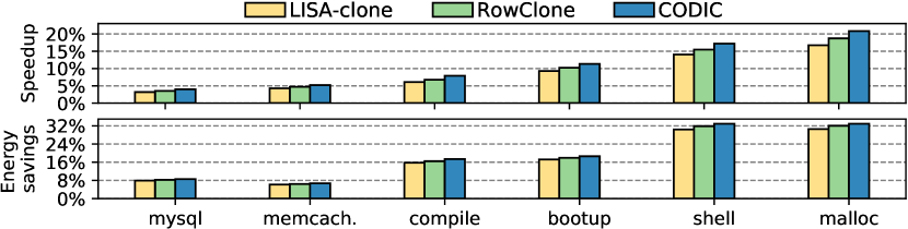
We make two observations. First, hardware approaches (LISA-clone, RowClone, CODIC) improve performance by up to 21% and energy savings by up to 34%, compared to the baseline software approach. Second, CODIC performs better and consumes less energy than LISA-clone and RowClone for all workloads.
Figure 9 shows the speedup and energy savings of CODIC and other state-of-the-art mechanisms in a 4-core processor, normalized to the performance and energy consumption of the software secure deallocation implementation.
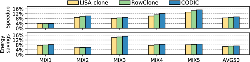
We make the same two observations as for a single core processor: 1) hardware approaches perform better than the software approach, and 2) CODIC performs better than LISA-clone and RowClone.
We have demonstrated the flexibility of the CODIC substrate with our secure deallocation mechanism, in addition to a better DRAM PUF (Section 5.1) and an efficient cold boot attack prevention mechanism (Section 5.2). Our evaluation shows that our CODIC-based secure deallocation mechanism has higher performance and energy efficiency compared to the state-of-the-art. We conclude that in addition to being flexible, CODIC is a very powerful substrate that enables more secure and efficient security mechanisms.
Appendix B NIST Test Suite Results
Table 10 shows the average NIST [123] p-values and NIST final results for signatures generated by CODIC-sig from different challenges.
| NIST Test | p-value | Result |
| monobit | 0.681 | PASS |
| frequency_within_block | 1.000 | PASS |
| runs | 0.298 | PASS |
| longest_run_ones_in_a_block | 0.287 | PASS |
| binary_matrix_rank | 0.536 | PASS |
| dft | 0.165 | PASS |
| non_overlapping_template_matching | 0.808 | PASS |
| overlapping_template_matching | 0.210 | PASS |
| maurers_universal | 0.987 | PASS |
| linear_complexity | 0.0185 | PASS |
| serial | 0.988 | PASS |
| approximate_entropy | 0.194 | PASS |
| cumulative_sums | 0.940 | PASS |
| random_excursion | 0.951 | PASS |
| random_excursion_variant | 0.693 | PASS |
Our results show that the values generated by CODIC-sig pass all 15 NIST randomness tests, which demonstrates that our PUF is able to return high-quality random signatures for different challenges.
Appendix C CODIC-sigsa
This section describes CODIC-sigsa, an alternative CODIC variant for generating signature values. CODIC-sigsa generates signature values by sensing and amplifying a precharged bitline that is not connected to the DRAM cell (i.e., the wordline is not raised). By doing so, the SA amplifies the bitline voltage to a signature value that 1) does not depend on the charge level of any cell, and 2) depends only on the SA process variation present in the SA and the bitline. Once the SA drives the bitline towards the final restored value, CODIC-sigsa can optionally write this value into a cell by raising the wordline.
Figure 10 shows the SPICE simulation of CODIC-sigsa. CODIC-sigsa raises the sense_p and sense_n signals (at 3ns) before it raises the wl signal (at 5ns). Because the bitline is initially precharged to voltage, the SA (sense_n and sense_p) amplifies the sensed value of the bitline to zero or one depending purely on process variation (in this example, the SA amplifies the bitline value to zero).
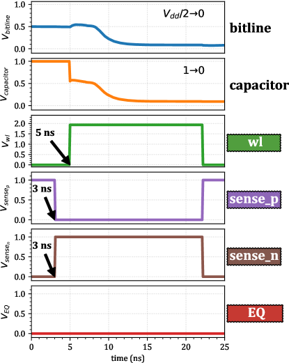
Evaluation Methodology. We evaluate CODIC-sigsa as a PUF with SPICE simulations. Unfortunately, it is infeasible to conduct experiments on real DRAM chips, as CODIC-sigsa requires changes to the internal DRAM timings, which are hard-wired in commodity DRAM chips. To show the effects of process variation on the values generated by CODIC-sigsa, we evaluate a detailed SA SPICE model (see Section 4.3) using Monte Carlo simulations. We model variations in all the affected components of the SAs (transistor length/width/threshold voltage). Our SA model always generates ‘1’ values in absence of process variation. When we introduce process variation into the simulation, we observe that some SAs generate ‘0’ values as well (i.e., some SAs generate bit flips). We run 100,000 simulations for each variation.
Evaluation Results. Table 11 shows the percentage of SAs that generate bit flips with CODIC-sigsa. The positions of the SAs that cause bit flips with CODIC-sigsa are random, and depend on process variation. We perform simulations for different levels of process variation and temperature.
| PV effects | Temperature effects (4% PV) | |||||||
| 2% | 3% | 4% | 5% | 30∘C | 60∘C | 70∘C | 85∘C | |
| Bit flips | 0.00% | 0.00% | 0.02% | 0.19% | 0.02% | 0.19% | 0.21% | 0.15% |
We make three main observations. First, small process variation amounts (4%) are not enough to generate CODIC-sigsa bit flips. Second, large process variation amounts increase the number of SAs that generate bit flips with CODIC-sigsa. As the technology scales, process variation becomes more significant, which increases the number of bit flips generated by CODIC-sigsa. Third, temperature changes do not cause significant variations in the number of SAs that cause bit flips with CODIC-sigsa.
Appendix D Evaluated DRAM Chips
| Module | Vendor | Chips | Pins | Ranks | Chip size (Gb) | Freq. (MT/s) | Voltage |
| A | 8 | 8 | 1 | 4 | 1600 | 1.35V (DDR3L) | |
| A | 8 | 8 | 1 | 4 | 1600 | 1.35V (DDR3L) | |
| A | 8 | 8 | 1 | 4 | 1600 | 1.35V (DDR3L) | |
| A | 8 | 8 | 1 | 4 | 1600 | 1.35V (DDR3L) | |
| A | 8 | 8 | 1 | 4 | 1600 | 1.50V (DDR3) | |
| A | 8 | 8 | 1 | 4 | 1600 | 1.50V (DDR3) | |
| A | 8 | 8 | 1 | 4 | 1600 | 1.50V (DDR3) | |
| A | 8 | 8 | 1 | 4 | 1600 | 1.50V (DDR3) | |
| B | 16 | 8 | 2 | 2 | 1333 | 1.50V (DDR3) | |
| B | 16 | 8 | 2 | 2 | 1333 | 1.50V (DDR3) | |
| B | 8 | 8 | 1 | 4 | 1600 | 1.35V (DDR3L) | |
| C | 8 | 8 | 1 | 4 | 1600 | 1.35V (DDR3L) | |
| C | 8 | 8 | 1 | 4 | 1600 | 1.35V (DDR3L) | |
| C | 8 | 8 | 1 | 4 | 1600 | 1.35V (DDR3L) | |
| C | 8 | 8 | 1 | 4 | 1600 | 1.35V (DDR3L) |