Probing charge dynamics in diamond with an individual color center
Abstract
Control over the charge states of color centers in solids is necessary in order to fully utilize them in quantum technologies. However, the microscopic charge dynamics of deep defects in wide-bandgap semiconductors are complex, and much remains unknown. Here, we utilize single shot charge state readout of an individual nitrogen-vacancy (NV) center to probe charge dynamics of the surrounding defects in diamond. We show that the NV center charge state can be converted through the capture of holes produced by optical illumination of defects many microns away. With this method, we study the optical charge conversion of silicon-vacancy (SiV) centers and provide evidence that the dark state of the SiV center under optical illumination is SiV2-. These measurements illustrate that charge carrier generation, transport, and capture are important considerations in the design and implementation of quantum devices with color centers, and provide a novel way to probe and control charge dynamics in diamond.
keywords:
nitrogen-vacancy centers, silicon-vacancy centers, charge dynamics, charge carrier transport, charge conversion, charge carrier capture, diamond, quantum sensingCentro de Investigación en Nanotecnología y Materiales Avanzados, Pontificia Universidad Católica de Chile, Santiago, Chile
Defects in diamond such as nitrogen-vacancy (NV) 1 and silicon-vacancy (SiV) 2 centers have emerged as promising quantum science platforms 3, 4, 5, 6, 7, 8, 9. However, control over the charge states of color centers is critical to realizing many applications. As a result, techniques for preparing color center charge states are actively being explored 10, 11, 12, 13, 14, 15, 16, but much remains unclear, and to date experiments have primarily focused on the charge state of individual centers. A deeper understanding of the dynamics of charge carriers in diamond is required in order to move beyond isolated color centers to arrays 6, 8, 17.
In this work, we use an individual NV center to study charge dynamics in diamond. These dynamics include optically changing a defect’s charge state through the photogeneration of free charge carriers from that defect, as well as the transport and capture of these charge carriers by other defects. We define the photogeneration of holes as the optical release of holes from a defect state to the valence band via photoexcitation of electrons from the valence band to the defect. Alternatively, the photogeneration of electrons refers to the photoexcitation of an electron from the defect state into the conduction band. In prior works, the average charge state of ensembles of NV centers in diamond has been observed to change due to the capture of charge carriers generated by optical illumination of defects several microns away 18, 19, 20, 21. However, the same ensemble of NV centers was used to both produce and capture the charge carriers, leading to a complex interplay of the processes involved. Our use of single-shot charge state readout of an isolated NV center to probe the capture of holes produced by hole photogeneration of a different defect species allows us to isolate the different processes. We use this method (Fig.1(a)) to investigate the charge dynamics of ensembles of SiV centers and observe exchange of charge carriers between SiV centers and a single NV center. Furthermore, while SiV- centers are known to enter a dark state under optical illumination 19, 22, the charge of this dark state is still debated 22, alternatively being assigned to SiV0 19, 23, 24 or SiV2- 25, 26. The mechanism by which a specific SiV center is returned to the SiV- charge state is also not understood. Our measurements present clear evidence that illumination of an SiV center in the SiV- charge state with 515 nm, 589 nm, or 638 nm light results in hole generation and conversion to the optically dark and spin-less SiV2- state, while illumination of other nearby defects can be used to return it to the SiV- state via hole capture. This new measurement technique provides a unique probe of the microscopic charge dynamics in diamond and a novel tool for realizing new levels of charge control over individual defects.

Experiments were conducted under ambient conditions using a home-built confocal microscope, with a 1.3 NA oil immersion objective. The laser focus was positioned at x and y using scanning galvanometer mirrors and a 4- lens configuration. The focus was fixed at 30 µm below the diamond surface to mitigate surface effects.
Two as-grown chemical-vapor deposition bulk diamond samples were used in our experiments. Sample A, from Diamond Elements, has an NV center concentration of ppb, as well as a high concentration of SiV centers. The density of native NV centers is low enough to resolve and address them individually. The concentration of SiV centers in Sample A was not measured directly, but is at least 10 ppb, as individual SiV defects are not optically resolvable. Sample B, from Element Six, has an NV center concentration of ppb, with no detectable concentration of SiV centers. The N defect concentrations of Sample A and B are assumed to be roughly ppb and ppb, respectively, based on the native NV concentration 27. Figure 1(b) shows the fluorescence spectrum of the NV- (i) and SiV- (ii) charge states. The separation in wavelength of the NV- and SiV- emission enables spectral filtering to isolate either the NV- or SiV- fluorescence as depicted by the respective blue and red band in Fig. 2(b).
In order to study defect charge conversion and the photogeneration, transport, and capture of charge carriers in diamond we introduce a new technique that makes use of charge-state readout of a single NV center, which we call “Spatial Photogeneration and Capture of chargE” (SPaCE). The experimental sequence is illustrated in Fig. 1(a). First, a single spatially resolved NV center at position (0, 0) (see Fig. 1(c)) is prepared by an “initialization” pulse. In the pulse sequence shown here, the initialization laser pulse is 515 nm (green), which prepares the NV in the NV- charge state with probability 28, 10. The microscope focus is moved to a new spot (xi, yi) in the confocal plane (at the same depth below the diamond surface) and a “charge photogeneration ” (CPG) pulse is applied for time . The defects at this location may photogenerate holes and electrons, which travel out into the diamond and can be captured by the NV center, altering its charge state. Finally, a low power 589 nm (yellow) “readout” laser pulse is used to measure the resulting charge state of the NV at (0,0) 29 (see Supplemental Materials for more details 28). This sequence is repeated for different (xi, yi) positions of the CPG pulse and the entire measurement sequence is repeated multiple times to produce a spatial map of the average charge state probability of the NV center as a function of CPG pulse location.
Figure 1(d) shows the outcome of SPaCE experiments performed on Sample A and Sample B, measured on the respective single NV centers circled in (c). There are three distinctive features in the measurement from Sample A. First, the bright region in the center corresponds to the CPG pulse directly illuminating the NV center, leaving it in the NV- state with a probability. The size of this central region is related to the CPG pulse beam waist, duration, and intensity. Second, there is a bright area around the edges of the plot corresponding to CPG pulses positioned at radial distances greater than 5 microns from the NV center, which for the 5 ms pulse duration shown here leaves the NV center charge state unaffected.
Lastly there is a dark ring centered on (0,0) microns, which corresponds to application of the CPG pulse at a radial distance between 1 µm and 5 µm from the NV center. With the 5 ms CPG pulse positioned within this range, the NV center had a high probability to be converted from NV- to NV0 at some point during the pulse.
For comparison, the same SPaCE measurement on an NV center in Sample B does not produce a dark ring, even at longer CPG pulse times (up to 100 ms). This implies the NV0 ring’s presence in Sample A and absence in Sample B is due to a difference between the two samples (the same behaviors were also observed with many other NVs in both samples). While there are differences in NV center and N defect concentrations between the two samples, we argue that these differences cannot account for the observations. A comparison of Sample B’s confocal scan in Fig. 1(c) and its SPaCE measurement in Fig. 1(d) (which represent the same spatial area) reveals that the central NV center remains bright when the CPG pulse is positioned over other nearby NV centers. We conclude that for the pulse durations, powers, and defect densities used in this work, charge carriers generated by illumination of surrounding isolated NV centers do not play a role in the observed charge dynamics. Furthermore, substitutional N defects do not produce holes under 515 nm illumination 30, 18, 19. While 515 nm illumination can photoionize N0 to N+, releasing electrons into the conduction band, this cannot explain the conversion of NV- to NV0. We therefore attribute the dark ring observed in the SPaCE measurements in Sample A to charge capture of holes released into the valence band by optical charge conversion of SiV centers during the CPG pulse, which we know to be present in Sample A and not in Sample B.

The attribution of the charge state conversion to holes photogenerated by charge conversion of SiV centers can be confirmed by taking advantage of the resolved defect spectra shown in Fig. 1(b). The outcome of identical SPaCE measurement sequences for an NV center and an ensemble of SiV centers are shown in the left and right column of Fig. 2(a), respectively, for varying CPG pulse lengths, (see Supplemental Materials for additional measurements 28). As opposed to the single NV center measurements, the density of the SiV defects is too high to isolate individual SiV centers and their concentration can only be estimated, so a single-shot charge state probability cannot be assigned to the SiV centers. Instead, these measurements extract the relative SiV- fluorescence following the SPaCE sequence from an ensemble of readout SiVs at the center (spatial position (0,0) microns, same as the NV center), with the number of SiV centers contributing to the measurement determined by the confocal volume and the local SiV density.
As shown in Fig. 2(a), SPaCE measurements performed with readout in the SiV spectral band exhibit similar but inverted features relative to the NV SPaCE measurements. The dark region in the center, which corresponds to applying the CPG pulse directly to the central readout SiV centers, indicates that a millisecond (or longer) 515 nm laser pulse converts SiV centers to a dark state, consistent with prior reports 19. When the laser is pulsed at larger radial distances around the edges of the plots, the fluorescence from the central SiV centers is also low. This corresponds to the SiV charge state after the previous measurement and initialization pulse, which together prepare them mainly in the dark state. Finally, in contrast to the dark ring in the NV measurements, the SiV centers exhibit a bright ring, which corresponds to the CPG pulse positioned a few microns away causing the central readout SiV centers to convert from their dark state to the bright SiV- charge state. This strongly suggests that just as the NV center captures holes, the SiV centers also capture holes photogenerated by charge conversion of surrounding SiV centers, resulting in the bright ring. Based on the combined observations that direct illumination with green light converts the SiV center into the dark state, the conversion of NV- to NV0 during SiV photo-conversion, and the strong anti-correlation between NV and SiV charge states, we conclude that the observed SiV dark state must be SiV2-. This is further supported by the lack of any fluorescence signal from SiV0 in this sample (see Supplemental Material 28).
Figure 2(b) shows the radial averages 28 of the SPaCE measurements as a function of distance from the center. The data is well described by the difference of two Gaussian functions:
| (1) |
where and are fit parameters and are allowed to vary for different CPG pulse times, . The two Gaussian functions in Eq. 1 correspond to two competing processes: capture of free holes and direct photoconversion by the laser. For the NV measurements the width of the negative Gaussian, , corresponds to the hole capture process. This parameter is extracted from the NV data fits as a function of (see Supplemental Material for additional measurements and details 28), and is shown in Figure 2(c). For CPG pulse times less than or equal to 25 ms, is well described by , where µm2/ms is an effective hole diffusion constant in the presence of SiV centers and N defects for the sample and laser power used here.
In order to better understand the origin of the effective diffusion constant, we applied a model following Refs. 19 and 21 that consists of a system of equations describing the diffusion of photogenerated charge carriers (holes and electrons) and dynamics of carrier capture by the defects present in the sample (N0/N+, NV-/NV0, SiV2-/SiV-; see Fig. 2(d) and Supplemental Materials 28). Using the cylindrical symmetry approximation employed in Refs. 19 and 21, we could not obtain a good simultaneous fit to all the experimental radially-averaged SPaCE data using a single set of adjustable parameters, even though the model could qualitatively reproduce the shape of the data (see the Supplemental Material 28). Our analysis found the simulations strongly depend on the SiV2- hole capture rate, which varied over an order of magnitude between fits of different CPG pulse times. We conjecture that the failure of this model to quantitatively reproduce the data with a single set of free rate parameters suggests that the effective diffusion constant arises in part from charge dynamics taking place outside of the focal plane, which are not captured by the cylindrically symmetric model. We leave simulations in three dimensions for future work.
Figure 2(d) depicts the three relevant charge carrier capture and charge carrier photogeneration processes observed in this work. Hole photogeneration through defect charge state conversion can occur for NV centers (NV0 to NV-) under illumination with 515 nm light 28, 10, 15 and for SiV centers (SiV- to SiV2-) under illumination with both 515 nm light and 638 nm light (see Supplemental Materials 28). Electron release through the photoionization of NV- to NV0 occurs under 515 nm light (at a slower rate than the opposite process) and 638 nm light, but does not occur for the SiV center for optical wavelengths. Finally, we find that both NV and SiV centers capture free holes (black arrows), but do not capture free electrons at significant rates. Hole capture is therefore the only way to convert from SiV2- to SiV- based on our observations, although photoionization of SiV2- may be possible with UV wavelengths 26. This indicates that in applications involving individual SiV- centers 9, returning to the SiV- charge state from the dark state can be accomplished by shining 515 nm light on other nearby defects, and not necessarily on the SiV center itself.
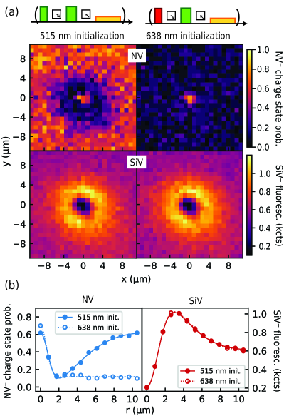
In Fig. 3(a), SPaCE measurements are shown with a 638 nm (red) initialization pulse which prepares the central NV in the NV0 state 15 (top right), in contrast to the 515 nm initialization pulse used in Figs. 1 and 2 that prepare the central NV center predominantly in the NV- state (top left). For 638 nm initialization, only a bright central region is observed. This corresponds to the CPG pulse directly illuminating the central NV center and directly converting to NV- from the NV0 state. The fact that outside this region the NV center remains in the NV0 state indicates that on these time scales the NV center does not capture electrons generated from other photoionized defects, such as N defects. This is in agreement with previous reports that the NV0 electron-capture cross-section is consistent with zero 19. Also shown are the measurements using the SiV spectral band for 638 nm initialization (bottom plots of Fig. 3(a) and right plot of (b)). The SiV charge state dynamics are unchanged by the wavelength of the initialization pulse.

To demonstrate that the impacts of charge capture can be mitigated by control over the surrounding charge environment, SPaCE measurements were performed after preparing the surrounding SiV centers in a specific charge state before each initialization pulse. As shown in Fig. 4(a), the measurement area was raster scanned to prepare a majority of the SiV centers in either the SiV- or SiV2- charge state following the protocol developed in Ref. 19. Confocal scans over the same area as the SPaCE measurements show a homogeneous SiV charge state after the raster scan, with the count rate in the SiV band after SiV- preparation approximately double those after SiV2- preparation.
The corresponding SPaCE measurements performed on the NV center are shown in Fig. 4(a). The two measurement sequences are identical, with the only difference between the two data sets being the SiV center preparation raster scans performed prior to each SPaCE measurement sequence. As the initialization pulse is applied after the raster scan, the NV center charge state is not affected by the SiV center preparation, but the subsequent charge dynamics are. When the surrounding SiV centers are prepared primarily in the SiV2- charge state (right), the probability that an NV captures a hole and is converted to NV0 is reduced significantly compared to when the surrounding SiV centers are prepared in the SiV- charge state (left). Figure 4(b) shows the radial averages of the measurements in (a), along with fits to Eq. 1. The width of the charge capture Gaussian curve, 28 , was reduced by a factor of 1.6 by preparing the surrounding SiV centers in the SiV2- state.
In conclusion, we have presented a new measurement technique that makes use of single NV centers to probe photogeneration of holes from surrounding defects, hole transport, and hole capture. Using this technique, hole exchange between SiV centers and a single NV center over micron distances was observed. These observations show that the dark state of the SiV center under optical illumination is the SiV2- charge state, and that the primary mechanism for its return to the bright SiV- state is through charge capture of holes photogenerated by charge conversion of other surrounding defects. We have also demonstrated that the impact of hole capture on a single NV center can be partially mitigated by engineering the surrounding defect charge state environment. The SPaCE measurement technique demonstrated here can be readily applied to any diamond sample containing spatially resolved NV centers, and is adaptable to any color center where the charge state can be optically measured, enabling the future study of the charge dynamics of a broad range of defects. Finally, the observation of charge conversion of single NV centers due to charge exchange with defects many microns away highlights the importance of considering charge dynamics in experiments with arrays of color centers, and points the way to new methods of color center charge state engineering and control.
Author’s note: During preparation of this manuscript we became aware of complementary work in which charge transport and capture between two individual nitrogen vacancy centers in diamond was observed 31, 32.
1 Acknowledgements
The authors thank Nathalie de Leon for enlightening discussions, helpful insights, and comments on the manuscript. Experimental work, data analysis, and theoretical efforts conducted at UW–Madison and Lawrence Livermore National Laboratory were supported by the U.S. Department of Energy (DOE), Office of Science, Basic Energy Sciences (BES) under Award #DE-SC0020313. Part of this work by V.L. was performed under the auspices of the U.S. Department of Energy at Lawrence Livermore National Laboratory under Contract DE-AC52-07NA27344. Theoretical contributions conducted at Pontificia Universidad Católica de Chile by J. R. M. and A. N. were supported by ANID Fondecyt 1180673 and ANID PIA ACT192023. A. N. and H. T. D. acknowledge financial support from Universidad Mayor through the Postdoctoral Fellowship. A. G. acknowledges support from the Department of Defense through the National Defense Science and Engineering Graduate Fellowship (NDSEG) program.
References
- Doherty et al. 2013 Doherty, M. W.; Manson, N. B.; Delaney, P.; Jelezko, F.; Wrachtrup, J.; Hollenberg, L. C. The nitrogen-vacancy colour centre in diamond. Physics Reports 2013, 528, 1–45
- Müller et al. 2014 Müller, T.; Hepp, C.; Pingault, B.; Neu, E.; Gsell, S.; Schreck, M.; Sternschulte, H.; Steinmüller-Nethl, D.; Becher, C.; Atatüre, M. Optical signatures of silicon-vacancy spins in diamond. Nat. Commun. 2014, 5
- Rondin et al. 2014 others,, et al. Magnetometry with nitrogen-vacancy defects in diamond. Rep. Prog. Phys. 2014, 77, 056503
- Dolde et al. 2011 others,, et al. Electric-field sensing using single diamond spins. Nat. Phys. 2011, 7, 459–463
- Togan et al. 2010 Togan, E.; Chu, Y.; Trifonov, A. S.; Jiang, L.; Maze, J.; Childress, L.; Dutt, M. V. G.; Sørensen, A. S.; Hemmer, P. R.; Zibrov, A. S.; Lukin, M. D. Quantum entanglement between an optical photon and a solid-state spin qubit. Nature 2010, 466
- Dolde et al. 2014 Dolde, F.; Bergholm, V.; Wang, Y.; Jakobi, I.; Naydenov, B.; Pezzagna, S.; Meijer, J.; Jelezko, F.; Neumann, P.; Schulte-Herbrüggen, T.; Biamonte, J.; Wrachtrup, J. High-fidelity spin entanglement using optimal control. Nat. Commun. 2014, 5
- Evans et al. 2018 Evans, R. E.; Bhaskar, M. K.; Sukachev, D. D.; Nguyen, C. T.; Sipahigil, A.; Burek, M. J.; Machielse, B.; Zhang, G. H.; Zibrov, A. S.; Bielejec, E.; Park, H.; Lončar, M.; Lukin, M. D. Photon-mediated interactions between quantum emitters in a diamond nanocavity. Science 2018, 362, 662–665
- Bradley et al. 2019 Bradley, C. E.; Randall, J.; Abobeih, M. H.; Berrevoets, R. C.; Degen, M. J.; Bakker, M. A.; Markham, M.; Twitchen, D. J.; Taminiau, T. H. A Ten-Qubit Solid-State Spin Register with Quantum Memory up to One Minute. Phys. Rev. X 2019, 9, 031045
- Bhaskar et al. 2020 Bhaskar, M. K.; Riedinger, R.; Machielse, B.; Levonian, D. S.; Nguyen, C. T.; Knall, E. N.; Park, H.; Englund, D.; Lončar, M.; Sukachev, D. D.; Lukin, M. D. Experimental demonstration of memory-enhanced quantum communication. Nature 2020, 580
- Waldherr et al. 2011 Waldherr, G.; Beck, J.; Steiner, M.; Neumann, P.; Gali, A.; Frauenheim, T.; Jelezko, F.; Wrachtrup, J. Dark States of Single Nitrogen-Vacancy Centers in Diamond Unraveled by Single Shot NMR. Phys. Rev. Lett. 2011, 106, 157601
- Grotz et al. 2012 Grotz, B.; Hauf, M.; Dankerl, M. V.; Naydenov, B.; Pezzagna, S.; Meijer, J.; Jelezko, F.; Wrachtrup, J.; Stutzmann, M.; Reinhard, F.; Garrido, J. A. Charge state manipulation of qubits in diamond. Nat. Commun. 2012, 5
- Fu et al. 2010 Fu, K.-M. C.; Santori, C.; Barclay, P. E.; Beausoleil, R. G. Conversion of neutral nitrogen-vacancy centers to negatively charged nitrogen-vacancy centers through selective oxidation. Applied Physics Letters 2010, 96, 121907
- Hauf et al. 2011 Hauf, M. V.; Grotz, B.; Naydenov, B.; Dankerl, M.; Pezzagna, S.; Meijer, J.; Jelezko, F.; Wrachtrup, J.; Stutzmann, M.; Reinhard, F.; Garrido, J. A. Chemical control of the charge state of nitrogen-vacancy centers in diamond. Phys. Rev. B 2011, 83, 081304
- Rose et al. 2018 Rose, B. C.; Huang, D.; Zhang, Z.-H.; Stevenson, P.; Tyryshkin, A. M.; Sangtawesin, S.; Srinivasan, S.; Loudin, L.; Markham, M. L.; Edmonds, A. M.; Twitchen, D. J.; Lyon, S. A.; de Leon, N. P. Observation of an environmentally insensitive solid-state spin defect in diamond. Science 2018, 361, 60–63
- Aslam et al. 2013 Aslam, N.; Waldherr, G.; Neumann, P.; Jelezko, F.; Wrachtrup, J. Photo-induced ionization dynamics of the nitrogen vacancy defect in diamond investigated by single-shot charge state detection. New Journal of Physics 2013, 15, 013064
- Irber et al. 2021 Irber, D. M.; Poggiali, F.; Kong, F.; Kieschnick, M.; Lühmann, T.; Kwiatkowski, D.; Meijer, J.; Du, J.; Shi, F.; Reinhard, F. Robust all-optical single-shot readout of nitrogen-vacancy centers in diamond. Nat. Commun. 2021, 12
- Oberg et al. 2019 Oberg, L. M.; Huang, E.; Reddy, P. M.; Alkauskas, A.; Greentree, A. D.; Cole, J. H.; Manson, N. B.; Meriles, C. A.; Doherty, M. W. Spin coherent quantum transport of electrons between defects in diamond. Nanophotonics 2019, 8, 1975–1984
- Jayakumar et al. 2016 Jayakumar, H.; Henshaw, J.; Dhomkar, S.; Pagliero, D.; Laraoui, A.; Manson, N.; A,; Doherty, M.; Meriles, C. Optical patterning of trapped charge in nitrogen-doped diamond. Nat. Commun. 2016, 7
- Dhomkar et al. 2018 Dhomkar, S.; Zangara, P. R.; Henshaw, J.; Meriles, C. A. On-Demand Generation of Neutral and Negatively Charged Silicon-Vacancy Centers in Diamond. Phys. Rev. Lett. 2018, 120, 117401
- Lozovoi et al. 2020 Lozovoi, A.; Daw, D.; Jayakumar, H.; Meriles, C. A. Dark defect charge dynamics in bulk chemical-vapor-deposition-grown diamonds probed via nitrogen vacancy centers. Phys. Rev. Materials 2020, 4, 053602
- Jayakumar et al. 2020 Jayakumar, H.; Lozovoi, A.; Daw, D.; Meriles, C. A. Long-Term Spin State Storage Using Ancilla Charge Memories. Phys. Rev. Lett. 2020, 125, 236601
- Nicolas et al. 2019 Nicolas, L.; Delord, T.; Huillery, P.; Pellet-Mary, C.; Hétet, G. Sub-GHz Linewidth Ensembles of SiV Centers in a Diamond Nanopyramid Revealed by Charge State Conversion. ACS Photonics 2019, 6, 2413–2420
- D’Haenens-Johansson et al. 2011 D’Haenens-Johansson, U. F. S.; Edmonds, A. M.; Green, B. L.; Newton, M. E.; Davies, G.; Martineau, P. M.; Khan, R. U. A.; Twitchen, D. J. Optical properties of the neutral silicon split-vacancy center in diamond. Phys. Rev. B 2011, 84, 245208
- Green et al. 2019 Green, B. L.; Doherty, M. W.; Nako, E.; Manson, N. B.; D’Haenens-Johansson, U. F. S.; Williams, S. D.; Twitchen, D. J.; Newton, M. E. Electronic structure of the neutral silicon-vacancy center in diamond. Phys. Rev. B 2019, 99, 161112
- Gali and Maze 2013 Gali, A.; Maze, J. R. Ab initio study of the split silicon-vacancy defect in diamond: Electronic structure and related properties. Phys. Rev. B 2013, 88, 235205
- Breeze et al. 2020 Breeze, B. G. et al. Doubly charged silicon vacancy center, Si-N complexes, and photochromism in N and Si codoped diamond. Phys. Rev. B 2020, 101, 184115
- Edmonds et al. 2012 Edmonds, A. M.; D’Haenens-Johansson, U. F. S.; Cruddace, R. J.; Newton, M. E.; Fu, K.-M. C.; Santori, C.; Beausoleil, R. G.; Twitchen, D. J.; Markham, M. L. Production of oriented nitrogen-vacancy color centers in synthetic diamond. Phys. Rev. B 2012, 86, 035201
- 28 See Supplemental Material for experimental details, additional data, and theoretical details.
- Shields et al. 2015 Shields, B. J.; Unterreithmeier, Q. P.; de Leon, N. P.; Park, H.; Lukin, M. D. Efficient Readout of a Single Spin State in Diamond via Spin-to-Charge Conversion. Phys. Rev. Lett. 2015, 114, 136402
- Isberg et al. 2006 Isberg, J.; Tajani, A.; Twitchen, D. J. Photoionization measurement of deep defects in single-crystalline CVD diamond using the transient-current technique. Phys. Rev. B 2006, 73, 245207
- Lozovoi et al. 2021 Lozovoi, A.; Daw, D.; Vizkelethy, G.; Bielejec, E.; Jayakumar, H.; Meriles, C. Transport of photogenerated carriers between individual NV centers in diamond. Proceedings of APS March Meeting. 2021
- Lozovoi et al. 2021 Lozovoi, A.; Jayakumar, H.; Daw, D.; Vizkelethy, G.; Bielejec, E.; Flick, J.; Doherty, M.; Meriles, C. Optical activation and detection of charge transport between individual color centers in room-temperature diamond. Submitted 2021,