Imaging spin-wave damping underneath metals using electron spins in diamond
1 Department of Quantum Nanoscience, Kavli Institute of Nanoscience, Delft University of Technology, Lorentzweg 1, 2628 CJ, Delft, The Netherlands
2 Huygens - Kamerlingh Onnes Laboratorium, Leiden University, Niels Bohrweg 2, 2300 RA, Leiden, The Netherlands
3 Max Planck Institute for the Structure and Dynamics of Matter, Luruper Chausee 149, 22761 Hamburg, Germany
4 WPI-AIMR & Institute for Materials Research & CSRN, Tohoku University, Sendai 980-8577, Japan
∗ Corresponding author. Email: T.vanderSar@tudelft.nl.
Abstract
Spin waves in magnetic insulators are low-damping signal carriers that could enable a new generation of spintronic devices. The excitation, control, and detection of spin waves by metal electrodes is crucial for interfacing these devices to electrical circuits. It is therefore important to understand metal-induced damping of spin-wave transport, but characterizing this process requires access to the underlying magnetic films. Here we show that spins in diamond enable imaging of spin waves that propagate underneath metals in magnetic insulators, and then use this capability to reveal a 100-fold increase in spin-wave damping. By analyzing spin-wave-induced currents in the metal, we derive an effective damping parameter that matches these observations well. We furthermore detect buried scattering centers, highlighting the technique’s power for assessing spintronic device quality. Our results open new avenues for studying metal - spin-wave interaction and provide access to interfacial processes such as spin-wave injection via the spin-Hall effect.
1 Main Text
Introduction
Spin waves are collective, wave-like excitations of the spins in magnetic materials[1]. The field of magnon spintronics aims at using these waves as signal carriers in information processing devices[2]. Since its recent inception, the field has matured rapidly[3] and successfully realized prototypical spin-wave devices that implement logical operations[4, 5, 6, 7, 8]. In such devices, the spin waves are typically excited inductively[4, 5, 6, 7, 8] or via spin-pumping based on the spin-Hall effect[9, 10], using electric currents in metal electrodes that are deposited on top of thin-film magnetic insulators. As such, it is a key challenge to understand the interaction between the metals and the spin waves in the magnetic insulators, but this requires the ability to study the buried magnetic films and is hampered by the opacity of the metals to optical probes.
We address this challenge using magnetic imaging based on electron spins in diamond[11]. Metal films of sub-skin-depth thickness are transparent for microwave magnetic fields, which enables imaging of spin waves traveling underneath the metals by detecting their magnetic stray fields. We demonstrate this ability by imaging spin waves that travel underneath 200-nm-thick metal electrodes in a thin film of the magnetic insulator yttrium iron garnet (YIG). We find that the spatial spin-wave profiles under the metals reveal a surprisingly strong metal-induced spin-wave damping. By introducing the spin-wave-induced currents in the metal self-consistently into the Landau-Lifshitz-Gilbert (LLG) equation, we derive an analytical expression for the spin wave damping that matches our experimental observations without free parameters. We demonstrate that this eddy-current-induced damping mechanism dominates up to a threshold frequency above which three-magnon scattering becomes allowed and increases damping further.
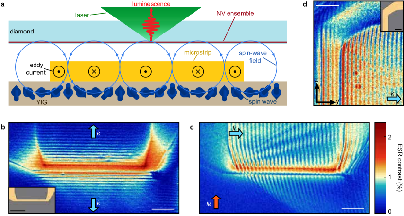
Our imaging platform is an ensemble of shallowly implanted nitrogen-vacancy (NV) centers in diamond (Fig. 1a). NV centers are lattice defects with an electron spin that can be polarized by optical excitation, controlled by microwaves, and read out through spin-dependent photoluminescence[12, 13]. Since NV centers can exist within nm from the surface of diamond[14], they can be brought within close proximity to a material of interest. Combined with an excellent sensitivity to magnetic fields[13], these properties make NV spins well suited for stray-field probing of spins and currents in condensed matter systems[15].
Results
To image propagating spin waves, we place a diamond membrane containing a layer of NV centers implanted nm below the diamond surface onto a YIG film equipped with 200 nm thick gold microstrips (Methods). Passing a microwave current through a microstrip generates a magnetic field that excites spin waves in the YIG (Fig. 1a). These waves create a magnetic stray field that interferes with the direct microstrip field, leading to a spatial standing-wave pattern in the total amplitude of the oscillating magnetic field[11]. We spatially map this amplitude by locally measuring the contrast of the NV electron spin resonance (ESR) transitions. By changing the drive frequency while adjusting the static magnetic field () to maintain resonance with the NV ESR frequency (Methods), we can excite and detect spin waves with wavevectors either along or perpendicular to the static magnetization (Fig. 1b-c). The spin waves are clearly visible both underneath and next to the gold microstrips (Fig. 1b-d).
To characterize the metal-induced spin-wave damping, we start by analyzing the spatial spin-wave profiles underneath and next to a gold microstrip that we use to excite spin waves (Fig. 2a). We select a section of microstrip that is far away from corners ( m) to avoid edge effects. We apply a static magnetic field with in-plane component along the microstrip direction and a drive frequency between 100-600 MHz above the ferromagnetic resonance (FMR), resulting in directional spin-wave emission with a large (small) spin-wave amplitude to the right (left) of the microstrip (Fig. 2a). This directionality is characteristic of microstrip-driven spin waves traveling perpendicularly to the magnetization and is a result of the handedness of the microstrip drive field and the precessional motion of the spins in the magnet[16, 17]. We spatially quantify the amplitude of the local microwave magnetic field generated by the spin waves by measuring the rotation rate (Rabi frequency) of the NV spins[18]. The spatial oscillations in the measured NV Rabi frequency result from the interference between the microstrip and spin-wave fields[11]. The spin-wavelength is directly visible from the spatial period of these oscillations. We observe a rapid decay of the oscillations underneath the microstrip (Fig. 2b), even though the microstrip field is approximately constant in this region (Fig. 2c). We can thus conclude that this decay is caused by the decay of the spin-wave amplitude. In contrast, the decrease of the amplitude away from the microstrip follows the decay of the direct microstrip field (Fig. 2c).
By fitting the measured spatial decay in- and outside the microstrip region we can extract the additional spin-wave damping caused by the metal (Supplementary Sections 3.1 and 3.2). An accurate description of the measured NV Rabi frequencies (Fig. 2a-c) is only possible if we allow for different damping constants in- and outside the microstrip region (see also Supplementary Figure 5). We find that the damping underneath the gold microstrip (Fig. 2d, red diamonds) exceeds the damping next to the microstrip (yellow squares) by approximately two orders of magnitude .
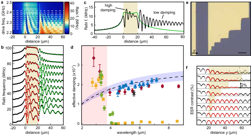
We argue that the observed strong spin-wave damping underneath the metal is caused by eddy currents that are induced by the oscillating magnetic stray field of the spin waves. Eddy currents have been reported to cause linewidth broadening of ferromagnetic resonances in cavity and stripline-based experiments[19, 20, 21, 22, 23, 24, 25]. However, revealing their effect on propagating spin waves, which is important for information transport, has remained an outstanding challenge. We model the effect of the spin-wave-induced currents by including their magnetic field self-consistently into the LLG equation (Supplementary Sections 3.1.4 and 3.1.5). Doing so, we find that a metal film of thickness increases the damping to , with the intrinsic ”Gilbert” damping and
| (1) |
with the electron gyromagnetic ratio, the vacuum permeability, and the YIG saturation magnetization and thickness, respectively, the spin-wavenumber, the metal resistivity, and the spin-wave ellipticity. This expression is derived under the assumption of a homogeneous magnetization across the film thickness , which becomes strictly valid in the thin-film limit . The form factor arises from spatially averaging the dipolar and eddy-current stray fields over the thicknesses of the YIG and metal films. An analysis equating the magnetic energy losses to the power dissipated in the metal yields the same expression (Supplementary Section 3.1.7). We plot Eq. 1 and its thin-film limit in Fig. 2d using m for the resistivity of gold[26], finding a good agreement with the damping extracted from the various sets of data without free parameters. The finite width of the stripline can be disregarded when (Supplementary Sections 3.1.6 and 3.1.7), as is the case in Fig. 2d. Accounting for a non-homogeneous magnetization may be achieved via micromagnetic simulations[16]
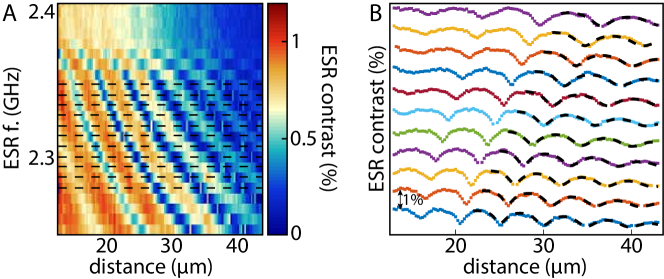
To corroborate the origin of the damping enhancement, we image spin waves propagating underneath a 200-nm-thick gold island deposited next to a microstrip (Fig. 2e-f). We observe a progressively decreasing spin-wave amplitude for increasing travel distance under the gold, with an average characteristic decay length of m extracted by fitting the top three traces in Fig. 2f. We characterize the wavelength dependence by varying the drive frequency (Supplementary Fig. 6). The corresponding damping values are reported in Fig. 2d (black cross and blue triangles) and agree well with Eq. 1.
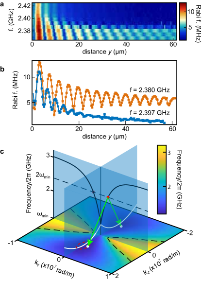
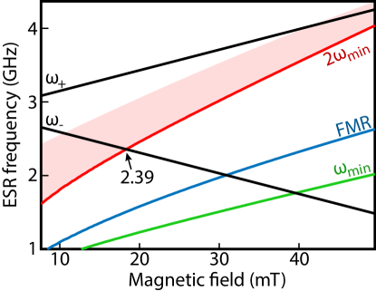
Both in- and outside the stripline region, we observe a sudden increase in damping above a threshold frequency GHz (Fig. 2a). We characterize this increase in detail by zooming in to the threshold frequency (Fig. 3a-b) and extracting the damping parameter as a function of the wavelength (Fig. 2d, green circles). For the spin waves outside the microstrip region, the increase occurs in a 10 MHz frequency range of the order of the intrinsic spin-wave linewidth.
By analyzing the known spin-wave dispersion of our YIG thin film (Supplementary Section 3.1.3), it becomes clear that the observed increase in damping above is a result of three-magnon scattering – a process in which one magnon decays into two of half the frequency and opposite wavevectors[27] (Fig. 3c): When the drive frequency is increased to above , three-magnon scattering becomes allowed because starts to exceed the bottom of the spin wave band () (Fig. 3c and Supplementary Fig. 7). The onset of three-magnon scattering was previously identified using Brillouin light scattering[28]. Our real-space imaging approach reveals its dramatic effect on the spatial spin-wave decay length important for spin-wave transport. These measurements highlight that damping caused by three-magnon scattering limits the frequency range within which coherent spin waves in YIG thin films can serve as low-damping carriers to .
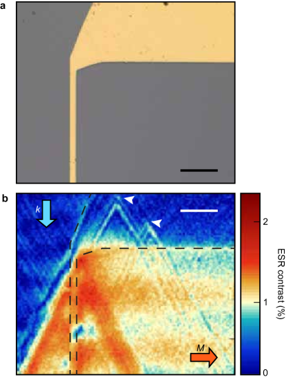
Finally, we demonstrate that the ability to study spin waves underneath metals also enables the detection of hidden spin-wave scattering centers, highlighting the applicability of this approach for assessing the quality of buried magnetic films in multilayer systems. As an example, we show the scattering patterns produced by defects underneath the metal electrodes used for spin-wave excitation (Fig. 4a-b). The defects produce characteristic v-shaped patterns, resulting from preferential scattering into the ”caustic” directions that are associated with the anisotropic dispersion[29], making the source of these spin-wave beams clearly identifiable. NV-based spin-wave imaging could therefore be used as a diagnostic tool for magnetic quality, even when the material of interest is buried under metallic layers in a heterostructure.
Discussion
In conclusion, we characterized the damping enhancement of spin waves that propagate under metallic electrodes used for spin-wave control, and showed that the increase is well explained by a model that introduces the spin-wave-induced currents into the LLG equation. The ability to detect spin waves underneath metals opens up several exciting new possibilities for studying the interaction between metals and magnets. One example is studying the spectral properties of temperature- or chemical-potential-driven magnon condensates underneath gates in magnon transistors[8, 30, 31]. Additionally, varying the thickness of the metal and/or magnetic films, or using spacer layers, enables a characterization of interfacial effects such as damping and anti-damping of magnons controlled by the spin-Hall effect in heavy metal electrodes. Furthermore, characterizing the screening of the spin-wave stray fields by a metal enables measuring its magnetic susceptibility at well-defined wavenumbers and extracting material parameters such as skin depth, conductivity and permeability. Finally, the ability to reveal buried scattering centers provides a new tool for assessing the quality of magnetic interfaces and spin-wave devices.
2 Materials and Methods
Sample fabrication
The diamond chip used in this work measured mm3 and had an estimated NV density of m2 created via ion implantation at a depth of 10-20 nm below the diamond surface (see fabrication details in[11]). The YIG film was 235 nm thick, grown on a 500 m-thick GGG substrate via liquid phase epitaxy (Matesy gmbh). The saturation magnetization was previously measured[11] to be A/m. To mount the NV-diamond, we deposit a drop of isopropanol onto the YIG and place the diamond on top with the NV-surface facing down, while gently pressing down until the IPA has evaporated. The resulting diamond-YIG distance is limited by small particles (e.g. dust). We extract an NV-YIG distance of 1.6(1) m from the measured maps of the NV Rabi oscillations.
NV-based imaging of spin waves
NV centers are optically addressed using a home-built confocal microscope with a 515 nm laser, an NA=0.95 objective for laser focusing/photon collection, and an avalanche photodiode for NV photon detection (for details of the setup, see[11]). The ESR transition of the NV centers used in this work for spin-wave imaging is tuned by a magnetic field according to where GHz/T is the electron gyromagnetic ratio and GHz is the zero-field splitting. In all experiments in Figs. 2-4, the magnetic field is oriented at a angle with respect to the sample-plane normal and with an in-plane projection along the microwave stripline, thus aligning it with one of the four possible crystallographic orientations of the NV centers in the diamond. The fields used in this work are below 25 mT, much smaller than the YIG saturation magnetization ( mT), therefore the YIG magnetization tilts out of plane by less than [11]. We measure Rabi oscillations by applying a s laser pulse to polarize the NV spin into the state, applying a microwave magnetic field at the NV ESR frequency, and reading out the final spin state through the NV’s spin-dependent photoluminescence[13].
Acknowledgements
Funding: This work was supported by the Dutch Research Council (NWO) as part of the Frontiers of Nanoscience (NanoFront) program through NWO Projectruimte grant 680.91.115.
Author contributions: I.B. and T.S. designed the experiment. B.S. prepared the diamond membrane. I.B. realized the NV magnetometry setup, fabricated the sample and performed the measurements. G.E.W.B., T.S, Y.M.B. and T.Y. developed the theoretical model. J.A. commented on the manuscript. I.B and T.S. analyzed the data and wrote the manuscript with help from all co-authors.
Data and materials availability: All data contained in the figures will be made available at 10.5281/zenodo.4726771 upon publication. Additional data related to this paper may be requested from the authors.
Competing interests: The authors declare no competing interest.
3 Supplementary Material
3.1 Eddy-current contribution to spin-wave damping
In this section we derive the additional spin-wave damping caused by the spin-wave-induced eddy currents in a nearby metallic layer. We use the Landau-Lifshitz-Gilbert (LLG) equation to evaluate the various components of the effective magnetic field and find solutions in the absence of additional damping. Then, we evaluate the spin-wave field inside the metal, derive the eddy currents excited by that field, and calculate the additional field component that acts back on the spin-waves, leading to an expression for the effective damping. Last, we consider the finite width of the metal film in the y direction and include this into the effective damping result.
We consider a thin film of a magnetic insulator (i.e. YIG) in the plane, between , with unit magnetization oriented along in equilibrium and saturation magnetization . The bias magnetic field is applied along . The system is translationally invariant along .
3.1.1 LLG equation
The LLG equation is [32]
| (2) |
where is the microstrip magnetic field, is the gyromagnetic ratio, is the Gilbert damping and the effective magnetic field is
| (3) |
where . We will now evaluate the various components of the effective magnetic field. We will assume that the spin-wavelength is much larger than the film thickness () such that we can approximate the magnetization to be homogeneous across the film thickness.
The free energy density includes contributions from the external field , the demagnetizing field , and the exchange interaction:
| (4) |
with the spin stiffness. We define, for convenience, , , and .
3.1.2 Evaluating the contributions to the effective magnetic field
Zeeman energy
The Zeeman energy associated with the external magnetic field is
| (5) |
Exchange energy
The exchange energy density in YIG is isotropic
| (6) |
Its Fourier transform over the in-plane coordinates is:
| (7) |
For a constant magnetization over the film thickness, the exchange energy contributes an effective field with Cartesian components:
| (8) |
Demagnetizing field
The magnetic field generated by a magnetization is given by [33]:
| (9) |
where is the real-space dipolar tensor, with components that are derivatives of the ”Coulomb kernel”:
| (10) |
The 2D Fourier transform of Eq. (9) is 111We define and :
| (11) |
where and with magnetization
| (12) |
The demagnetizing field, averaged over the film thickness, is given by:
| (13) |
where the overline indicates averaging over the thickness. The components of the dipolar tensor in Fourier space are:
| (14) |
Using
| (15) | |||
| (16) | |||
| (17) |
we arrive at
| (18) |
with for .
3.1.3 Spin-wave susceptibility
The linearized Eq. (2) in the frequency domain reads:
| (19) | ||||
| (20) |
Using and with (from Eq. (18)) we obtain
| (21) | ||||
| (22) | ||||
| (23) |
where is the angle between the wave vector and . With
| (24) | ||||
| (25) | ||||
| (26) |
we obtain Eqns. (19-20) in matrix form:
| (27) |
Inverting Eq. (27) gives the susceptibility
| (28) |
It is singular when:
| (29) |
The real parts of the solutions of this quadratic equation give the spin wave dispersion , plotted in Fig. 3c of the main text. In Fig. 3c, the solid lines indicate the dispersion for spin waves propagating along (i.e., and ) and along (i.e., ). The spin-wave linewidth follows from the imaginary part of Eq. (29), and the ellipticity of the magnetization precession is given by
| (30) |
Applying the bias field along as in the experiments changes , but does not introduce additional terms in the susceptibility for much smaller than the demagnetizing field (), as in this work.
3.1.4 Eddy-current-induced spin-wave damping
In this section, we introduce the field generated by eddy currents into the LLG equation. We first derive the eddy currents in a metal film (parallel to the plane and located between ) induced by the spin-wave stray field. The eddy currents in turn generate a magnetic field that couples back into the LLG equation, which should be solved self-consistently. We focus on spin waves travelling in the -direction, such that (thus ). Our films are much thinner than the magnetic skin depth ( m for gold at 2 GHz) such that the dipolar stray fields are not screened significantly. Because the film is thin, we neglect eddy currents in the out-of-plane direction. The in-plane eddy currents are induced by the out-of-plane component of the magnetic field, given by (see Eq. (LABEL:eq:FFT_Gamma)):
| (31) | ||||
| (32) |
where the overbar denotes an average over the metal () thickness. Here,
| (33) |
For an infinitely thin film, . From Faraday’s law, generates a charge current :
| (34) |
where is the conductivity and the electromotive force. As we will further discuss in 3.1.6, this equation is valid in the limit , with the width of the film, since we used a Fourier transform over and did not specify boundary conditions. In Fig. 2d of the main text, m and m, such that .
Field generated by the eddy currents
The current generates a field inside the YIG film. Its average over the YIG thickness is
| (35) | ||||
| (36) |
which we can rewrite as
| (37) | ||||
| (38) |
where
| (39) |
is a dimensionless factor that turns out to be the eddy current contribution to the damping as discussed in the next section. Because the equation was derived under the approximation of a homogeneous magnetization across the film thickness it is valid in the thin-film limit where . The factor arises from averaging the dipolar and eddy current stray fields over the thicknesses of the metal and magnet films. Including a non-homogeneous magnetization across the film thickness may be achieved via micromagnetic simulations. In Fig. 2d of the main text, (for m m.)
3.1.5 Solutions to the LLG equations with eddy currents
We now incorporate into the LLG equation by adding it to Eqs. (21-23) for
| (40) | ||||
| (41) | ||||
| (42) |
The linearized LLG equations (19-20) become
| (43) | ||||
| (44) |
where and are given in Eqs. (24-26). In matrix form:
| (45) |
The resulting susceptibility is singular when
| (46) |
Solving this quadratic equation and disregarding terms of order leads to
| (47) |
We observe that including the eddy currents yields the same spin-wave dispersion , but renormalizes the linewidth according to
| (48) |
where we assumed . The eddy-current-induced damping can thus be included into Eq. (2) by setting
| (49) |
Substituting Eq. (39) leads to Eq. 1 in the main text. In section 3.1.7 we find the same expression using an alternative derivation.
3.1.6 Metal film of finite width
We now consider a metal strip with finite width along . The effective orbital magnetization of the eddy currents induced by the spin-wave field points in the -direction and is determined by the Maxwell-Faraday equation:
| (50) |
where is the stray field of a spin wave travelling in the direction, Fourier transformed over time but not over coordinates. It is given by (c.f. Eq. (32))
| (51) |
Introducing the notations , the solution of Eq. (50) is
| (52) |
with
| (53) |
The eddy-current field averaged over the magnetic film thickness, cf. Eq. (35) is:
| (54) |
where
| (55) |
Note that it does not depend on . Using
| (56) |
from Eq. (55) we obtain
| (57) | ||||
| (58) |
and . In the wide-strip limit such that, back in the real-space and time domains,
| (59) |
The last term reflects that a spatially homogeneous mode does not induce eddy currents. The finite width can be neglected when , in which case we get the same result as Eq. (39). In Fig. 2d of the main text, .
3.1.7 Effective magnetic damping
The effective damping parameter can be derived alternatively by equating the magnetic and external energy losses [34]. According to the LLG equation the power density per area of a dynamic magnetization for a scalar Gilbert damping constant reads
| (60) |
where the integral is over the magnetic film thickness. In our geometry the power loss density of a spin wave mode with index that solves the linearized LLG with frequency is then
| (61) |
In the limit , we can replace by the wave number of the spin wave in the direction. The time ()-dependent magnetization
| (62) |
leads to the time-averaged dissipation
| (63) |
We model the energy loss per unit of length under the strip by a phenomenological damping parameter as
| (64) |
where the over-bar indicates the spatial average over the film thickness . Assuming that the magnetic skin depth is much larger than the thickness of the strip , the stray field averaged over the strip thickness above the film and reads
| (65) |
This field generates an electromotive force (emf) according to :
| (66) | ||||
| (67) |
The emf does not drive a net charge current since the metal strip is part of a high impedance circuit.
| (68) |
then fixes the integration constant The time-averaged () integrated Ohmic loss per unit length of the wire then reads
| (69) | ||||
| (70) |
We can now determine the effective damping by setting
| (71) |
In the long-wavelength and wide-metal-strip regime , and
| (72) |
agrees with Eq. (49). We note that the scalar should be interpreted as an appropriate average over the Gilbert damping tensor elements that can be in principle determined by the same procedure.
3.2 Data fitting procedures
3.2.1 Extracting the damping from the measured Rabi frequency traces
To fit the measured Rabi frequencies (Fig. 2a-c of the main text) and extract the spin-wave damping, we follow the procedure described in [11]. In this procedure, we first calculate the magnetic field generated by a microwave current in a microstrip propagating along , given by . We then calculate the resulting magnetization dynamics in Fourier space using . From , we calculate the stray field of the spin waves at the location of the NV sensing layer. We then sum (vectorially) the spin-wave and microstrip fields and calculate the resulting NV Rabi frequency. Free fitting parameters are the microwave current through the microstrip, the spin-wave damping, and a 1 MHz spatially homogeneous offset to account for the field generated by the leads delivering the current to the stripline.
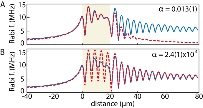
Figure 5 shows two example traces calculated using this procedure (red dashed lines) and compares these to a measured trace (blue line) of Fig. 2c of the main text. In both A and B, the calculated traces use a single value of the damping for the entire spatial range. These plots highlight that the measured data in the microstrip region are only described well for a large value of the damping, while the data next to the microstrip are only described well for a low value of the damping.
3.2.2 Extracting the damping under the gold structure
To extract the spatial decay length of the spin waves underneath the gold structure from spatial measurements of the ESR contrast (Fig. 2e-f of the main text and Supplementary Fig. 6) we describe using
| (73) |
where is the known maximum ESR contrast and is a normalized NV Rabi frequency resulting from the sum of the spin-wave and direct microstrip fields:
| (74) |
Here, and are the known locations of the edges of the microstrip and gold structure, respectively (see Fig. 2e of the main text), and , , and are extracted from the fits. The spatial decay length is given by the linewidth of the susceptibility in -space and can therefore be related to the damping parameter by Taylor expanding in Eq. (29) to get:
| (75) |
Solving , we find
| (76) |
which yields the relation between the spatial decay length and
| (77) |
where we calculate and (defined in Eqs. (25) and (26)) and the spin-wave group velocity from the spin-wave dispersion.
This fit procedure is used to extract the damping from the data in Fig. 2f of the main text, as well as to determine the frequency dependence of the damping underneath the gold structure, for which the data traces and fits are shown in Fig. 6. The extracted values of the damping are plotted in Fig. 2d of the main text.
3.2.3 Three-magnon scattering threshold
The three-magnon scattering process is enabled for spin waves of frequency at least twice that of the bottom of the spin-wave band (), which shifts with the applied magnetic field. In the main text, we see this threshold at 2.39 GHz (Fig. 3). From the spin-wave dispersion (Eq. (29)), we find that this frequency corresponds to the frequency at which the NV ESR transition and cross (Fig. 7).
References
- [1] D. D. Stancil & A. Prabhakar, Spin Waves, (Springer, 2009).
- [2] A. V. Chumak, V. I. Vasyuchka, A. A. Serga, & B. Hillebrands, Magnon spintronics, Nature Physics 11, 453–461 (2015).
- [3] A. Barman, G. Gubbiotti, S. Ladak, A. O. Adeyeye, M. Krawczyk, J. Gräfe, C. Adelmann, S. Cotofana, A. Naeemi, V. I. Vasyuchka, et al., The 2021 Magnonics Roadmap, Journal of Physics: Condensed Matter (in press) (2021).
- [4] T. Fischer, M. Kewenig, D. A. Bozhko, A. A. Serga, I. I. Syvorotka, F. Ciubotaru, C. Adelmann, B. Hillebrands, & A. V. Chumak, Experimental prototype of a spin-wave majority gate, Applied Physics Letters 110, 152401 (2017).
- [5] G. Talmelli, T. Devolder, N. Träger, J. Förster, S. Wintz, M. Weigand, H. Stoll, M. Heyns, G. Schütz, I. P. Radu, J. Gräfe, F. Ciubotaru, & C. Adelmann, Reconfigurable submicrometer spin-wave majority gate with electrical transducers, Science Advances 6, eabb4042 (2020).
- [6] Q. Wang, M. Kewenig, M. Schneider, R. Verba, F. Kohl, B. Heinz, M. Geilen, M. Mohseni, B. Lägel, F. Ciubotaru, C. Adelmann, C. Dubs, S. D. Cotofana, O. V. Dobrovolskiy, T. Brächer, P. Pirro, & A. V. Chumak, A magnonic directional coupler for integrated magnonic half-adders, Nature Electronics 3, 765–774 (2020).
- [7] A. V. Chumak, A. A. Serga, & B. Hillebrands, Magnon transistor for all-magnon data processing, Nature Communications 5, 4700 (2014).
- [8] L. J. Cornelissen, J. Liu, B. J. van Wees, & R. A. Duine, Spin-Current-Controlled Modulation of the Magnon Spin Conductance in a Three-Terminal Magnon Transistor, Physical Review Letters 120, 097702 (2018).
- [9] J. Sinova, S. O. Valenzuela, J. Wunderlich, C. H. Back, & T. Jungwirth, Spin Hall effects, Reviews of Modern Physics 87, 1213–1260 (2015).
- [10] L. J. Cornelissen, J. Liu, R. A. Duine, J. B. Youssef, & B. J. Van Wees, Long-distance transport of magnon spin information in a magnetic insulator at room temperature, Nature Physics 11, 1022–1026 (2015).
- [11] I. Bertelli, J. J. Carmiggelt, T. Yu, B. G. Simon, C. C. Pothoven, G. E. Bauer, Y. M. Blanter, J. Aarts, & T. van der Sar, Magnetic resonance imaging of spin-wave transport and interference in a magnetic insulator, Science advances 6, eabd3556 (2020).
- [12] A. Gruber, A. Dräbenstedt, C. Tietz, L. Fleury, J. Wrachtrup, & C. Von Borczyskowski, Scanning confocal optical microscopy and magnetic resonance on single defect centers, Science 276, 2012–2014 (1997).
- [13] L. Rondin, J. P. Tetienne, T. Hingant, J. F. Roch, P. Maletinsky, & V. Jacques, Magnetometry with nitrogen-vacancy defects in diamond, Reports on Progress in Physics 77, 056503 (2014).
- [14] T. Rosskopf, A. Dussaux, K. Ohashi, M. Loretz, R. Schirhagl, H. Watanabe, S. Shikata, K. M. Itoh, & C. L. Degen, Investigation of surface magnetic noise by shallow spins in diamond, Physical Review Letters 112, 147602 (2014).
- [15] F. Casola, T. van der Sar, & A. Yacoby, Probing condensed matter physics with magnetometry based on nitrogen-vacancy centres in diamond, Nature Reviews Materials 3, 17088 (2018).
- [16] M. Mohseni, R. Verba, T. Brächer, Q. Wang, D. A. Bozhko, B. Hillebrands, & P. Pirro, Backscattering Immunity of Dipole-Exchange Magnetostatic Surface Spin Waves, Physical Review Letters 122, 197201 (2019).
- [17] T. Yu, Y. M. Blanter, & G. E. W. Bauer, Chiral Pumping of Spin Waves, Physical Review Letters 123, 247202 (2019).
- [18] P. Andrich, C. F. de las Casas, X. Liu, H. L. Bretscher, J. R. Berman, F. J. Heremans, P. F. Nealey, & D. D. Awschalom, Long-range spin wave mediated control of defect qubits in nanodiamonds, npj Quantum Information 3, 28 (2017).
- [19] P. Pincus, Excitation of spin waves in ferromagnets: eddy current and boundary condition effects, Physical Review 118, 658–664 (1960).
- [20] M. Kostylev, Strong asymmetry of microwave absorption by bilayer conducting ferromagnetic films in the microstrip-line based broadband ferromagnetic resonance, Journal of Applied Physics 106, 043903 (2009).
- [21] M. A. Schoen, J. M. Shaw, H. T. Nembach, M. Weiler, & T. J. Silva, Radiative damping in waveguide-based ferromagnetic resonance measured via analysis of perpendicular standing spin waves in sputtered permalloy films, Physical Review B 92, 184417 (2015).
- [22] Y. Li & W. E. Bailey, Wave-Number-Dependent Gilbert Damping in Metallic Ferromagnets, Physical Review Letters 116, 117602 (2016).
- [23] M. Kostylev, Coupling of microwave magnetic dynamics in thin ferromagnetic films to stripline transducers in the geometry of the broadband stripline ferromagnetic resonance, Journal of Applied Physics 119, 013901 (2016).
- [24] J. W. Rao, S. Kaur, X. L. Fan, D. S. Xue, B. M. Yao, Y. S. Gui, & C. M. Hu, Characterization of the non-resonant radiation damping in coupled cavity photon magnon system, Applied Physics Letters 110, 262404 (2017).
- [25] S. A. Bunyaev, R. O. Serha, H. Y. Musiienko-Shmarova, A. J. Kreil, P. Frey, D. A. Bozhko, V. I. Vasyuchka, R. V. Verba, M. Kostylev, B. Hillebrands, G. N. Kakazei, & A. A. Serga, Spin-wave relaxation by Eddy Currents in Y3Fe5O12/Pt bilayers and a way to suppress it, Physical Review Applied 14, 024094 (2020).
- [26] J. D. Cutnell & K. W. Johnson, Physics, (Wiley, Hoboken, 1997).
- [27] C. Mathieu, V. T. Synogatch, & C. E. Patton, Brillouin light scattering analysis of three-magnon splitting processes in yttrium iron garnet films, Physical Review B 67, 104402 (2003).
- [28] H. Schultheiss, X. Janssens, M. Van Kampen, F. Ciubotaru, S. J. Hermsdoerfer, B. Obry, A. Laraoui, A. A. Serga, L. Lagae, A. N. Slavin, B. Leven, & B. Hillebrands, Direct current control of three magnon scattering processes in spin-valve nanocontacts, Physical Review Letters 103, 157202 (2009).
- [29] T. Schneider, A. A. Serga, A. V. Chumak, C. W. Sandweg, S. Trudel, S. Wolff, M. P. Kostylev, V. S. Tiberkevich, A. N. Slavin, & B. Hillebrands, Nondiffractive subwavelength wave beams in a medium with externally controlled anisotropy, Physical Review Letters 104, 197203 (2010).
- [30] T. Wimmer, M. Althammer, L. Liensberger, N. Vlietstra, S. Geprägs, M. Weiler, R. Gross, & H. Huebl, Spin Transport in a Magnetic Insulator with Zero Effective Damping, Physical Review Letters 123, 257201 (2019).
- [31] M. Schneider, T. Brächer, D. Breitbach, V. Lauer, P. Pirro, D. A. Bozhko, H. Y. Musiienko-Shmarova, B. Heinz, Q. Wang, T. Meyer, F. Heussner, S. Keller, E. T. Papaioannou, B. Lägel, T. Löber, C. Dubs, A. N. Slavin, V. S. Tiberkevich, A. A. Serga, B. Hillebrands, & A. V. Chumak, Bose–Einstein condensation of quasiparticles by rapid cooling, Nature Nanotechnology 15, 457–461 (2020).
- [32] T. L. Gilbert, A phenomenological theory of damping in ferromagnetic materials, IEEE Transactions on Magnetics 40, 3443–3449 (2004).
- [33] K. Y. Guslienko & A. N. Slavin, Magnetostatic Greens functions for the description of spin waves in finite rectangular magnetic dots and stripes, Journal of Magnetism and Magnetic Materials 323, 2418–2424 (2011).
- [34] A. Brataas, Y. Tserkovnyak, & G. E. Bauer, Magnetization dissipation in ferromagnets from scattering theory, Physical Review B 84, 054416 (2011).