A Novel SEPIC-Ćuk Based High Gain Solar Micro-Inverter for Grid Integration
Abstract
Solar micro-inverters are becoming increasingly popular as they are modular, and they posses the capability of extracting maximum available power from the individual photovoltaic (PV) modules of a solar array. For realizing micro-inverters single stage transformer-less topologies are preferred as they offer better power evacuation efficacy. A SEPIC-Ćuk based transformer-less micro-inverter, having only one high frequency switch and four line frequency switches, is proposed in this paper. The proposed converter can be employed to interface a 35 V PV module to a 220 V single phase ac grid. As a very high gain is required to be achieved for the converter, it is made to operate in discontinuous conduction mode (DCM) for all possible operating conditions. Since the ground of the each PV modules is connected to the ground of the utility, there is no possibility of leakage current flow between the module and the utility. Detailed simulation studies are carried out to ascertain the efficacy of the proposed micro-inverter. A laboratory prototype of the inverter is fabricated, and detailed experimental studies are carried out to confirm the viability of the proposed scheme.
Index Terms:
Solar PV, Micro-inverter, Ćuk converter, SEPIC, DCM, dc-ac Conversion.I Introduction
Though the fossil fuel based power generation remains to be the dominant source of electrical energy, harvesting of energy from the renewable sources (solar, wind etc.) are strongly being encouraged as they are more environment friendly, and inexhaustible in nature. In India, as the solar energy is abundant all over the country throughout the year, it is becoming a viable alternative to the conventional methods of generation of electrical energy. The Ministry of New & Renewable Energy, Govt. of India, has set a target of 100 GW grid connected solar power generation by the year 2021-22 under National Solar Mission, out of which 40 GW should be from the rooftop installations [1]. The solar modules are generally interfaced to the utility by employing the following configurations, (i) central inverter, (ii) string inverter and (iii) micro-inverter. The major advantages of the micro-inverter over the central and string inverter are as follows [2],
-
•
capability of individual maximum power point tracking (MPPT) of the PV modules during non-uniform shading,
-
•
the aspect of modularity bestows it with the flexibility in future expansion of the plant whenever required,
-
•
the existence of plug and play feature imparts flexibility in operation and coordination of the system.
Typically, the power rating of a micro-inverter is 250-350 W, and hence their efficiency remains to be low compared to that of the schemes based on central and string inverters. In order to improve the efficiency of micro-inverters, lower number of power conversion stages are incorporated [3]. In order to accomplish this feature, transformer-less single stage topologies for micro-inverter are generally preferred [4]. However, in case of transformer-less topologies, there exists a path for the leakage current to flow through the parasitic capacitance of the PV module to the grid [5, 6]. The flow of leakage current deteriorates the life of the modules. Further, it posses hazard to the working personnel as the potential of the mountings of the PV module may become high with respect to the mother earth. Hence, the magnitude of the leakage current needs to be limited within the standard limit as stipulated by various regulatory authorities [7].
Generally the MPP voltage of a PV module is 35 V. However it has to be interfaced to the single phase 110/230 V grid. Hence, the micro-inverter needs to have a very high gain, which is one of the main challenges to be addressed.
The requirements pertaining to topological configuration, and its design can be summarized as follows,
-
•
the magnitude of the leakage current must be within the limits as specified by various standards,
-
•
the inverter system should have a very high voltage gain to interface a PV module having a of 35 V to a single phase 110/230 V ac grid,
-
•
the micro-inverter needs to made as compact as possible.
There are several single stage non-isolated topologies reported in the literature [4]. The issue related to the leakage current has been addressed to by shorting the module ground with that of the ac grid [8, 9, 10, 11, 12, 13, 14, 15]. A buck-boost based micro-inverter topology with only one high frequency switch is proposed in [8]. In [9], a buck-boost based and in [10], a Ćuk converter based single stage micro-inverter topologies are reported, wherein the PV module and the ac grid shares the common ground. In [9], the MPP voltage is chosen to be 55 V, and the ac grid voltage is considered to be 110 V. Though the converter is operated in continuous conduction mode (CCM), the source current is discontinuous thereby increasing the filtering requirement at the input side. Moreover, the switches are operated in such a way that, the decoupling of second order harmonic component is achieved at the terminals of the PV module. In [10], Ćuk derived topology is reported wherein, 5 high frequency (HF) switches are employed, and the converter is operated in CCM. A similar power decoupling strategy, as reported in [9], is incorporated in the topology presented in[10], and reported in [12]. The designed switching frequency in all the aforesaid configurations are 50 kHz. In [11] and [13], a four switch topology with different switching configurations have been proposed. However, all the switches of these converters [9, 10, 11, 13] operate at high frequency. All these converters are designed to be operated in CCM. This facilitates the inverters to get interfaced to a single phase voltage level up to 110 V. A modification to the circuit reported in [10] has been accomplished by adding another HF switch for controlling the reactive power fed to the grid, and is presented in [14]. However, the designed switching frequency is 10 kHz, and hence the size of passive elements are significantly large. A three switch micro-inverter topology with common ground is reported in [15] wherein the voltage gain of the converter can be made both positive and negative, and therefore it does not require the service of an unfolding circuit but then it involves three inductors in the main converter.
In India, the ac distribution voltage level is 220 V. However, all the aforementioned converters are designed to get interfaced to single phase 110 V system, and hence they are not suitable for Indian conditions. However in [16] a micro-inverter topology is presented, which can be interfaced to a single phase 220 V grid. However, it requires six switches, out of which, two are required to be high frequency switches. In view of this an effort has been made in this paper to design a transformer-less micro-inverter suitable for getting interfaced to a single phase 220 V grid while utilizing only one high frequency switch and four line frequency switches in order to reduce the switch count and reliability of the system.
In order to accomplish these features a SEPIC-Ćuk based micro-inverter topology is proposed in [17] by the authors of the current paper. The converter is operated in SEPIC mode during positive half cycle and in Ćuk mode during negative half cycle. By merging SEPIC and Ćuk configurations into one topology, the number of HF switches has been reduced to one. The designed switching frequency of the system is 100 kHz, hence the size of passive elements have been reduced considerably. The presence of the common ground between the module and the grid ensures negligible leakage current flow. However, the circuit was explored for getting interfaced to single phase 110 V ac grid. In this paper, an attempt has been made to get interfaced to a single phase 220 V ac, which is suitable for Indian distribution network, utilizing the converter proposed in [17] from a PV module having of 35 V. Detailed simulation studies are carried out on MATLAB/Simulink platform to ascertain the effectiveness of the proposed converter. A semi-engineered laboratory prototype of the inverter has been fabricated, and detailed experimental studies are carried out to confirm the viability of the proposed scheme.
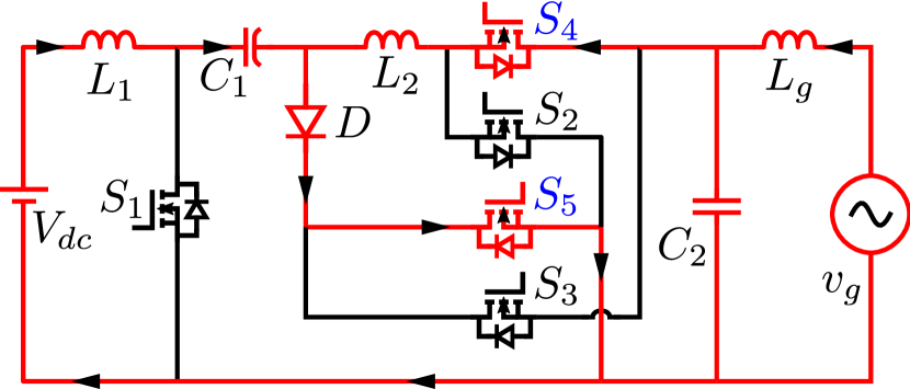
II Principle of Operation of the Proposed Topology
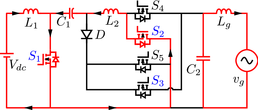
The schematic diagram of the proposed SEPIC-Ćuk based micro-inverter is shown in Fig. 1. Four line frequency switches are utilized to derive the combine effect of SEPIC and Ćuk configuration. In [17] the IGBTs are used to realize the line frequency switches. In this paper MOSFETs are used instead of IGBTs to reduce the losses. The diode, is employed to block the reverse current flow through the four MOSFETs. As sinusoidal current is required to be injected to the grid, the high frequency switch is applied with switching pulses which are obtained by comparing the rectified sine wave with a triangular carrier wave. The instantaneous duty ratio of is determined by multiplying a rectified sine wave with the peak duty ratio, . The switch is operated with when the instantaneous grid voltage is at its peak. The current through is a rectified sine wave having high frequency switching harmonics superimposed on it. In order to transform this rectified current into a sinusoidal waveform the four switches, , and are appropriately switched. The output capacitor, filters out the high frequency harmonic components form the output current.

The inductors of the converter can be chosen in such a way so that the converter can be operated either in CCM or in DCM. In CCM the voltage gain of both SEPIC and Ćuk converter is , wherein is the duty ratio of the converter. However, for interfacing the 35 V module to a 220 V ac grid whose peak voltage is 311 V, the requirement of the duty ratio at the peak of the ac grid voltage is required to be maintained at 0.9. Operating the inverter at this high duty ratio, would reduce the operating efficiency significantly. In order to overcome this limitation, the proposed topology is operated in DCM to obtain high voltage gain while maintaining reduced duty ratio compared to that of CCM operation. In case of a SEPIC and Ćuk converter, current through both and does not become zero either in CCM or DCM mode of operation[18, 19]. Further, the DCM operation ensures that turn on switching loss of is negligible. But this is achieved at the cost of increased peak current that flows through the input inductor.
III Modes of Operation and Analysis
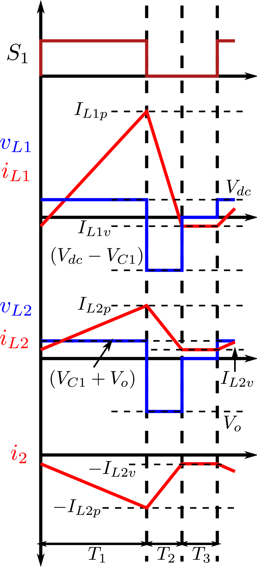
In order to simplify the analysis of the inverter, a dc source, is used instead of a PV module. The convention of voltage polarity and current direction is shown in Fig. 1. Since the switching frequency is very high compared to that of the line frequency, it is assumed that, the output voltage and current requirement is almost constant throughout the switching time period (). The ripple in the voltages in the capacitors, and can be considered to be negligible. The average value of and over a switching time period are assumed to be and respectively. The current and voltage waveforms over a switching cycle is shown in Fig. 4. The switching time period () is divided into three time intervals as follows, (i) , (ii) and (iii) respectively. As , therefore .
III-A Positive half cycle (SEPIC mode)
Switch and both are turned on, while and are kept off. At steady state, as the switching time average voltages across and are zero,
| (1) |
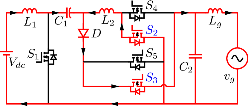
III-A1 Mode I ()
is turned on and the current through increases as it flows through the path, as shown in Fig. 3(a). The intermediate capacitor, gets discharged while the current flowing through increases as it flows through the path, . The capacitor, supplies power to the grid in this interval. The diode, blocks the current through the switch even though it is receiving the gating pulse. Hence,
| (2) | ||||
| (3) | ||||
| (4) |
where, and .
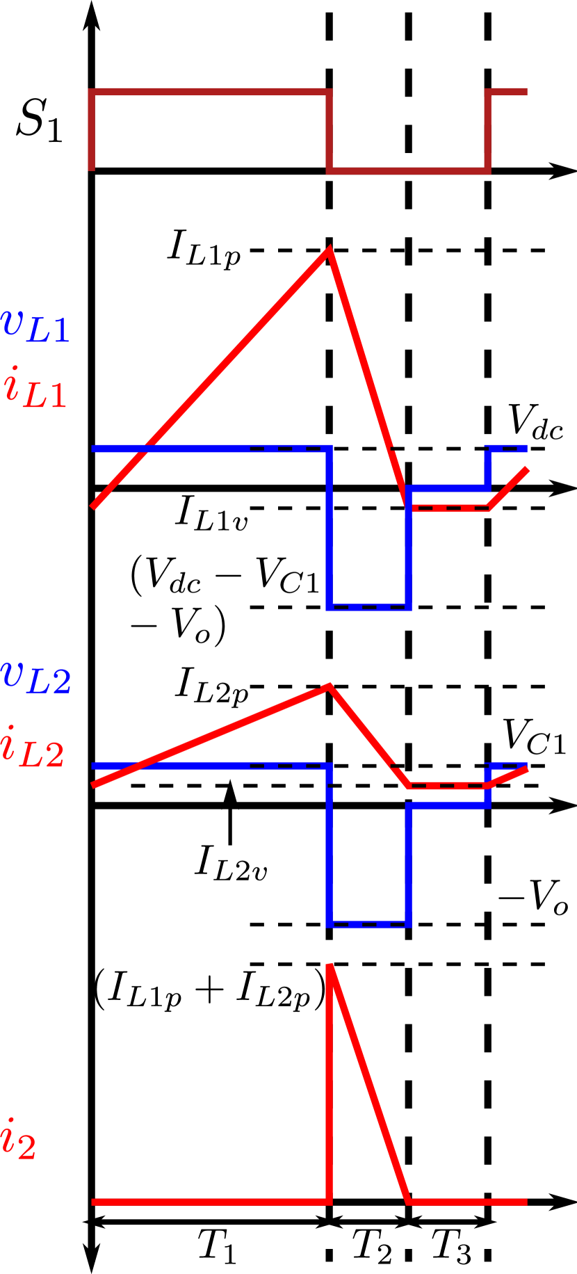
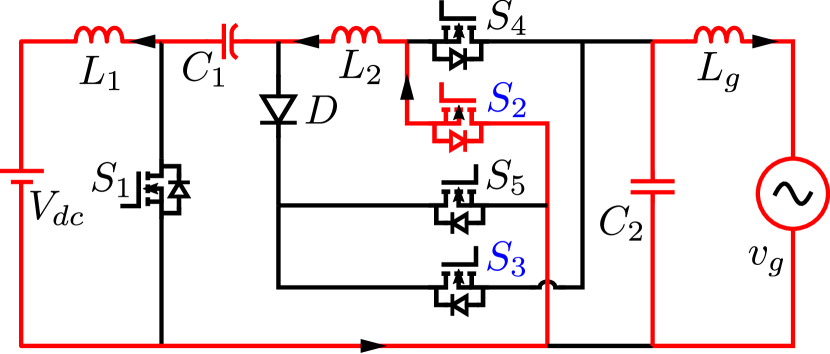
III-A2 Mode II ()
is turned off. The current flows through the path, as shown in Fig. 3(b) thereby charging . The energy stored in is transferred to the grid as well as to through the path, . This mode ends when . At the end of this mode, let the magnitude of the currents through and be and respectively. Therefore,
| (5) | ||||
| (6) | ||||
| (7) |
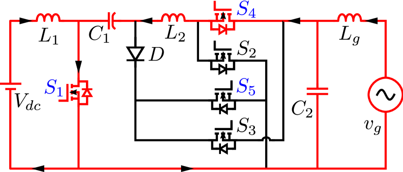
III-A3 Mode III ()
This mode starts when the current through the diode, becomes zero. The diode turns off and blocks the current flowing through . The current path in this mode is as shown in Fig. 3(c). Since , the currents in the inductors will remain unchanged in this mode. The capacitor supplies power to the grid in this interval. Hence,
| (8) |
| (9) |
III-B Negative half cycle (Ćuk Mode):
Switch and both are turned on, while and are kept off. At steady state, as the switching time average voltages across and are zero,
| (10) |
III-B1 Mode I ()
is turned on and the current through increases as it flows through the path, as shown in Fig. 3(a). The intermediate capacitor, gets discharged while the current flowing through increases as it flows through the path, . The diode, blocks the current through the switch even though it is receiving the gating pulse. Hence,
| (11) | ||||
| (12) |
III-B2 Mode II ()
is turned OFF. The current flows through the path, as shown in Fig. 3(b) thereby charging . The energy stored in is transferred to the load as well as to through the path, . This mode ends when . At the end of this mode, let the magnitude of the currents through and be and respectively. Therefore,
| (13) | |||
| (14) |
III-B3 Mode III ()
This mode starts when the current through the diode, becomes zero. The diode turns off and blocks the current flowing through . The current path in this mode is as shown in Fig. 3(c). Since , the currents in the inductors will remain unchanged in this mode. Hence,
| (15) |
Solving (11)–(15), the expression for the voltage gain can be obtained as,
| (16) |
III-C Combined operation
From (9) and (16) the common expression for the voltage gain can be written as,
| (17) |
From (1) and (10), it can be inferred that, the expression for is different in the positive and in the negative half cycle. By substituting the expression of from (1) and (10) to (2), (3), (5), (6), (11), (12), (13) and (14), the model of the system can be simplified as follows:
| (18) | ||||
| (19) |
From Fig. 4, in both the half cycles the expression of switching time average of the dc side current is obtained as,
| (20) |
Further, from Fig. 4 it can be observed that in the positive half cycle the wave shape of in a switching time period is different from that in the negative half cycle. Let the switching time average of is , and it can be approximated to be equal to the grid current, . It can be noted that, this waveform is exactly negative to that of in Ćuk mode of operation. Hence, in this mode, is equal to the switching time average of but with a negative sign. Therefore,
| (21) |
For SEPIC mode, can be expressed as,
| (22) |
Considering the system to be loss-less,
| (23) |
If, has to be positive,
| (26) |
needs to be satisfied. However in that case when becomes zero at the zero crossing instants as per (26), needs to assume a negative value which is not possible. Hence the value of is chosen so that, remains negative for all possible operating conditions.
In SEPIC mode of operation, the average current through is given by,
| (27) |
From (22) and (27) it can be inferred that, is equal to in SEPIC mode of operation as well. Hence in combined operation, , which means that, can be manipulated to control . Since the absolute value of the output current expression is same in both the half cycles it can be inferred that (25) and (26) are also valid for Ćuk mode of operation as well. Therefore the design condition for remains the same in both the half cycles.
Substituting in (20),
| (28) |
Since the output voltage and current is sinusoidal and they are in phase with each other,
| (29) |
wherein, is the average current drawn from PV module. Further, and being positive, its expression can be written as
| (31) |
Hence needs to be a rectified sine wave with an amplitude of . The value of will be dictated by the irradiance level experienced by the solar PV module.
IV Control Configuration
In the Fig. 5 the schematic of the control block diagram is shown. The rms value of the output current is measured and compared with the reference, , which is to be generated by the MPPT controller. The PI controller processes the error so obtained to determine . A rectified sinusoidal signal having an amplitude of unity is multiplied with to obtain the instantaneous duty ratio, . The reference sine wave is generated by employing a single phase PLL. Switching pulses for are obtained by comparing with a triangular carrier wave.

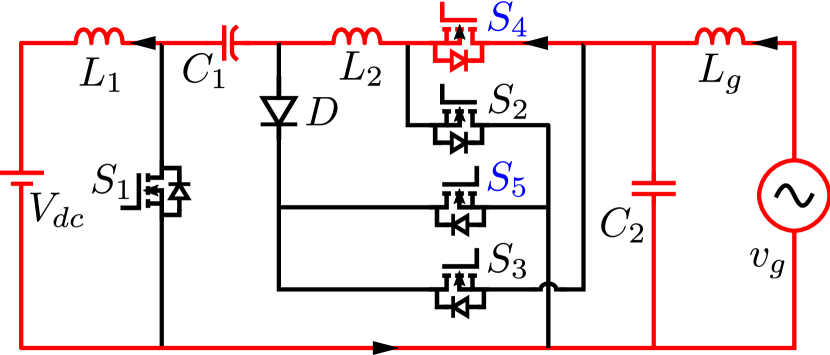
Switches and are turned on during the positive half cycle of the reference sine wave to operate the circuit in SEPIC mode, while and are turned on during its negative half cycle to operate the circuit in Ćuk mode.
V Selection of Parameters
V-A Design of input inductor ()
At the limiting condition, when the converter operates at the verge of discontinuous and continuous mode of operation at the peak of the grid voltage and operating at the rated condition,
| (32) |
where, is the amplitude of the grid voltage, . At this instant, the switching time average of is . Hence,
| (33) |
V-B Design of intermediate capacitor ()
As the average voltage of is less in SEPIC mode of operation, the voltage ripple of is much higher in this mode compared to the operation of the inverter in the Ćuk mode. Hence the design of is carried out considering the operation of the converter in SEPIC mode which is as follows,
| (34) |
V-C Design of output inductor ()
The switching time average current through is the current fed to the grid during this interval. The current ripple in is derived and subsequently the design criterion of is obtained as follows,
| (35) |
V-D Design of output capacitor ()
The output capacitor is chosen so that the cut off frequency, of the filter is way above the grid frequency, , and way below the switching frequency, , i.e. and the value of is obtained to be,
| (36) |
VI Simulated Performance of the Proposed Converter
| Parameters | Values | |
|---|---|---|
| 35 V | ||
| 220 V | ||
| 50 Hz | ||
| 100 kHz | ||
| 194 |
| Parameters | Values | |
|---|---|---|
| , | 8 H, 20 m | |
| , | 100 H, 0.6 | |
| , | 0.47 F, 30 m | |
| , | 0.47 F, 30 m | |
| 1 mH |
Detailed simulation studies of the proposed converter have been carried out on MATLAB/Simulink platform. For simplicity, the grid is replaced by a load resistance while maintaining the voltage across this resistance to be equal to 220 V ac. In a realistic grid connected system, reference output current, would be determined by the MPPT controller. However, in this simplistic system is obtained by employing a PI controller which maintains the terminal voltage of the inverter at 220 V. The parameters chosen for the simulation model along with the parasitic series resistances of the converter are shown in Table I.
The proportional gain and integral gain values of the PI controller used for controlling are chosen to be 0.5 and 60 s-1 respectively.
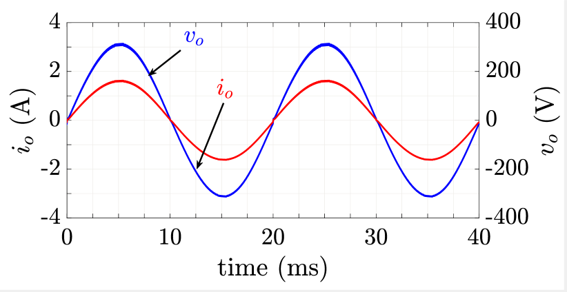
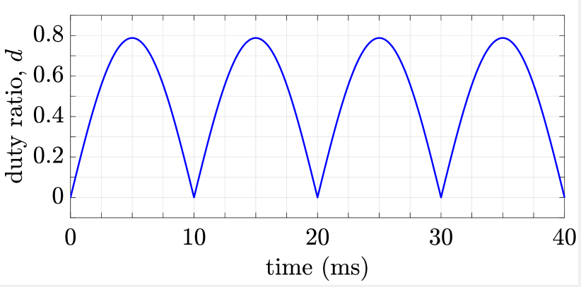
The inverter is operated with the system parameters as depicted in Table I(a). The steady state response of the output voltage and current of the proposed inverter is shown in Fig. 6. It may be noted that the amplitude of the sinusoidal output voltage of the inverter is 311 V. From Fig. 7 it can be inferred that the converter is operated with the peak duty ratio () of 0.8. The THD of the output voltage is found to be 1.21%.
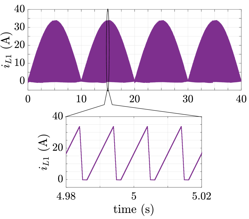
The steady state response of the input inductor current is shown in Fig. 8. It can be inferred from the aforementioned figures that the converter is operating in DCM.

At steady state, the voltage across the intermediate capacitor, is shown in Fig. 9. Form this figure it can be noted that the waveform of in the positive half cycle is different from that in the negative half cycle. This difference arises as the converter operates in SEPIC mode during positive half cycle, and in Ćuk mode during negative half cycle.

The steady state response of output inductor current, is shown in Fig. 10. It can be inferred that the waveform is a rectified sine wave having switching frequency harmonic components.
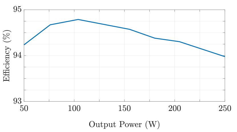
The plot of the estimated efficiency of the inverter with respect to the power level is shown in Fig. 11. For efficiency estimation, the MOSFET, IPW60R024P7 is considered for and MOSFET, IPW60R037P7 is considered for . Although the inverter is developing 220 V ac from an input voltage of 35 V dc, the efficiency of the proposed inverter is comparable with the inverters which are reported in the literature for developing 110 V ac from 35-50 V dc[10, 12, 14].
VII Experimental Validation
In order to confirm the the viability of the proposed inverter, a 250 W semi-engineered laboratory prototype of the micro-inverter is fabricated, and detailed experimental studies have been carried out. The passive components as mentioned in Table I(b) are used to realize the prototype. In order to increase the reliability, thin film capacitors are used. Switch is realized by the MOSFET, IPW60R024P7 while are realized by MOSFET, IPW60R037P7. The controller of the inverter is realized by utilising DSP, TMS320F28355. A 1.5 kW programmable power supply (EPS power supply PSI 9360-15) is used as the input dc source. The photograph of the prototype is shown in Fig. 12.

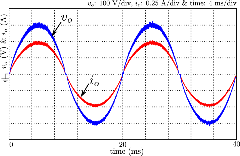
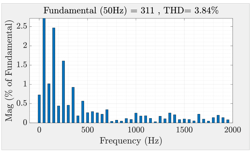
The measured performance of the inverter is shown Fig. 13 wherein the input voltage is maintained at 35 V dc and the load resistance of 660 is connected across its output terminals. It can be noted that the peak of the output voltage developed across the load resistance is 311 V rms. In Fig. 15 the measured waveform of is depicted which indicates that at light load condition the circuit operates in DCM. The operating efficiency of the inverter while it is made to deliver 73 W is found to be 89.5%. The THD in the output voltage is 3.84% (Fig. 14) which is well within the stipulated standards.
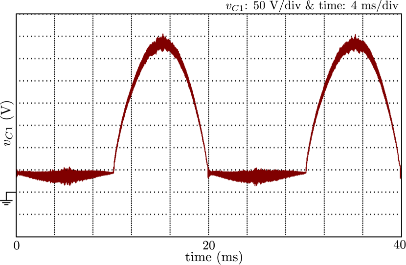
The measured voltage across while the inverter is operating at steady state is shown in Fig. 16 which resembles the simulated waveform of Fig. 9. Since in the positive half cycle, , it can be inferred from Fig. 16 that the input voltage is maintained at 35 V. In negative half cycle the peak value of the waveform is around 350 V since it is the sum of the input voltage and peak of the sinusoidal output voltage, .
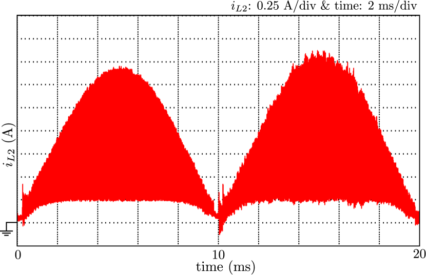
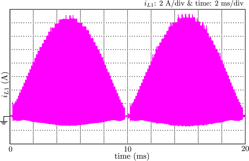
The measured steady state current through is shown in Fig 17. It may be noted that it is polluted with high frequency switching harmonics. It also shows that for this operating condition remains to be positive. However after getting manipulated by the the unfolding and filtering circuits the output current, becomes almost sinusoidal current (Fig. 13) having a THD of 3.84%.
VIII Conclusion
A combined SEPIC-Ćuk based micro-inverter topology has been proposed in this paper. The salient features of the proposed inverter are as follows,
-
•
it operates in SEPIC mode for positive half cycle and in Ćuk mode for negative half cycle
-
•
the inverter is realized by using single high frequency switch thereby improving its reliability and cost
-
•
four line frequency switches are employed to interchange the modes between SEPIC and Ćuk mode, and the switching losses associated with these switches are negligible
-
•
in order to obtain high gain the inverter is made to operated in DCM. The DCM operation also ensures that the turn on loss of the high frequency switch is negligible
-
•
the neutral of the PV module is shorted with that of the grid thereby eliminating the flow of leakage current
The operating principle, detailed mathematical modelling of the system, design guidelines for the passive elements, control strategy are presented in the paper. The viability of the micro-inverter is validated by carrying out detailed simulation and experimental studies.
References
- [1] MNRE, Govt of India. (2020) Overview, MNRE. [Online]. Available: https://mnre.gov.in/img/documents/uploads/0ce0bba7b9f24b32aed4d89265d6b067.pdf
- [2] A. Bidram, A. Davoudi, and R. S. Balog, “Control and Circuit Techniques to Mitigate Partial Shading Effects in Photovoltaic Arrays,” IEEE Journal of Photovoltaics, vol. 2, no. 4, pp. 532–546, 2012.
- [3] D. Meneses, F. Blaabjerg, O. Garcia, and J. A. Cobos, “Review and Comparison of Step-up Transformerless Topologies for Photovoltaic AC-module Application,” IEEE Transactions on Power Electronics, vol. 28, no. 6, pp. 2649–2663, 2013.
- [4] K. Alluhaybi, I. Batarseh, and H. Hu, “Comprehensive Review and Comparison of Single-Phase Grid-Tied Photovoltaic Microinverters,” IEEE Journal of Emerging and Selected Topics in Power Electronics, vol. 8, no. 2, pp. 1310–1329, 2020.
- [5] E. Gubia, P. Sanchis, A. Ursua, J. Lopez, and L. Marroyo, “Ground Currents in Single-Phase Transformerless Photovoltaic Systems,” Progress in photovoltaics: research and applications, vol. 15, no. 7, pp. 629–650, 2007.
- [6] D. Debnath, “Reduced Stage Off-Grid and Buck-Boost Inverter based Grid Connected Solar Photovoltaic Systems,” Ph.D. dissertation, IIT Bombay, 2015.
- [7] W. Li, Y. Gu, H. Luo, W. Cui, X. He, and C. Xia, “Topology Review and Derivation Methodology of Single-Phase Transformerless Photovoltaic Inverters for Leakage Current Suppression,” IEEE Transactions on Industrial Electronics, vol. 62, no. 7, pp. 4537–4551, July 2015.
- [8] H. Patel and V. Agarwal, “A Single-Stage Single-Phase Transformer-Less Doubly Grounded Grid-Connected PV Interface,” IEEE Transactions on Energy Conversion, vol. 24, no. 1, pp. 93–101, March 2009.
- [9] A. Jamatia, V. Gautam, and P. Sensarma, “Single Phase Buck-Boost Derived PV Micro-inverter with Power Decoupling Capability,” in Power Electronics, Drives and Energy Systems (PEDES), 2016 IEEE International Conference on. IEEE, 2016, pp. 1–6.
- [10] V. Gautam and P. Sensarma, “Design of Ćuk-Derived Transformerless Common-Grounded PV Microinverter in CCM,” IEEE Transactions on Industrial Electronics, vol. 64, no. 8, pp. 6245–6254, 2017.
- [11] A. Kumar and P. Sensarma, “A four-switch single-stage single-phase buck–boost inverter,” IEEE Transactions on Power Electronics, vol. 32, no. 7, pp. 5282–5292, 2017.
- [12] A. Jamatia, V. Gautam, and P. Sensarma, “Power Decoupling for Single-Phase PV System Using uk Derived Microinverter,” IEEE Transactions on Industry Applications, vol. 54, no. 4, pp. 3586–3595, July 2018.
- [13] A. Kumar and P. Sensarma, “New switching strategy for single-mode operation of a single-stage buck–boost inverter,” IEEE Transactions on Power Electronics, vol. 33, no. 7, pp. 5927–5936, 2018.
- [14] M. Rajeev and V. Agarwal, “Analysis and Control of a Novel Transformer-Less Microinverter for PV-Grid Interface,” IEEE Journal of Photovoltaics, 2018.
- [15] A. Sarikhani, M. M. Takantape, and M. Hamzeh, “A Transformerless Common-Ground Three-Switch Single-Phase Inverter for Photovoltaic Systems,” IEEE Transactions on Power Electronics, vol. 35, no. 9, pp. 8902–8909, 2020.
- [16] A. Bhattacharya, A. R. Paul, and K. Chatterjee, “A Single Phase Single Stage SEPIC-ĆUK Based Non-Isolated High Gain and Efficient Micro-Inverter,” in 2019 IEEE 46th Photovoltaic Specialists Conference (PVSC), 2019, pp. 0708–0715.
- [17] A. R. Paul, A. Bhattacharya, and K. Chatterjee, “A Novel SEPIC-Ćuk Based High Gain Solar Micro-Inverter for Integration to Grid,” in 2019 National Power Electronics Conference (NPEC), 2019, pp. 1–5.
- [18] Z. Shi, K. Cheng, and S. Ho, “Boundary Condition Analysis for Ćuk, SEPIC and Zeta Converters Using Energy Factor Concept,” Journal of Circuits, Systems and Computers, vol. 22, 02 2013.
- [19] V. Eng and C. Bunlaksananusorn, “Modeling of a SEPIC Converter Operating in Discontinuous Conduction Mode,” in 2009 6th International Conference on Electrical Engineering/Electronics, Computer, Telecommunications and Information Technology, vol. 01, 2009, pp. 140–143.