Molecular beam deposition of a new layered pnictide
with distorted Sb square nets
Abstract
While the family of layered pnictides ( : rare or alkaline earth metals, : transition metals, : Sb/Bi) can host Dirac dispersions based on Sb/Bi square nets, nearly half of them has not been synthesized yet for possible combinations of the and cations. Here we report the fabrication of EuCdSb2 with the largest -site ionic radius, which is stabilized for the first time in thin film form by molecular beam deposition. EuCdSb2 crystallizes in an orthorhombic structure and exhibits antiferromagnetic ordering of the Eu magnetic moments at K. Our successful growth will be an important step for further exploring novel Dirac materials using film techniques.
Dirac materials with linear energy dispersions have attracted growing attention in the light of exploring new compounds and elucidating their magnetotransport Wehling et al. (2014). In particular, Dirac dispersions interacting with magnetism have significant potential for producing rich quantum transport Jungwirth et al. (2018); Šmejkal et al. (2018); Shao et al. (2019). Recently, ternary layered pnictides ( : rare or alkaline earths, : transition metals, : Sb/Bi) have been reported to host highly anisotropic Dirac or Weyl dispersions Masuda et al. (2016, 2018); Liu et al. (2019); Sakai et al. (2020); Ling et al. (2018); Kealhofer et al. (2018); Weber et al. (2018); Ramankutty et al. (2018); Qiu et al. (2019); Soh et al. (2019); Park et al. (2011); Wang et al. (2012); Lee et al. (2013); Yan et al. (2017); Liu et al. (2017); Klemenz et al. (2019, 2020); Takahashi et al. (2020), and unprecedented quantum transport has been observed originating from the interplay between the Dirac dispersion and magnetic ordering, as exemplified by bulk half-integer quantum Hall effect in EuMnBi2 Masuda et al. (2016, 2018), BaMnSb2 Liu et al. (2019); Sakai et al. (2020), and SrMnSb2 Ling et al. (2018). Therefore, exploring new compounds especially with magnetic and/or ions is important for systematically investigating their unique magnetotransport.
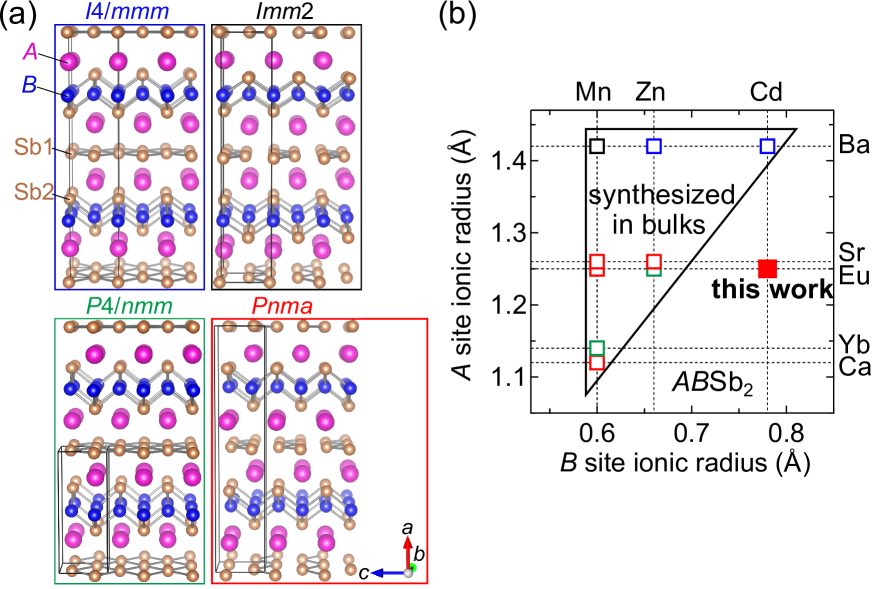
As summarized in Fig. 1(a), there are four space groups (4/, 2, 4/, and ) for Sb2. Sb2 have two types of Sb atoms in the unit cell: one with valence (defined as Sb1) consisting of the Sb net which hosts Dirac or Weyl dispersions and the other with valence (defined as Sb2) forming Sb tetrahedra around the -site cations, which are separated by layers. The -site cations are coincidently stacked across the Sb1 net in and , while they are staggeredly stacked in and . The Sb1 square nets are slightly distorted in and , resulting in a zig-zag chainlike structure along the -axis.
As seen in the map in Fig. 1(b), it becomes difficult to stabilize Sb2 with smaller -site and larger -site ionic radii, and nearly half of Sb2 has not been synthesized yet for all the possible combinations of the and cations Weber et al. (2018); Ramankutty et al. (2018); Kealhofer et al. (2018); Qiu et al. (2019); Soh et al. (2019); G. and H. (1977); Brechtel et al. (1981); Yi et al. (2017); Gong et al. (2020); You et al. (2019); May et al. (2009); Park et al. (2016); Liu et al. (2016); Huang et al. (2017, 2020); He et al. (2017); Ling et al. (2018); Wang et al. (2018); Liu et al. (2019c); Wang et al. (2020); Liu et al. (2019b). In this lower right region of the map in Fig. 1(b), phase separation may occur, for example, from EuCdSb2 to EuSb2 with valence Hulliger and Schmelczer (1978); Ohno2020 and EuCd2Sb2 with valence Su et al. (2020), because Sb2 has different and valence states in one structure. Especially in the case of Cd, its high vapor pressure also makes the fabrication difficult.
In this context, developing techniques for stabilizing new Sb2 compounds is strongly called for advancing this research field. Here we report the fabrication of its new member EuCdSb2, which is stabilized for the first time in thin film form by molecular beam deposition. EuCdSb2 crystallizes in the orthorhombic structure and exhibits unique nonmetallic transport.
Single-crystalline (0001) Al2O3 substrates were annealed at 850 ∘C in a base pressure about Pa and then EuCdSb2 films were grown on it in an Epiquest RC1100 chamber Nakazawa et al. (2019). The molecular beams were simultaneously provided from conventional Knudsen cells containing 3N Eu, 6N Cd, and 6N Sb. The growth temperature was set at 390 ∘C, and the beam equivalent pressures, measured by an ionization gauge, were set to 1.210-5 Pa for Eu, 5.010-4 Pa for Cd, and 8.510-6 Pa for Sb (for details see Supplementary Materials Supplement ). To avoid Cd deficiency, the Cd flux was set 40 times higher than the Eu flux. The film thickness was typically set at 25 nm for structural characterization and magnetotransport measurements, and 50 nm for magnetization measurements. The growth rate was about 0.07 /s. Magnetotransport was measured by a standard four-probe method for 200 m-width multi-terminal Hall bars. Longitudinal and Hall resistivities were measured up to 22.4 T using a non-destructive pulsed magnet Uchida et al. (2017) at the International MegaGauss Science Laboratory in the Institute for Solid State Physics at the University of Tokyo. Temperature dependence of the resistivity and magnetization was measured using a Quantum Design Physical Properties Measurement System and a Magnetic Property Measurement System, respectively.
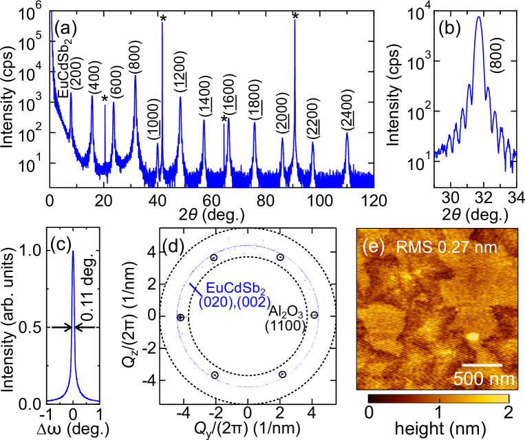
Figure 2 shows structural characterization of an obtained EuCdSb2 film. As shown in the x-ray diffraction (XRD) -2 scan in Fig. 2(a), the reflections from the (200) EuCdSb2 lattice planes are observed without any impurity phases. Its out-of-plane lattice constant along the -axis is calculated to be Å. As confirmed in Fig. 2(b), clear Laue fringes indicate highly coherent lattice ordering along the out-of-plane direction. A rocking curve taken for the (800) film peak in Fig. 2(c) is very sharp with a full width at half maximum of degrees, ensuring high crystallinity of the film. On the other hand, the in-plane XRD reciprocal space map shown in Fig. 2(d) suggests that the - and -axes are rather randomly oriented forming domain structures. In-plane and EuCdSb2 peaks are also indiscernible, indicating that the in-plane lattice constants of the - and -axes are almost the same. The atomic force microscopy image in Fig. 2(e) reveals a flat surface with a root mean square (RMS) roughness of nm.
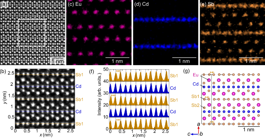
The crystal structure of this new compound is closely examined by taking high-angle annular dark-field scanning transmission electron microscopy (HAADF-STEM) images. A cross-sectional image of the EuCdSb2 film in Fig. 3(a) shows clear stacking of the Sb square nets and other layers. Its in-plane lattice constant along the -axis is calculated to be 4.47 Å by comparing with the -axis length determined by the XRD -2 scan. Higher resolution HAADF-STEM image and corresponding elemental maps in Fig. 3(b)-3(e) reveal additional details of the atomic arrangement. Staggered stacking of Eu atoms across the Sb1 layers rules out the and structures among the four possible space groups as shown in Fig. 1(a). As confirmed in the intensity profiles in Fig. 3(f), moreover, alternate left and right shifts of the Sb atoms are clearly resolved in the Sb1 layers, in contrast to the equally spaced Cd atoms. These Sb shifts correspond to the distorted Sb square nets as shown in Fig. 3(g) and thus we conclude that the EuCdSb2 crystal structure is . The structure is a nonsymmorphic structure which protects band crossings of Dirac dispersions Klemenz et al. (2020).
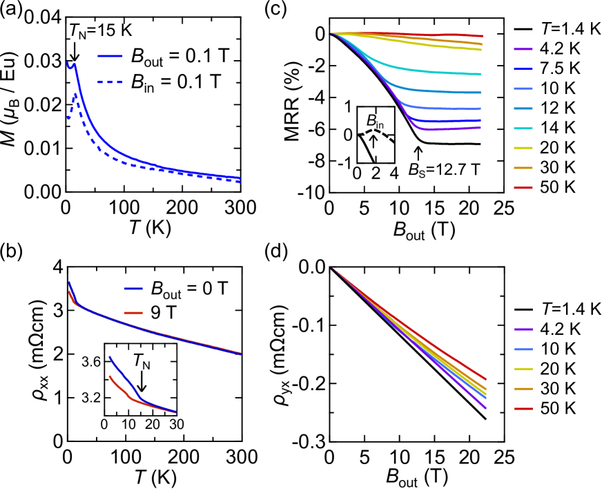
Figure 4 summarizes fundamental transport and magnetic properties of the EuCdSb2 films. Temperature dependence of the magnetization in Fig. 4(a) shows a kink at K, which is ascribed to antiferromagnetic (AFM) ordering of the Eu magnetic moments as detailed in the following. This kink is observed much sharper for the in-plane field, while an almost constant behavior below is found for the out-of-plane field. This indicates that the Eu magnetic moments are antiferromagnetically ordered in the in-plane. Similar to other Eu compounds Masuda et al. (2016, 2018); Yi et al. (2017); Soh et al. (2019); Gong et al. (2020); Wang et al. (2020), the Eu magnetic moments of EuCdSb2 probably forms the A-type AFM structure where ferromagnetic (FM) in-plane layers are antiferromagnetically stacked along the out-of-plane direction. Figure 4(b) shows the nonmetallic temperature dependence of the longitudinal resistivity. A drastic upturn at K coincides with the AFM ordering, as also confirmed by its shift upon increasing the magnetic field. This nonmetallic temperature dependence is a common feature only with EuMnSb2 Yi et al. (2017); Soh et al. (2019); Gong et al. (2020), and the further upturn below appears only in EuCdSb2, while other Sb2 compounds shown in Fig. 1(b) exhibit metallic behavior He et al. (2017); May et al. (2009); Park et al. (2016); Liu et al. (2016); Huang et al. (2017); Ling et al. (2018); Kealhofer et al. (2018); Wang et al. (2018); Liu et al. (2019c); You et al. (2019); Huang et al. (2020); Wang et al. (2020); Liu et al. (2019b).
Figure 4(c) presents magnetoresistance (MR) taken by out-of-plane magnetic field sweeps at various temperatures. Negative MR at the base temperature of K saturates at T, which shifts to lower fields with increasing temperature and then disappears above . Therefore, it can be understood that this saturation corresponds to the phase transition from an AFM to a forced ferromagnetic (FM) phase and electron scattering by the Eu magnetic moments is suppressed through this canting process. For the in-plane field as shown in the inset, on the other hand, a transition from positive to negative MR is observed. This is ascribed to a spin-flop transition, consistent with the in-plane AFM ordering in the ground state (see Supplementary Materials Supplement ). After the spin-flop transition, a similar negative MR is observed also for the in-plane field.
Finally, Figure 4(d) shows Hall resistivity measured at various temperatures. While more than one types of carriers contribute in the conduction in most of the , an almost linear Hall resistivity is observed for EuCdSb2 in the entire temperature range. Carrier density and mobility are estimated at 1.9 cm-3 and cm2/Vs by single-carrier fitting at K. Despite the large Eu magnetic moments, there are no clear indications of anomalous Hall effect for EuCdSb2, similar to other magnetic Sb2 Park et al. (2016); Liu et al. (2016); He et al. (2017); Yi et al. (2017); Huang et al. (2017); Ling et al. (2018); Kealhofer et al. (2018); Wang et al. (2018); Liu et al. (2019c, 2019); Sakai et al. (2020); Wang et al. (2020); Huang et al. (2020).
In summary, we have demonstrated the fabrication of a new Sb2 compound using molecular beam deposition. EuCdSb2 crystallizes in orthorhombic structure and exhibits unique nonmetallic transport properties in addition to in-plane AFM ordering. Our successful growth of EuCdSb2 by film-technique paves the way for further exploring systems and designing their heterostructures.
SUPPLEMENTARY MATERIAL
Phase diagram for optimizing growth condition, wide-range TEM image, and magnetization curves confirming the spin flop transition are provided in the supplementary material.
ACKNOWLEDGMENTS
The authors would like to thank H. Sakai for helpful discussions. This work was supported by JST PRESTO Grant No. JPMJPR18L2 and JST CREST Grant No. JPMJCR16F1, Japan and by Grant-in-Aid for Scientific Research (B) No. JP18H01866 from MEXT, Japan. The data that support the findings of this study are available from the corresponding author upon reasonable request.
DATA AVAILABILITY
The data that support the findings of this study are available from the corresponding author upon reasonable request.
References
- Wehling et al. (2014) T. O. Wehling, A. M. Black-Schaffer, and A. V. Balatsky, Adv. Phys. 63, 1 (2014).
- Jungwirth et al. (2018) T. Jungwirth, J. Sinova, A. Manchon, X. Marti, J. Wunderlich, and C. Felser, Nat. Phys. 14, 200 (2018).
- Šmejkal et al. (2018) L. Šmejkal, Y. Mokrousov, B. Yan, and A. H. MacDonald, Nat. Phys. 14, 242 (2018).
- Shao et al. (2019) D. F. Shao, G. Gurung, S. H. Zhang, and E. Y. Tsymbal, Phys. Rev. Lett. 122, 077203 (2019).
- Masuda et al. (2016) H. Masuda, H. Sakai, M. Tokunaga, Y. Yamasaki, A. Miyake, J. Shiogai, S. Nakamura, S. Awaji, A. Tsukazaki, H. Nakao et al., Sci. Adv. 2, e1501117 (2016).
- Masuda et al. (2018) H. Masuda, H. Sakai, M. Tokunaga, M. Ochi, H. Takahashi, K. Akiba, A. Miyake, K. Kuroki, Y. Tokura, and S. Ishiwata, Phys. Rev. B 98, 161108(R) (2018).
- Liu et al. (2019) J. Y. Liu, J. Yu, J. L. Ning, H. M. Yi, L. Miao, L. J. Min, Y. F. Zhao, and W. Ning, arXiv:1907.106318 (2019).
- Sakai et al. (2020) H. Sakai, H. Fujimura, S. Sakuragi, M. Ochi, R. Kurihara, A. Miyake, M. Tokunaga, T. Kojima, D. Hashizume, T. Muro et al., Phys. Rev. B 101, 081104(R) (2020).
- Ling et al. (2018) J. Ling, Y. Liu, Z. Jin, S. Huang, W. Wang, C. Zhang, X. Yuan, S. Liu, E. Zhang, C. Huang et al., Chin. Phys. B 27, 017504 (2018).
- Kealhofer et al. (2018) R. Kealhofer, S. Jang, S. M. Griffin, C. John, K. A. Benavides, S. Doyle, T. Helm, P. J. Moll, J. B. Neaton, J. Y. Chan et al., Phys. Rev. B 97, 045109 (2018).
- Weber et al. (2018) C. P. Weber, M. G. Masten, T. C. Ogloza, B. S. Berggren, M. K. Man, K. M. Dani, J. Liu, Z. Mao, D. D. Klug, A. A. Adeleke et al., Phys. Rev. B 98, 155115 (2018).
- Ramankutty et al. (2018) S. V. Ramankutty, J. Henke, A. Schiphorst, R. Nutakki, S. Bron, G. Araizi-Kanoutas, S. Mishra, L. Li, Y. Huang, T. Kim et al., Sci. Phys. 4, 010 (2018).
- Qiu et al. (2019) Z. Qiu, C. Le, Z. Liao, B. Xu, R. Yang, J. Hu, Y. Dai, and X. Qiu, Phys. Rev. B 100, 125136 (2019).
- Soh et al. (2019) J. R. Soh, P. Manuel, N. M. Schröter, C. J. Yi, F. Orlandi, Y. G. Shi, D. Prabhakaran, and A. T. Boothroyd, Phys. Rev. B 100, 174406 (2019).
- Park et al. (2011) J. Park, G. Lee, F. Wolff-Fabris, Y. Y. Koh, M. J. Eom, Y. K. Kim, M. A. Farhan, Y. J. Jo, C. Kim, J. H. Shim et al., Phys. Rev. Lett. 107, 126402 (2011).
- Wang et al. (2012) K. Wang, D. Graf, L. Wang, H. Lei, S. W. Tozer, and C. Petrovic, Phys. Rev. B 85, 041101(R) (2012).
- Lee et al. (2013) G. Lee, M. A. Farhan, J. S. Kim, and J. H. Shim, Phys. Rev. B 87, 245104 (2013).
- Yan et al. (2017) X. Yan, C. Zhang, S. S. Liu, Y. W. Liu, D. W. Zhang, F. X. Xiu, and P. Zhou, Front. Phys. 12, 127209 (2017).
- Liu et al. (2017) J. Y. Liu, J. Hu, Q. Zhang, D. Graf, H. B. Cao, S. M. Radmanesh, D. J. Adams, Y. L. Zhu, G. F. Cheng, X. Liu et al., Nat. Mater. 16, 905 (2017).
- Klemenz et al. (2019) S. Klemenz, S. Lei, and L. M. Schoop, Annu. Rev. Mater. Res. 49, 185 (2019).
- Klemenz et al. (2020) S. Klemenz, L. Schoop, and J. Cano, Phys. Rev. B 101, 165121 (2020).
- Takahashi et al. (2020) K. Takahashi, J. Shiogai, H. Inoue, S. Ito, S. Kimura, S. Awaji, and A. Tsukazaki, AIP Adv. 10, 105216 (2020).
- G. and H. (1977) G. Cordier and H. Schäfer, Z. Naturforsch. 32b, 383 (1977).
- Brechtel et al. (1981) E. Brechtel, G. Cordier, and H. Schäfer, J. Less-Common Met. 79, 131 (1981).
- Yi et al. (2017) C. Yi, S. Yang, M. Yang, L. Wang, Y. Matsushita, S. Miao, Y. Jiao, J. Cheng, Y. Li, K. Yamaura et al., Phys. Rev. B 96, 205103 (2017).
- Gong et al. (2020) D. Gong, S. Huang, F. Ye, X. Gui, J. Zhang, W. Xie, and R. Jin, Phys. Rev. B 101, 224422 (2020).
- You et al. (2019) J. S. You, I. Lee, E. S. Choi, Y. J. Jo, J. H. Shim, and J. S. Kim, Curr. Appl. Phys. 19, 230 (2019).
- May et al. (2009) A. F. May, E. S. Toberer, and G. J. Snyder, J. Appl. Phys. 106, 013706 (2009).
- Park et al. (2016) H. J. Park, L. J. Sandilands, J. S. You, H. S. Ji, C. H. Sohn, J. W. Han, S. J. Moon, K. W. Kim, J. H. Shim, J. S. Kim et al., Phys. Rev. B 93, 205122 (2016).
- Liu et al. (2016) J. Liu, J. Hu, H. Cao, Y. Zhu, A. Chuang, D. Graf, D. J. Adams, S. M. Radmanesh, L. Spinu, I. Chiorescu et al., Sci. Rep. 6, 30525 (2016).
- Huang et al. (2017) S. Huang, J. Kim, W. A. Shelton, E. W. Plummer, and R. Jin, Proc. Natl. Acad. Sci. USA 114, 6256 (2017).
- Huang et al. (2020) S. Huang, L. Xing, R. Chapai, R. Nepal, and R. Jin, Phys. Rev. Mater. 4, 065001 (2020).
- He et al. (2017) J. B. He, Y. Fu, L. X. Zhao, H. Liang, D. Chen, Y. M. Leng, X. M. Wang, J. Li, S. Zhang, M. Q. Xue et al., Phys. Rev. B 95, 045128 (2017).
- Wang et al. (2018) Y. Y. Wang, S. Xu, L. L. Sun, and T. L. Xia, Phys. Rev. Mater. 2, 021201(R) (2018).
- Liu et al. (2019c) Y. Liu, T. Ma, L. Zhou, W. E. Straszheim, F. Islam, B. A. Jensen, W. Tian, T. Heitmann, R. A. Rosenberg, J. M. Wilde et al., Phys. Rev. B 99, 054435 (2019c).
- Wang et al. (2020) A. Wang, S. Baranets, Y. Liu, X. Tong, E. Stavitski, J. Zhang, Y. Chai, W.-G. Yin, S. Bobev, and C. Petrovic, Phys. Rev. Res. 2, 033462 (2020).
- Liu et al. (2019b) J. Liu, P. Liu, K. Gordon, E. Emmanouilidou, J. Xing, D. Graf, B. C. Chakoumakos, Y. Wu, H. Cao, D. Dessau et al., Phys. Rev. B 100, 195123 (2019b).
- Hulliger and Schmelczer (1978) F. Hulliger and R. Schmelczer, J. Solid State Chem. 26, 389 (1978).
- (39) M. Ohno, M. Uchida, R. Kurihara, S. Minami, Y. Nakazawa,, S. Sato, M. Kriener, M. Hirayama, A. Miyake, Y. Taguchi et al., submitted.
- Su et al. (2020) H. Su, B. Gong, W. Shi, H. Yang, H. Wang, W. Xia, Z. Yu, P. J. Guo, J. Wang, L. Ding et al., APL Mater. 8, 011109 (2020).
- Nakazawa et al. (2019) Y. Nakazawa, M. Uchida, S. Nishihaya, S. Sato, A. Nakao, J. Matsuno, and M. Kawasaki, APL Mater. 7, 071109 (2019).
- (42) See Supplementary Materials for detailed characterization at [URL will be inserted by publisher].
- Uchida et al. (2017) M. Uchida, Y. Nakazawa, S. Nishihaya, K. Akiba, M. Kriener, Y. Kozuka, A. Miyake, Y. Taguchi, M. Tokunaga, N. Nagaosa et al., Nat. Commun. 8, 2274 (2017).