Quantifying Mn diffusion through transferred versus directly-grown graphene barriers
Abstract
We quantify the mechanisms for manganese (Mn) diffusion through graphene in Mn/graphene/Ge (001) and Mn/graphene/GaAs (001) heterostructures for samples prepared by graphene layer transfer versus graphene growth directly on the semiconductor substrate. These heterostructures are important for applications in spintronics; however, challenges in synthesizing graphene directly on technologically important substrates such as GaAs necessitate layer transfer and anneal steps, which introduce defects into the graphene. In-situ photoemission spectroscopy measurements reveal that Mn diffusion through graphene grown directly on a Ge (001) substrate is 1000 times lower than Mn diffusion into samples without graphene (cm2/s, cm2/s at 500∘C). Transferred graphene on Ge suppresses the Mn in Ge diffusion by a factor of 10 compared to no graphene (). For both transferred and directly-grown graphene, the low activation energy ( eV) suggests that Mn diffusion through graphene occurs primarily at graphene defects. This is further confirmed as the diffusivity prefactor, , scales with the defect density of the graphene sheet. Similar diffusion barrier performance is found on GaAs substrates; however, it is not currently possible to grow graphene directly on GaAs. Our results highlight the importance of developing graphene growth directly on functional substrates, to avoid the damage induced by layer transfer and annealing.
keywords: graphene, diffusion, epitaxy, photoemission, defect
1 Introduction
Graphene is a promising monolayer diffusion barrier for applications such as oxidation resistance 1, metal contacts to semiconductors 2, 3, and semiconductor spintronics 4. Compared to conventional diffusion barriers that typically need to be tens of nanometers thick, graphene can remain effective as a diffusion barrier down to thicknesses of several atomic layers 2, and in select cases a single atomic layer 3. This extreme thinness is highly attractive for applications where a nearly electronically transparent interface is desired, for example, spin injection via tunneling 4. Moreover, recent reports of “remote epitaxy” suggest it is possible to synthesize epitaxial films through a monolayer graphene barrier 5, 6, 7, opening the possibility of epitaxial metal/graphene/semiconductor heterostructures that would otherwise not be stable due to significant metal/semiconductor interdiffusion 8.
A fundamental challenge, however, is that graphene cannot be synthesized directly on arbitrary substrates. While graphene can be grown by chemical vapor deposition (CVD) on Ge and noble metal surfaces (e.g., Cu, Ag, Pt), the high synthesis temperatures and catalytic reactions at the surface currently preclude growth directly on technologically important compound semiconductor substrates such as GaAs and InP. The use of non-native substrates necessitates post-synthesis large-area graphene layer transfer and annealing, which can damage the graphene by introducing contaminants such as oxides and polymer residues, and creating tears, wrinkles, and point defects on the larger length scales relevant to device applications9. Previous studies have explored the qualitative impacts of defects on graphene diffusion barriers 10, 2, 11. However, the specific effect of the layer transfer process, elevated temperatures during growth, and a quantification of the diffusivity through graphene has not yet been reported.
Here we quantify the effectiveness of layer-transferred vs directly-grown graphene as a monolayer diffusion barrier for Mn films, grown on GaAs and Ge substrates. The choice of Mn on a semiconductor is motivated by applications in spintronics. For example, the Mn-containing half metallic ferromagnets NiMnSb and Co2MnSi are promising materials for spin injection into GaAs 12, 13. Sample structures consisted of a thin Mn film ( atoms/cm2, Å) grown by molecular-beam epitaxy (MBE) on graphene-terminated Ge or GaAs (001) substrates. We evaluate two graphene preparations: (1) epitaxial graphene that is directly grown on a Ge substrate and (2) transferred graphene that is grown on a sacrificial Cu foil and then wet transferred to a Ge or GaAs substrate. We show that the combination of graphene transfer and pre-growth annealing creates tears and pinholes in the graphene, as quantified by Raman spectroscopy and identified by scanning electron micrsocopy (SEM) and atomic force microscopy (AFM). In-situ x-ray photoemission spectroscopy (XPS) measurements reveal that both transferred and directly-grown graphene suppress diffusion into the semiconductor substrate. Directly-grown graphene on Ge significantly outperforms the layer transferred versions, decreasing the diffusivity at 500∘C two orders of magnitude compared to the layer transferred version. We quantify the effective diffusivities and activation energies for Mn diffusion on graphene-terminated Ge and GaAs, and discuss mechanisms for diffusion with and without tears and pinholes.
2 Experimental
CVD growth of graphene on Ge (001) and Cu foils. We use two preparations of graphene: graphene that is grown by chemical vapor deposition (CVD) directly on Ge (001), and graphene that is grown by CVD on Cu foils and then layer transferred onto Ge (001) or GaAs (001). For CVD graphene growth on Ge (001) we followed growth conditions described in Refs. 14, 15. CVD graphene on Cu foils was performed at 1050 ∘C using ultra high purity CH4, as described in Ref. 7.
Graphene transfer onto Ge (001) and GaAs (001). Our graphene transfer process is similar to other polymer-assisted wet transfers reported in previous works 16, 7. The graphene/Cu foils were cut into 5 by 5 mm pieces and flattened using cleaned glass slides. Approximately 300 nm of 495K C2 PMMA (Chlorobenzene base solvent, 2% by wt., MicroChem) was spin coated on the graphene/Cu foil substrate at 2000 RPM for 2 minutes and left to cure at room temperature for 24 hours. Graphene on the backside of the Cu foil was removed via reactive ion etching using 90 W O2 plasma at a pressure of 100 mTorr for 30s. The Cu foil was then etched by placing the PMMA/graphene/Cu foil stack on the surface of an etch solution containing 1-part ammonium persulfate (APS-100, Transene) and 3-parts H2O. After 16 hours of etching at room temperature, the floating PMMA/graphene membrane was scooped up with a clean glass slide and sequentially transferred into five 5-minute water baths to rinse the etch residuals. Prior to scooping the graphene with the GaAs (001) substrate, the native oxide is etched in a 10% HCl bath for 30 seconds. The GaAs is then rinsed in isopropanol and nitrogen dried. Prior to scooping with the Ge (001) substrate, the native oxide is etched in a hot (90∘C) RO water bath for 15 minutes. Immediately after the etching process, the substrate is used to scoop the PMMA/graphene membrane from the final water bath. To remove water at the graphene/substrate interface, samples were baked in air at 50∘C for 5 minutes, then slowly ramped to 150∘C and baked for another 10 minutes. The PMMA was dissolved by submerging the sample in an acetone bath at 80∘C for 3 hours. Samples are then rinsed in isopropanol and dried with nitrogen.
Graphene surface preparation and manganese film growth. Bare Ge substrates were sequentially degreased for 15 minutes in acetone, 15 minutes in isopropanol baths, and then etched in reverse-osmosis (RO) water at 90∘C for 30 minutes. No solvent treatments were performed to the bare GaAs substrates. All samples were indium-bonded to a molybdenum sample holder to ensure good thermal contact. Samples were outgassed in a high vacuum load lock ( Torr) for at least 1 hour at 150∘C prior to transferring into the ultra-high vacuum (UHV) molecular beam epitaxy (MBE) chamber ( Torr).
In the MBE chamber, the graphene-terminated samples were further outgassed at C to remove residual organic contaminants. Select graphene samples were characterized by SEM, AFM, and Raman spectroscopy after the C outgas (labelled “pre-anneal” in Fig. 1). Following the C outgas, graphene samples were annealed at roughly 600∘C to remove native oxides. Removal of surface oxides was confirmed via reflection high energy electron diffraction (RHEED). For the bare GaAs substrate, a thick GaAs buffer layer was grown to smoothen the surface before Mn growth. No buffer layers were grown on the other samples.
Thin Mn films ( atoms/cm2) were grown at room temperature, using an elemental effusion cell. The thickness was measured using an in-situ quartz crystal microbalance (QCM) that has been calibrated through ex-situ Rutherford backscattering spectroscopy (RBS).
In-situ photoemission. Immediately following growth, samples were transferred through an ultrahigh vacuum manifold ( Torr) to a connected photoemission spectroscopy chamber. X-ray photoemission specroscopy (XPS) measurements were conducted using a non-monochromated Omicron DAR-400 dual anode x-ray source (Al , eV) and an Omicron EA125 hemispherical analyzer. The total energy resolution of the analyzer in the experimental configuration was measured to be 1.08 eV using an Au standard. The photoemission chamber pressure was maintained at Torr during the measurements.
At each anneal step the samples were ramped from room temperature to the desired anneal setpoint temperature over 5 minutes. The sample was held at temperature (C) for 5 minutes and then rapidly cooled to room temperature. Sample temperature was measured by a thermocouple attached to the sample manipulator, roughly 1 cm away from the sample. The thermocouple was calibrated using the melting point of indium and the arsenic desorption temperature of As-capped GaAs. The sample was transferred immediately following the cool down back into the photoemission stage before beginning the next XPS measurement.
Raman and scanning electron microscopy. Graphene was characterized using field emission scanning electron microscopy (SEM) (Zeiss LEO 1530 Gemini). Raman spectroscopy was performed using a 532 nm wavelength laser (Horiba LabRAM HR Evolution Spectrometer). The laser power is fixed at 10 mW and a 300 gr/mm diffraction grating is used for every scan. This results in a spectral resolution of 2.5 cm-1 and a spatial resolution of 0.5 m. Each scan presented is an average spectrum consisting of 400 scans over a representative 100 m2 area of the graphene surface.
3 Results and Discussion
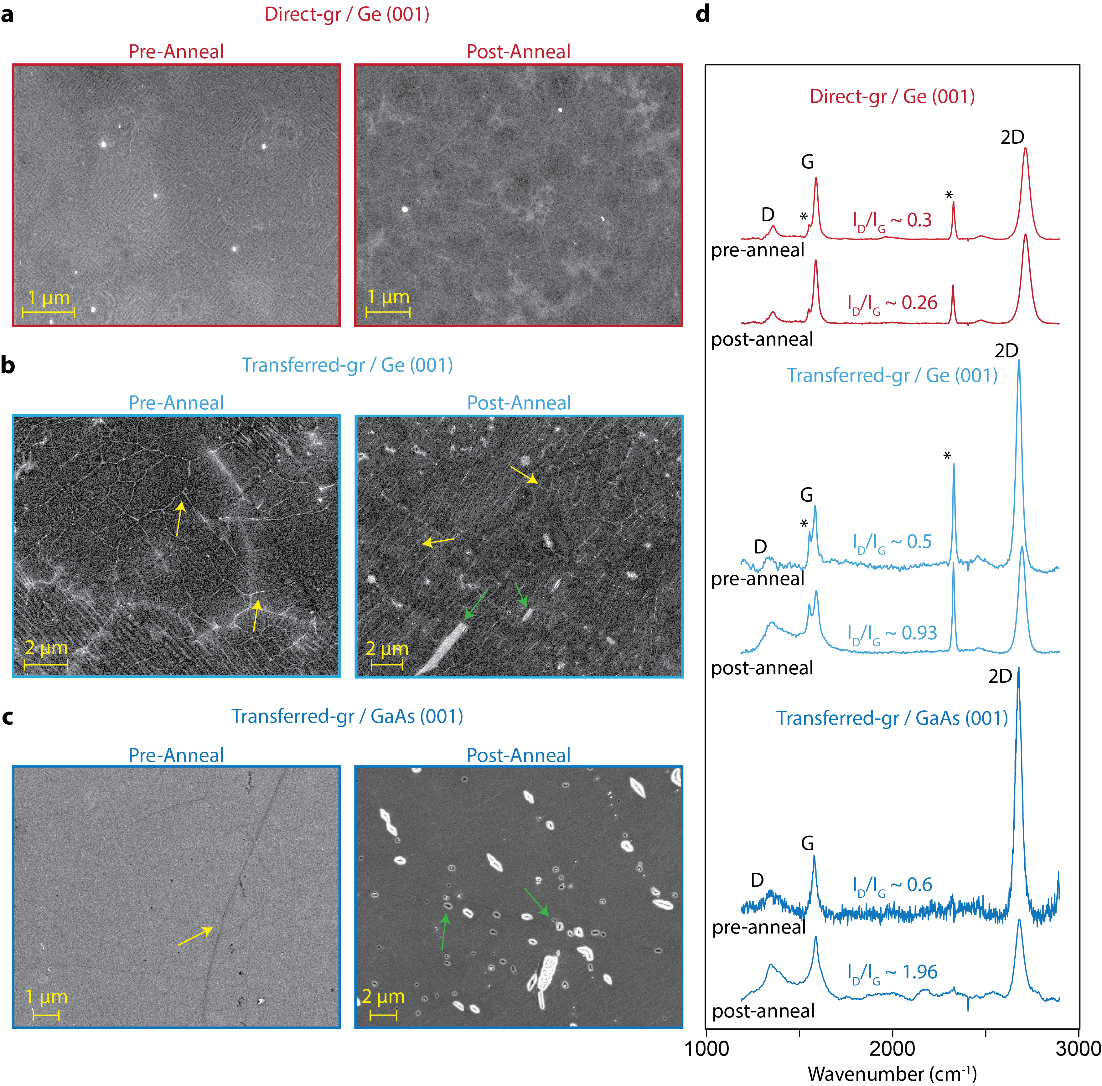
Fig. 1 illustrates the differences between the directly-grown graphene versus graphene that has been layer transferred onto Ge. We first examine the samples after light outgassing at C to remove solvents and adsorbates, but before full annealing (labelled “pre-anneal”, Fig. 1). For direct-growth graphene on Ge, the primary feature observed by scanning electron microscopy (SEM) is faceting of the Ge (001) surface (Fig. 1a, left), as has been observed previously 17. In contrast, the layer-transferred graphene on Ge displays a network of grain boundaries and wrinkles as labelled by the yellow arrows (Fig. 1b, left). The grain boundaries originate from graphene growth on polycrystalline Cu foils (Supporting Information Fig. LABEL:sm_cufoilSEM). Atomic force microscopy (AFM) measurements confirm the grain boundaries and wrinkles for transferred graphene (Fig. LABEL:sm_afmb, left). Neither layer transferred nor directly grown graphene show obvious signs of holes or tears prior to annealing in SEM or AFM measurements. Raman spectroscopy (Fig. 1d) shows the integrated intensity ratio for the direct and layer transferred graphene on Ge before anneal are similar (0.3 and 0.5, respectively), indicative of a similar defect density 18, 19. Layer-transferred graphene on GaAs (001) exhibits qualitatively similar surface morphology and Raman spectra as the graphene transferred onto Ge (001) (Fig. 1c, left).
After annealing in ultrahigh vacuum at 600∘C, which is necessary to remove substrate native oxides prior to film deposition 20, 21, we observe stark contrast between the two different graphene preparations. For directly grown graphene on Ge, our Raman, SEM, and AFM measurements display negligible differences before and after annealing (Fig. 1a, right). AFM measurements reveal faint wrinkles in the graphene layer formed after annealing (Supporting Information Fig. LABEL:sm_afm), but no obvious formation of tears (Fig. 1a) and negligible changes in the Raman ratio (Fig. 1d, red curves). In contrast, for layer-transferred graphene our SEM and AFM measurements reveal holes and tears that appear to originate at grain boundaries (green arrows in Fig. 1b (right) and Supporting Information Fig. LABEL:sm_afm). This increase in defect density is further confirmed through Raman spectroscopy, where we observe a dramatic increase in the Raman ratio for transferred graphene after annealing (Fig. 1d, blue curves), indicating the creation of tears and other defects. We observe a similar increase in the tear density and Raman ratio for transferred graphene on GaAs after annealing (Fig. 1c).
We hypothesize that the anneal-induced tears are created by desorption of native oxides that are trapped between the substrate and layer transferred graphene. Previous in-situ XPS measurements demonstrate that layer transferred graphene on III-V substrates contains oxides trapped at the graphene/III-V interface 22. Desorption of these interfacial oxides creates pinholes in the graphene. We expect transferred graphene/Ge to behave similarly. In contrast, graphene that is directly grown on Ge does not have these interfacial contaminants, and thus does not show an increased defect density after annealing.
We now measure the diffusion barrier performance for Mn thin films grown on the above graphene-terminated samples. After loading the graphene/Ge samples into vacuum and annealing at 600 C, Mn thin films ( atoms/cm2, Å) were grown by molecular beam epitaxy (MBE) at room temperature. After growth, samples were transferred via an ultrahigh vacuum manifold to a connected X-ray photoemission spectroscopy (XPS) chamber. In this way, we measure clean XPS spectra of samples that have not been exposed to air. Further details are described in Methods.
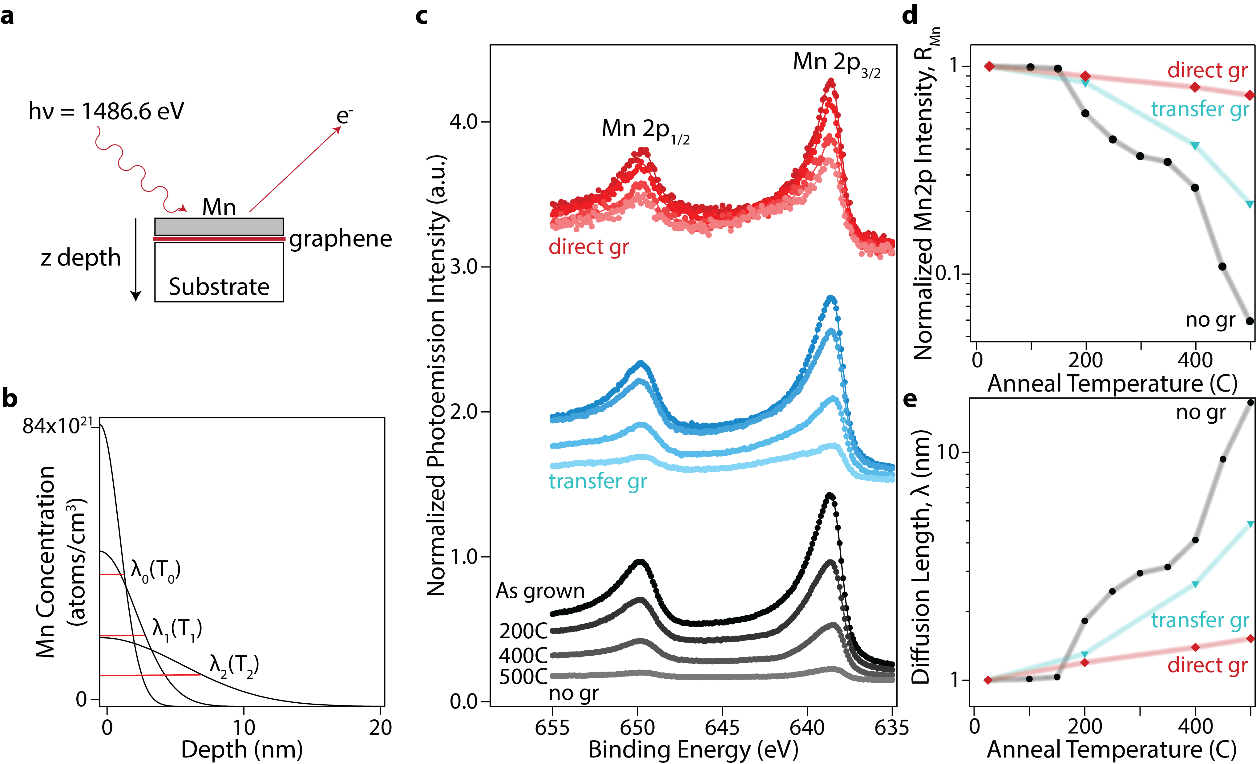
Figure 2c presents in-situ photoemission spectra tracking the evolution of Mn surface composition for Mn films grown on Ge substrates, with and without a graphene barrier. Each sample was subjected to a series of anneal steps at increasing temperature up to 500 ∘C. To eliminate variations in sample alignment, all spectra are normalized to the integrated Ge core level intensity. For the Mn film grown directly on Ge (black curves), with increasing anneal temperature the intensity of the Mn rapidly decreases, corresponding to a decrease in the relative surface Mn composition. For Mn on transferred graphene (blue curves) and on direct-growth graphene (red curves), the Mn core level decay is suppressed.
To compare the relative changes in surface Mn concentration, we fit the Mn and Ge core levels to Doniach-Sunjic 23 and Voigt lineshapes, respectively, and plot the relative change in Mn / Ge intensity ratio, (Fig. 2d, Ge ). Here the numerator with subscript refers to the Mn / Ge intensity ratio after anneal at temperature and the denominator with subscript refers to the Mn / Ge intensity ratio as-grown, before additional annealing. This normalization procedure cancels out the instrumental sensitivity, alignment, and photoemission cross section.
We find that the directly-grown graphene performs best as a diffusion barrier, with decreasing to only 0.7 after an anneal up to 500∘C, compared to for the sample without graphene. Transferred graphene also suppresses interdiffusion compared to the bare substrate. For the no graphene sample there is a distinct onset of interdiffusion around 150∘C, at which point rapidly decreases. There is no distinct onset for the samples with graphene barriers. Together, these results demonstrate that both transferred and directly-grown graphene are effective solid state diffusion barriers for Mn in Ge, and that directly-grown graphene is most effective.
We next estimate the temperature-dependent diffusion length based on the relative changes in the Mn / Ge intensity ratio, . For a very thin Mn film on a semi-infinite substrate, the solution to the diffusion equation is a half Gaussian composition profile (Fig. 2b)
| (1) |
where is the diffusion length and atoms/cm2 is the total areal density of Mn deposited. We define the as-deposited initial condition such that the Mn concentration at the surface () is equal to the density of pure Mn, i.e. atoms/cm3. This yields an initial diffusion length of Å. For simplicity, we let the Ge composition profile be , assuming that pure Mn, pure Ge, and the diffused Mn-Ge have approximately the same atomic densities and layer spacings.
From these composition profiles we calculate the expected intensity ratios for Mn 2p and Ge 3p, as a function of the diffusion length. The intensity of core level is given by
| (2) |
where is the two-dimensional density of atomic layer , is the depth from the surface, is the inelastic mean free path (20 Å for Mn , 26 Å for Ge , 22.1 Å for Ga 24), is the emission angle from surface normal, is an instrument sensitivity factor, and is the photoemission cross section. We rewrite the composition profiles in terms of atomic density, , where is the atomic layer spacing, and calculate the photoemission intensities and , subject to the initial condition Å. We then compute the normalized Mn intensity ratio , such that and are cancelled out. In this way, the experimentally measured is uniquely defined by the diffusion length after each sequential anneal.
Fig. 2(e) shows the estimated diffusion length, obtained by fitting the experimentally measured to the calculated intensity ratios from Eqs 1 and 2. We find that compared to the bare Ge substrate, directly-grown graphene on Ge suppresses the diffusion length by a factor of just under 11 and layer transferred graphene suppresses the diffusion length by a factor 3.5, at a temperature of 500 ∘C.
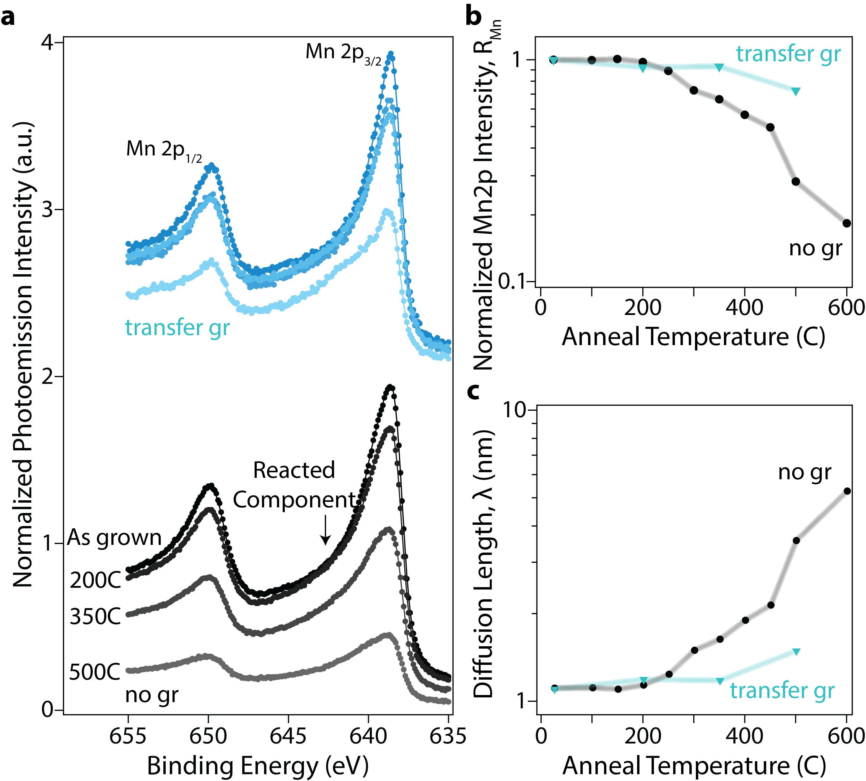
In-situ photoemission measurements for Mn on GaAs substrates reveal similar behavior as the samples on Ge (Fig. 3). For the Mn directly on GaAs (Fig. 3a, black curves), in the as-grown spectrum we observe a secondary component at higher binding energy, indicative of reactions or secondary phases between Mn and GaAs. This reacted component grows with increased annealing. We attribute these secondary components to the formation of Mn2As and MnGa phases, as has been observed previously at Mn/GaAs interfaces without graphene 25. Comparison of the normalized Mn 2p intensity and the estimated diffusion length reveal that like Ge, transferred graphene suppresses interdiffusion into GaAs.
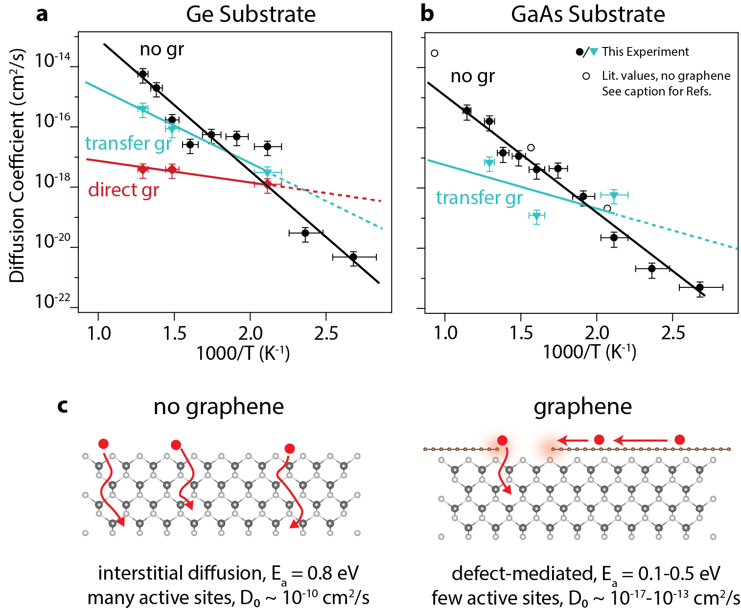
We now use the diffusion length to estimate the diffusivity via . Since each sample is subjected to a series of anneals at increasing temperature, we approximate the cumulative diffusion length squared after anneal steps as a sum of the previous diffusion steps
| (3) |
where is the time increment of anneal step and is the diffusivity from the anneal at temperature . Since each anneal is for a constant amount of time ( 5 minutes), we rewrite Equation 3 to solve for contribution of an individual anneal step.
| (4) |
We plot the diffusivity as a function of temperature in Fig. 4. From an Arrhenius fit, , we extract activation energies and diffusivity prefactors as listed in Table I. We find that at 500 ∘C, the diffusivity for Mn on directly-grown graphene / Ge (red curve) is a factor of 1000 lower than the diffusivity on bare Ge (black curve). Mn on transferred graphene / Ge is only a factor of 10 lower (blue curve). Similar behavior is observed for transferred graphene/GaAs compared to bare GaAs. To benchmark the accuracy of our method, we find that our experimentally determined diffusivities for Mn on bare GaAs (Fig. 4(b), filled black circles) are in good agreement with previous experiments (open black circles) 26, 27, 28.
| (cm2/s) | (eV) | C) (cm2/s) | ||
| post-anneal | ||||
| Ge | – | 0.81 | ||
| transfer gr/Ge | 0.93 | 0.50 | ||
| direct-growth gr/Ge | 0.26 | 0.13 | ||
| GaAs | – | 0.79 | ||
| transfer gr/GaAs | 1.96 | 0.21 |
.
We now discuss the mechanisms for Mn diffusion based on the experimentally determined and . Our experimentally determined activation energy of 0.8 eV for Mn diffusing into bare GaAs and Ge agrees well with previous experiments and DFT calculations for Mn interstitial diffusion into GaAs ( eV 29). Substitutional diffusion is expected to exhibit a higher activation energy of 2-3 eV 30.
In comparison, for Mn diffusion into graphene-terminated substrates is considerably lower: 0.1 eV for directly-grown graphene on Ge, and 0.2-0.5 eV for transferred graphene on GaAs and Ge. We immediately rule out transverse diffusion through pristine graphene, since diffusion through graphene in the absence of defects is expected to have a very large activation energy barrier of eV 31. This is because the effective pore size of graphene is small ( Å radius of a carbon ring, less than half the radius of a Mn atom). Therefore, we expect that Mn diffusion through graphene occurs primarily through defect-mediated processes.
The range of measured activation energies suggests several mechanisms for Mn diffusion through graphene defects may be possible. At high temperatures ( C, or K-1), we speculate that our extracted is lower on graphene-terminated substrates than on bare substrates due to reactions being catalyzed at graphene defects, since graphene defects are known to be chemically active 2, 32. At this point we do not have sufficient data to determine the mechanisms of diffusion lower temperatures, C (or K-1, Fig. 4 dotted lines). The range of measured activation energies may also reflect a convolution of surface and bulk diffusion, in which Mn adatoms first diffuse laterally to reactive pinhole sites before then diffusing into the substrate (Fig. 4c). First-principles calculations suggest that the activation energy for lateral diffusion of Mn on graphene is 60 meV 33 and Cu on graphene is 10-20 meV 34, similar to the activation energies extracted from our photoemission measurements (Table 1). More detailed experiments with lateral and depth resolution, at a broader range of temperatures, are needed to fully understand the detailed diffusion mechanisms through graphene.
While a low activation energy barrier favors a large diffusivity, the origin of the dramatic decrease of diffusivity for graphene-terminated samples is the reduction of the prefactor . We interpret to scale as an attempt rate for diffusion. For Mn on bare GaAs and Ge substrates, the attempt rates of cm2/s are high because there are many available sites for interstitial diffusion into the substrate. On the other hand, attempt rates are lower on the graphene-terminated substrates because Mn diffusion through graphene requires a defect in the graphene. This rate is higher for layer transferred graphene ( cm2/s) than for directly-grown graphene ( cm2/s), since the layer-transferred graphene has a higher defect density as quantified by our Raman, SEM, and AFM measurements (Fig. 1 and Supporting Information Fig. LABEL:sm_afm). Note that film/substrate interactions 35 and doping 36 can modify Raman intensity ratios 37, therefor it is difficult to make direct comparisons of gr/Ge and gr/GaAs defect densities based on the ratio (Fig. 1d). Further experiments are required to correlate specific defect types (e.g. tears, wrinkles, pinholes, vacancies) with specific values of the diffusivity.
4 Conclusions
Our results show that layer-transferred and directly-grown graphene suppress Mn diffusion into semiconductor substrates. The directly-grown graphene displays superior diffusion barrier performance due to a lower defect density, as quantified by Raman spectroscopy and SEM after annealing but before Mn film growth. Translating these performance enhancements to functional substrates at wafer scale will require direct graphene synthesis approaches on the substrate of interest. For example, CVD approaches using small molecules 38, activated precursors 39, or plasma-enhanced CVD processes 40, 41, 42 show promise for reducing the graphene synthesis temperature, and may be a route for graphene growth directly on GaAs and other technologically important compound semiconductors.
Supporting Information: SEM images of graphene grown on Cu foils; AFM measurements of directly grown graphene on Ge, transferred graphene on Ge, and transferred graphene on GaAs; and Raman fitting of the graphene and amorphous carbon peaks.
5 Acknowledgment
Mn film growth, graphene transfer, and photoemission experiments by PJS, SM, and JKK were primarily supported by the CAREER program National Science Foundation (DMR-1752797). In-situ photoemission experiments and analysis by PJS and JKK was partially supported by the NSF Division of Materials Research through the University of Wisconsin Materials Research Science and Engineering Center (Grant No. DMR-1720415). Graphene synthesis and characterization by VS, KS, and MSA are supported by the U.S. Department of Energy, Office of Science, Basic Energy Sciences, under award no. DE-SC0016007. We gratefully acknowledge the use of Raman and electron microscopy facilities supported by the NSF through the University of Wisconsin Materials Research Science and Engineering Center under Grant No. DMR-1720415.
6 References
References
- Topsakal et al. 2012 Topsakal, M.; Şahin, H.; Ciraci, S. Graphene Coatings: An Efficient Protection from Oxidation. Phys. Rev. B 2012, 85
- Roy and Arnold 2013 Roy, S. S.; Arnold, M. S. Improving Graphene Diffusion Barriers via Stacking Multiple Layers and Grain Size Engineering. Adv. Funct. Mater. 2013, 23, 3638–3644
- Hong et al. 2014 Hong, J.; Lee, S.; Lee, S.; Han, H.; Mahata, C.; Yeon, H.-W.; Koo, B.; Kim, S.-I.; Nam, T.; Byun, K.; Min, B.-W.; Kim, Y.-W.; Kim, H.; Joo, Y.-C.; Lee, T. Graphene as an Atomically Thin Barrier to Cu Diffusion into Si. Nanoscale 2014, 6, 7503–7511
- Cobas et al. 2012 Cobas, E.; Friedman, A. L.; van’t Erve, O. M.; Robinson, J. T.; Jonker, B. T. Graphene as a Tunnel Barrier: Graphene-based Magnetic Tunnel Junctions. Nano Lett. 2012, 12, 3000–3004
- Lu et al. 2018 Lu, Z.; Sun, X.; Xie, W.; Littlejohn, A.; Wang, G.-C.; Zhang, S.; Washington, M. A.; Lu, T.-M. Remote Epitaxy of Copper on Sapphire through Monolayer Graphene Buffer. Nanotechnology 2018, 29, 445702
- Kim et al. 2017 Kim, Y.; Cruz, S. S.; Lee, K.; Alawode, B. O.; Choi, C.; Song, Y.; Johnson, J. M.; Heidelberger, C.; Kong, W.; Choi, S.; Qiao, K.; Almansouri, I.; Fitzgerald, E. A.; Kong, J.; Kolpak, A. M.; Hwang, J.; Kim, J. Remote Epitaxy through Graphene Enables Two-Dimensional Material-based Layer Transfer. Nature 2017, 544, 340–343
- Du et al. 2021 Du, D.; Manzo, S.; Zhang, C.; Saraswat, V.; Genser, K. T.; Rabe, K. M.; Voyles, P. M.; Arnold, M. S.; Kawasaki, J. K. Epitaxy, Exfoliation, and Strain-Induced Magnetism in Rippled Heusler Membranes. Nat. Commun. 2021, 12, 2494
- Sands et al. 1990 Sands, T.; Palmstrøm, C.; Harbison, J.; Keramidas, V.; Tabatabaie, N.; Cheeks, T.; Ramesh, R.; Silberberg, Y. Stable and Epitaxial Metal/III-V Semiconductor Heterostructures. Materials Science Reports 1990, 5, 99–170
- Ma et al. 2019 Ma, L.-P.; Ren, W.; Cheng, H.-M. Transfer Methods of Graphene from Metal Substrates: A Review. Small Methods 2019, 3, 1900049
- Oh et al. 2015 Oh, S.; Jung, Y.; Kim, J. Effects of Defect Density on Ultrathin Graphene-based Metal Diffusion Barriers. J. Vac. Sci. Technol. 2015, 33, 061510
- Yuan et al. 2013 Yuan, J.; Ma, L.-P.; Pei, S.; Du, J.; Su, Y.; Ren, W.; Cheng, H.-M. Tuning the Electrical and Optical Properties of Graphene by Ozone Treatment for Patterning Monolithic Transparent Electrodes. ACS Nano 2013, 7, 4233–4241
- Farshchi and Ramsteiner 2013 Farshchi, R.; Ramsteiner, M. Spin Injection from Heusler Alloys into Semiconductors: A Materials Perspective. J. Appl. Phys. 2013, 113, 191101
- Dong et al. 2005 Dong, X.; Adelmann, C.; Xie, J.; Palmstrøm, C.; Lou, X.; Strand, J.; Crowell, P.; Barnes, J.-P.; Petford-Long, A. Spin Injection from the Heusler Alloy Co2MnGe into Al0.1Ga0.9As/ GaAs Heterostructures. Appl. Phys. Lett. 2005, 86, 102107
- Kiraly et al. 2015 Kiraly, B.; Jacobberger, R. M.; Mannix, A. J.; Campbell, G. P.; Bedzyk, M. J.; Arnold, M. S.; Hersam, M. C.; Guisinger, N. P. Electronic and Mechanical Properties of Graphene-Germanium Interfaces Grown by Chemical Vapor Deposition. Nano Lett. 2015, 15, 7414–7420
- Wang et al. 2013 Wang, G.; Zhang, M.; Zhu, Y.; Ding, G.; Jiang, D.; Qinglei, G.; Liu, S.; Xie, X.; Chu, P. K.; Di, Z.; Wang, X. Direct Growth of Graphene Film on Germanium Substrate. Sci. Rep. 2013, 3, 2465
- Park et al. 2018 Park, H.; Lim, C.; Lee, C.-J.; Kang, J.; Kim, J.; Choi, M.; Park, H. Optimized Poly(Methyl Methacrylate)-Mediated Graphene-Transfer Process for Fabrication of High-Quality Graphene Layer. Nanotechnology 2018, 29, 415303
- McElhinny et al. 2016 McElhinny, K. M.; Jacobberger, R. M.; Zaug, A. J.; Arnold, M. S.; Evans, P. G. Graphene-induced Ge (001) surface faceting. Surface Science 2016, 647, 90–95
- Tuinstra and Koenig 1970 Tuinstra, F.; Koenig, J. L. Raman spectrum of graphite. The Journal of chemical physics 1970, 53, 1126–1130
- Cançado et al. 2011 Cançado, L. G.; Jorio, A.; Martins Ferreira, E. H.; Stavale, F.; Achete, C. A.; Capaz, R. B.; Moutinho, M. V. O.; Lombardo, A.; Kulmala, T. S.; Ferrari, A. C. Quantifying Defects in Graphene via Raman Spectroscopy at Different Excitation Energies. Nano Lett. 2011, 11, 3190–3196
- SpringThorpe et al. 1987 SpringThorpe, A.; Ingrey, S.; Emmerstorfer, B.; Mandeville, P.; Moore, W. Measurement of GaAs surface oxide desorption temperatures. Applied physics letters 1987, 50, 77–79
- Oh and Campbell 2004 Oh, J.; Campbell, J. C. Thermal desorption of Ge native oxides and the loss of Ge from the surface. Journal of electronic materials 2004, 33, 364–367
- Manzo et al. 2021 Manzo, S.; Strohbeen, P. J.; Lim, Z.-H.; Saraswat, V.; Arnold, M. S.; Kawasaki, J. K. Defect-seeded lateral epitaxy and exfoliation on graphene-terminated surfaces. arXiv preprint arXiv:2106.00721 2021,
- Doniach and Sunjic 1970 Doniach, S.; Sunjic, M. Many-Electron Singularity in X-ray Photoemission and X-ray Line Spectra from Metals. J. Phys. C: Solid State Phys. 1970, 3, 285–291
- Tanuma et al. 2003 Tanuma, S.; Powell, C. J.; Penn, D. R. Calculation of electron inelastic mean free paths (IMFPs) VII. Reliability of the TPP-2M IMFP predictive equation. Surf. Interface Anal. 2003, 35, 268–275
- Hilton et al. 2004 Hilton, J. L.; Schultz, B. D.; McKernan, S.; Palmstrøm, C. J. Interfacial Reactions of Mn/GaAs Thin Films. Appl. Phys. Lett. 2004, 84, 3145–3147
- Seltzer 1965 Seltzer, M. S. Diffusion of Manganese into Gallium Arsenide. J. Phys. Chem. Solids 1965, 26, 243–250
- Adell et al. 2011 Adell, J.; Ulfat, I.; Ilver, L.; Sadowski, J.; Karlsson, K.; Kanski, J. Thermal Diffusion of Mn through GaAs Overlayers on (Ga,Mn)As. J. Phys.: Condens. Matter 2011, 23, 085003
- Vikhrova et al. 2012 Vikhrova, O. V.; Danilov, Y. A.; Drozdov, M. N.; Zvonkov, B. N.; Kalent’eva, I. L. Manganese Diffusion in InGaAs/GaAs Quantum Well Structures. J. Synch. Investig. 2012, 6, 508–510
- Edmonds et al. 2004 Edmonds, K. W.; Boguslawski, P.; Wang, K. Y.; Campion, R. P.; Novikov, S. N.; Farley, N. R. S.; Gallagher, B. L.; Foxon, C. T.; Sawicki, M.; Dietl, T.; Buongiorno Nardelli, M.; Bernholc, J. Mn Interstitial Diffusion in (Ga,Mn)As. Phys. Rev. Lett. 2004, 92, 037201
- Raebiger et al. 2006 Raebiger, H.; Ganchenkova, M.; von Boehm, J. Diffusion and Clustering of Substitutional Mn in (Ga,Mn)As. Appl. Phys. Lett. 2006, 89, 012505
- Leenaerts et al. 2008 Leenaerts, O.; Parteons, B.; Peeters, F. M. Graphene: A Perfect Nanoballoon. Appl. Phys. Lett. 2008, 93, 193107
- Yoon et al. 2014 Yoon, T.; Mun, J. H.; Cho, B. J.; Kim, T.-S. Penetration and Lateral Diffusion Characteristics of Polycrystalline Graphene Barriers. Nanoscale 2014, 6, 151–156
- Liu and Wang 2016 Liu, X.; Wang, C.-Z. Growth mode and structures of magnetic Mn clusters on graphene. RSC advances 2016, 6, 64595–64604
- Han et al. 2019 Han, Y.; Lii-Rosales, A.; Tringides, M. C.; Evans, J. W.; Thiel, P. A. Energetics of Cu adsorption and intercalation at graphite step edges. Physical Review B 2019, 99, 115415
- Obraztsov et al. 2008 Obraztsov, A. N.; Tyurnina, A. V.; Obraztsova, E. A.; Zolotukhin, A. A.; Liu, B.; Chin, K.-C.; Wee, A. T. Raman scattering characterization of CVD graphite films. Carbon 2008, 46, 963–968
- Das et al. 2008 Das, A.; Pisana, S.; Chakraborty, B.; Piscanec, S.; Saha, S. K.; Waghmare, U. V.; Novoselov, K. S.; Krishnamurthy, H. R.; Geim, A. K.; Ferrari, A. C., et al. Monitoring dopants by Raman scattering in an electrochemically top-gated graphene transistor. Nature nanotechnology 2008, 3, 210–215
- Ferralis 2010 Ferralis, N. Probing mechanical properties of graphene with Raman spectroscopy. Journal of materials science 2010, 45, 5135–5149
- Li et al. 2011 Li, Z.; Wu, P.; Wang, C.; Fan, X.; Zhang, W.; Zhai, X.; Zeng, C.; Li, Z.; Yang, J.; Hou, J. Low-Temperature Growth of Graphene by Chemical Vapor Deposition using Solid and Liquid Carbon Sources. ACS Nano 2011, 5, 3385–3390
- Lee et al. 2010 Lee, S.; Toney, M. F.; Ko, W.; Randel, J. C.; Jung, H. J.; Munakata, K.; Lu, J.; Geballe, T. H.; Beasley, M. R.; Sinclair, R.; Manoharan, H. C.; Salleo, A. Laser-Synthesized Epitaxial Graphene. ACS Nano 2010, 4, 7524–7530
- Vishwakarma et al. 2019 Vishwakarma, R.; Zhu, R.; Abuelwafa, A. A.; Mabuchi, Y.; Adhikari, S.; Ichimura, S.; Soga, T.; Umeno, M. Direct Synthesis of Large-Area Graphene on Insulating Substrates at Low Temperature using Microwave Plasma CVD. ACS Omega 2019, 4, 11263–11270
- Mischke et al. 2020 Mischke, J.; Pennings, J.; Weisenseel, E.; Kerger, P.; Rohwerder, M.; Mertin, W.; Bacher, G. Direct Growth of Graphene on GaN via Plasma-Enhanced Chemical Vapor Deposition under Atmosphere. 2D Mater. 2020, 7, 035019
- Li et al. 2021 Li, N.; Zhen, Z.; Zhang, R.; Xu, Z.; Zheng, Z.; He, L. Nucleation and Growth Dynamics of Graphene Grown by Radio Frequency Plasma-Enhanced Chemical Vapor Deposition. Sci. Rep. 2021, 11, 6007