On MOSFET Threshold Voltage Extraction Over the Full Range of Drain Voltage Based on Gm/ID
Abstract
A MOSFET threshold voltage extraction method covering the entire range of drain-to-source voltage, from linear to saturation modes, is presented. Transconductance-to-current ratio is obtained from MOSFET transfer characteristics measured at low to high drain voltage. Based on the charge-based modeling approach, a near-constant value of threshold voltage is obtained over the whole range of drain voltage for ideal, long-channel MOSFETs. The method reveals a distinct increase of threshold voltage versus drain voltage for halo-implanted MOSFETs in the low drain voltage range. The method benefits from moderate inversion operation, where high-field effects, such as vertical field mobility reduction and series resistances, are minimal. The present method is applicable over the full range of drain voltage, is fully analytical, easy to be implemented, and provides more consistent results when compared to existing methods.
Index Terms:
Halo implant, Long-channel DIBL, MOSFET, Threshold voltage, Transconductance-to-current ratio.I Introduction
Threshold voltage extraction methods for MOSFETs that cover the full range of drain voltage are rare, mainly due to the regional approaches underlying many conventional methods [1]. Moderate inversion in MOSFETs, where diffusion and drift transport components have comparable magnitude, covers an important range of current. The recognition that has a quite universal behavior over technology, bias ranges (mostly in saturation), and temperature [2], [3], enhances the interest in related techniques. The transconductance-to-current ratio change (cTCR) methods relate the extremum of to threshold voltage in [4], [5], [6] and may be applied from linear to saturation operation. A drawback of these methods is the increased noise due to the necessary successive derivations. Methods relying directly on transconductance-to-current ratio [7], [8] emphasize on linear mode operation. The adjusted constant-current (ACC) [9] and generalized constant-current (GCC) [10] techniques relate a threshold current criterion directly to . The ACC method is applicable over the full range of drain voltage [9]. All the aforementioned methods relate to and hence share a sound physical basis. None of them, to the best of our knowledge, has been demonstrated in detail over the full range of drain voltage.
A novel, simple, and fully analytic method of threshold voltage extraction based on transconductance-to-current ratio (TCR) is introduced in this work. The latter is obtained from measured at different values of . The method is based on the theory of the charge-based model [11], [12]. While formally equivalent to the ACC [9] method, the usage of the Lambert W function renders the procedure analytically explicit. The method is among the few with which threshold voltage may be consistently obtained over the whole range of drain voltage, from linear mode to saturation. The method is shown to yield a threshold voltage independent of drain voltage for ideal long-channel MOSFETs. For halo-doped MOSFETs, the method reveals a characteristic increase of threshold voltage at . The method is particularly suited for the investigation of DIBL effects including long-channel DIBL [13].
II MOSFET Threshold Voltage Extraction Method for Full Drain Voltage Range
The charge-voltage relation in a long-channel MOSFET is given in [11] as,
| (1) |
where are the pinch-off, gate, source and drain voltages (all referred to local substrate), and thermal voltage is . The pinch-off voltage is estimated as in [9],
| (2) |
where and is the threshold voltage and slope factor, respectively. are the normalized mobile charge densities at source and drain sides [9], respectively. Solving for mobile charges results in,
| (3) |
where is the Lambert W (product logarithm) function. An analytical approximation with sufficient accuracy is [14]
.
Using the definition of threshold voltage in [9], [10] whereas threshold voltage is defined as the gate voltage for which the minimum potential in the channel () becomes equal to the pinch-off voltage . Utilizing in (3) gives,
| (4) |
where . Using the general charge-based expression for the transconductance-to-current ratio for MOSFETs,
| (5) |
where is the weak inversion slope factor, evaluated from in weak inversion. Utilizing (4) we obtain at threshold,
| (6) |
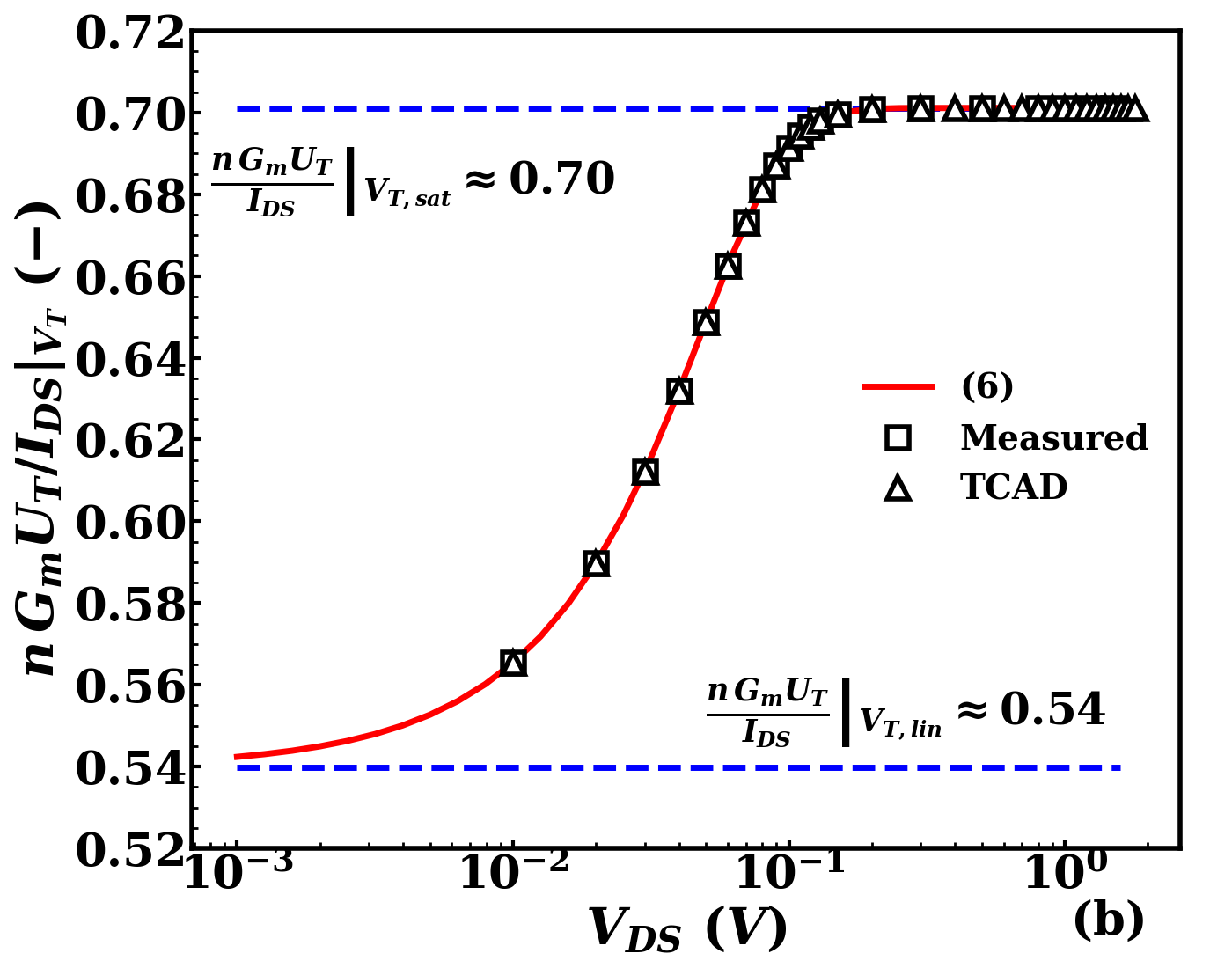
Hence (6) provides an explicit, analytical criterion to determine threshold voltage over the full range of , that does not require any numerical iterations. In particular, for in linear region (6) gives ,
| (7) |
while for saturation, ,
| (8) |
Hence, the threshold voltage is determined as the gate voltage at which corresponds to a certain fraction of its maximum value in weak inversion, depending solely on . The extraction takes place in moderate inversion so series resistance and mobility degradation have minimum effect on extracted threshold voltage.
III Experiment and Discussion
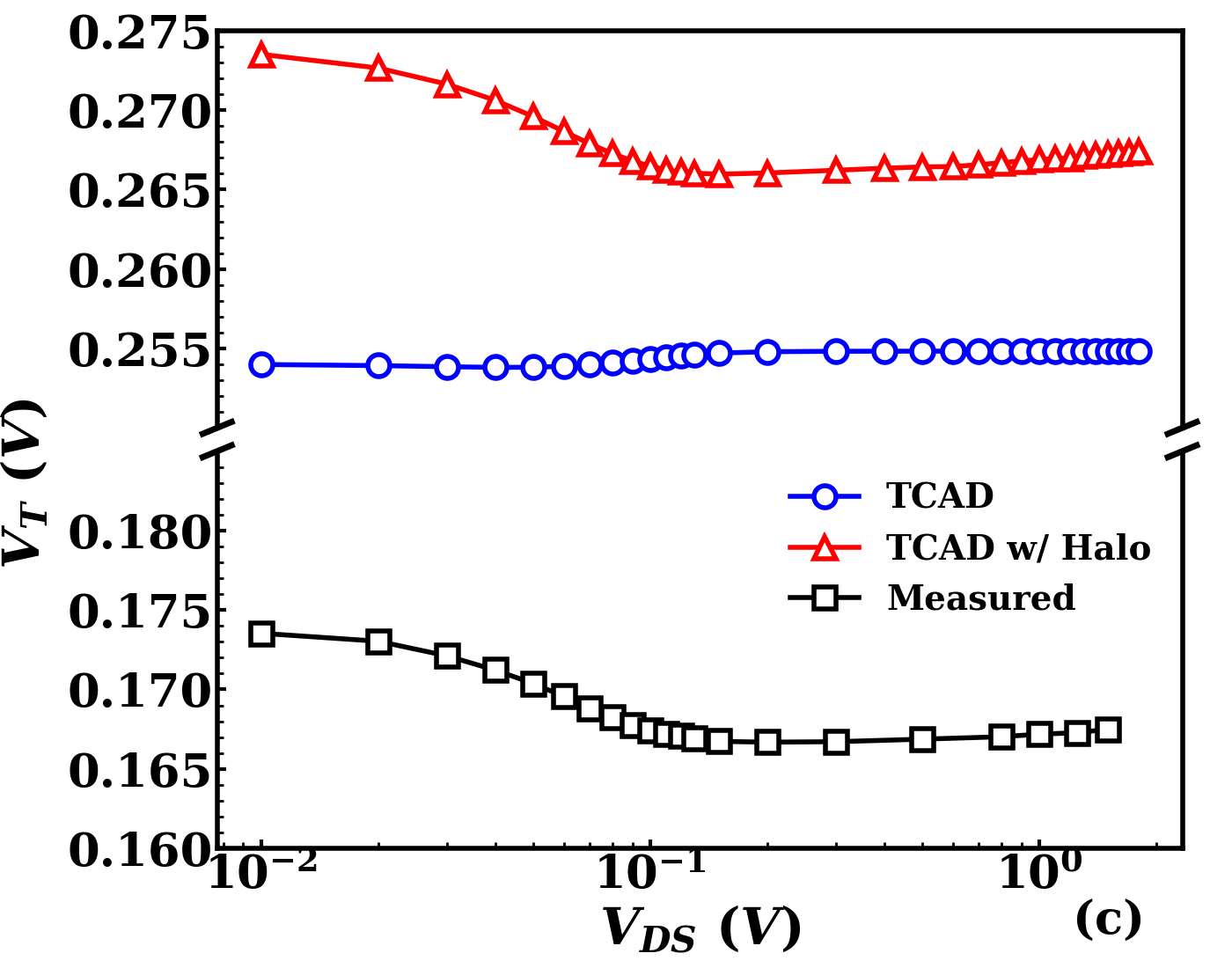
To validate our method, TCAD simulation and measurements are utilized. A long-channel () NMOS device with oxide thickness and uniform substrate doping was simulated with Silvaco Atlas, at room temperature, using CVT mobility and Shockley-Read-Hall (SRH) recombination models. Two cases without and with pocket/halo implants are considered, where the halo implants are uniformly doped areas () placed below drain and source extensions.
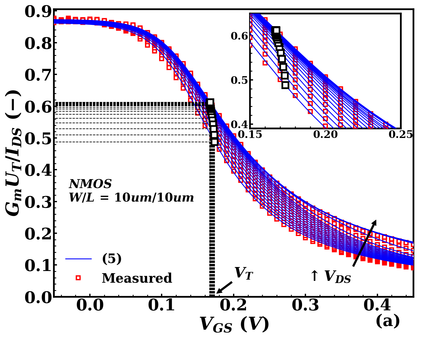
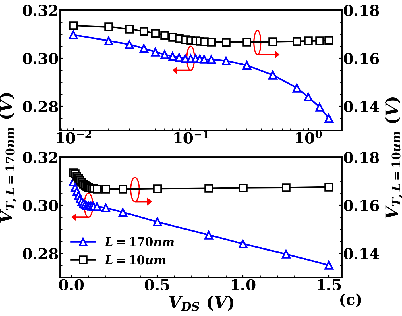
Transconductance-to-current ratio for the whole range of drain voltage, from to , measured from a long-channel () NMOS transistor of a CMOS technology is shown in Fig. 1(a). To confirm that the extracted is compatible with the used charge-based approach, is evaluated from (5) and demonstrated in Fig.1(a). The normalized charges and in (5) are calculated using (3) where is evaluated from (2) using the extracted values of and . The model fits measured characteristics adequately, confirming the consistency of procedure and model. The transconductance-to current-ratio which corresponds to vs. and its asymptotic behavior in linear and saturation modes according to (7) and (8) is shown in Fig. 1(b). The extracted threshold voltage vs. is shown in Fig. 1(c). The latter also shows results of TCAD simulations. The case without halo implant features an almost invariable threshold voltage [9], within . The case with halo implant shows a characteristic increase of at when the device is in non-saturation. The same qualitative increase observed in the real device may therefore clearly be attributed to halo implant.
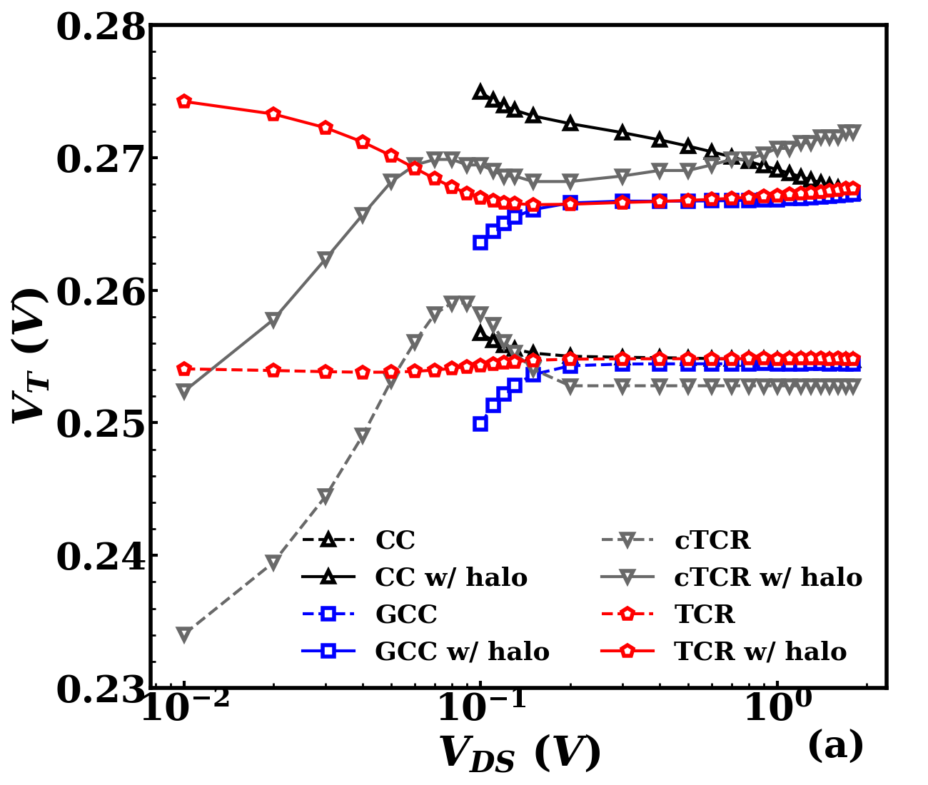
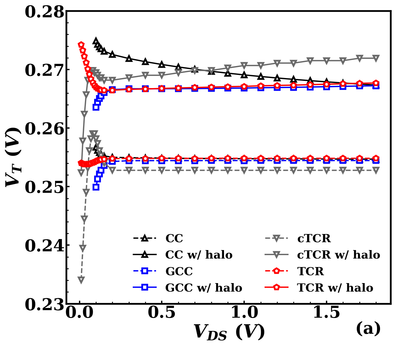
Extraction methods are compared in Fig. 2(a)-(b) for the long-channel TCAD-simulated device with and without halo implant. For the CC method used here, the current criterion to extract is with technology current in halo (non-halo) cases. is the specific current obtained as in [9]. For the GCC method, the threshold criterion is determined as , corresponding to an inversion coefficient i.e. [10]. The procedure is repeated for each value of . Both CC and GCC methods are implemented for saturation conditions (i.e. in moderate inversion). In the cTCR [5] method, is the gate voltage corresponding to the peak of . To obtain the needed resolution, we use a polynomial fitting of the data near the peak. The cTCR and this work’s TCR methods provide in the full range of . The different behavior of the extracted threshold voltage is immediately apparent. For the non-halo device, shows variation when departing from saturation, compared to the almost constant , while the CC and GCC methods in saturation yield practically the same as cTCR and TCR methods (to within ). For the case with halo implants, the different behavior becomes more apparent due to the nature of each method. A common point to CC, GCC and TCR methods is the same estimation of change in at highest among halo and non-halo cases.
In Fig. 2(c), the data of the long-channel device of Fig. 1 are compared to a short-channel device of the same CMOS process. The short-channel device shows the same qualitative increase of at low , while exhibiting a clear drain-induced barrier lowering (DIBL) at higher .
The present method is applicable to a wide range of purposes, from process characterization to extraction of parameters in charge-based compact models, such as EKV [15], ACM [16], or BSIM-bulk [17] models, but may be easily adapted for use in other compact models. The method is based on the characteristic in moderate inversion, which is universal in many ways among different geometry, device types, temperature, and to some extent even for different types of FETs. A distinct feature is its applicability over the full range of combined with moderate inversion operation, making it highly suitable for the investigation of DIBL and long-channel DIBL [13] effects.
IV Conclusion
A novel, fully analytical method for the extraction of threshold voltage in bulk MOSFETs over the full range of drain voltage has been presented. The method is based on the transconductance-to-current ratio in moderate inversion, and hence benefits from a low impact of high-field effects and series resistance. The charge-based modeling approach provides an explicit criterion for extracting directly from consistently for all . A practically constant value of threshold voltage is obtained in the full range of from linear to saturation modes for ideal, long-channel devices. Halo-implanted devices show a characteristic increase of threshold voltage at low drain voltage, which is attributed to pocket/halo doping. The method is furthermore applicable to investigate DIBL effects.
References
- [1] A. Ortiz-Conde, F. J. García-Sánchez, J. Muci, A. Terán Barrios, J. J. Liou and C.-S. Ho, “Revisiting MOSFET threshold voltage extraction methods”, Microelectron. Reliab., vol. 53, no. 1, pp. 90–104, 2013. doi: 10.1016/j.microrel.2012.09.015.
- [2] S. El Ghouli, D. Rideau, F. Monsieur, P. Scheer, G. Gouget, A. Juge, T. Poiroux, J.-M. Sallese and C. Lallement, ”Experimental gm/ID Invariance Assessment for Asymmetric Double-Gate FDSOI MOSFET,” IEEE Trans. Electron Devices, vol. 65, no. 1, pp. 11-18, Jan. 2018. doi: 10.1109/TED.2017.2772804.
- [3] J. R. R. De Oliveira Martins, A. Mostafa, J. Juillard, R. Hamani, F. De Oliveira Alves and P. Maris Ferreira, ”A Temperature-Aware Framework on gm/ID-Based Methodology Using 180 nm SOI From -40 °C to 200 °C,” IEEE Open Journal of Circuits and Systems, vol. 2, pp. 311-322, 2021. doi: 10.1109/OJCAS.2021.3067377.
- [4] K. Aoyama, ”A method for extracting the threshold voltage of MOSFETs based on current components,” in H. Ryssel, P. Pichler (Eds.) Simulation of Semiconductor Devices and Processes, pp. 118–121, Springer, Vienna, 1995. doi: 10.1007/978-3-7091-6619-2_28.
- [5] D. Flandre, V. Kilchytska, and T. Rudenko, “gm/Id Method for Threshold Voltage Extraction Applicable in Advanced MOSFETs With Nonlinear Behavior Above Threshold”, IEEE Electron Device Lett., vol. 31, no. 9, pp. 930-932, Sept. 2010. doi: 10.1109/LED.2010.2055829.
- [6] T. Rudenko et al., ”On the MOSFET threshold voltage extraction by transconductance and transconductance-to-current ratio change methods: Part II—Effect of drain voltage”, IEEE Trans. Electron Devices, vol. 58, no. 12, pp. 4180-4188, Dec. 2011. doi: 10.1109/TED.2011.2168227.
- [7] A. I. A. Cunha, M. C. Schneider, C Galup-Montoro, C. D. C. Caetano, and M. B. Machado, ”Unambiguous extraction of threshold voltage based on the transconductance-to-current ratio”, Workshop on Compact Models - NSTI Nanotech, pp. 139-142, 2005. [Online Available:] link.
- [8] O. F. Siebel, M. C. Schneider and C. Galup-Montoro, ”MOSFET threshold voltage: definition, extraction, and some applications”, Microelectron. J., vol. 43, no. 5, pp. 329–336, May 2012. doi: 10.1016/j.mejo.2012.01.004.
- [9] A. Bazigos, M. Bucher, J. Assenmacher, S. Decker et al., ”An adjusted constant-current method to determine saturated and linear mode threshold voltage of MOSFETs”, IEEE Trans. Electron Devices, vol. 58, no. 11, pp. 3751–3758, Nov. 2011. doi: 10.1109/TED.2011.2164080.
- [10] M. Bucher, N. Makris, L. Chevas, “Generalized Constant Current Method to Determine MOSFET Threshold Voltage”, IEEE Trans. Electron Devices, vol. 67, no. 11, pp. 4559-4562, Nov. 2020. doi: 10.1109/TED.2020.3019019.
- [11] J.-M. Sallese, M. Bucher, F. Krummenacher and P. Fazan, “Inversion charge linearization in MOSFET modeling and rigorous derivation of the EKV compact model”, Solid-State Electron., vol. 47, no. 4, pp. 677–683, 2003. doi: 10.1016/S0038-1101(02)00336-2.
- [12] C. Enz and E. Vittoz, Charge-based MOS transistor modeling, John Wiley and Sons, Chichester, 2006. doi: 10.1002/0470855460.
- [13] A. S. Roy, S. P. Mudanai, and M. Stettler, ”Mechanism of Long-Channel Drain-Induced Barrier Lowering in Halo MOSFETs”, IEEE Trans. Electron Devices, vol. 58, no. 4, pp. 979-984, Apr. 2011. doi: 10.1109/TED.2011.2109387.
- [14] S. Winitzki, ”Uniform Approximations for Transcendental Functions”, Computational Science and Its Applications (ICCSA), pp. 780-789, 2003. doi: 10.1007/3-540-44839-X_82
- [15] A. Bazigos, M. Bucher, F. Krummenacher, J.-M. Sallese et al., ”EKV3 compact MOSFET model documentation, model version 301.02“, Technical Report, Technical University of Crete, Chania, Greece, July 2008.
- [16] C. Galup-Montoro, M. C. Schneider, A. I. A. Cunha, F. Rangel de Sousa, H. Klimach and O. Franca Siebel, ”The Advanced Compact MOSFET (ACM) Model for Circuit Analysis and Design”, Proc. of IEEE Custom Integrated Circuits Conference, pp. 519-526, 2007. doi: 10.1109/CICC.2007.4405785.
- [17] H. Agarwal et al., ”Analytical Modeling and Experimental Validation of Threshold Voltage in BSIM6 MOSFET Model,” IEEE Journal of the Electron Devices Society, vol. 3, no. 3, pp. 240-243, May 2015. doi: 10.1109/JEDS.2015.2415584.