Phase stability in SmB6
Abstract
We investigate flux-grown Sm-deficient SmxB6 () by global and local tools, including X-ray diffraction (XRD), electronic transport, and scanning tunneling microscopy (STM) and spectroscopy (STS). All these tools indicate a remarkable persistence of the SmB6 local structure in the flux-grown samples even for nominal Sm concentrations as low as . As a consequence, the overall electronic properties of SmxB6, and particularly the surface conductance at low temperature, is only affected locally by the Sm-deficiency.
I Introduction
Materials that host topologically non-trivial surface states have recently become a topic of tremendous fundamental research interest [1] with potential device applications. Usually, topological insulators can be described by considering non-interacting electrons. However, as soon as electronic interactions become relevant, their description quickly turns into an often complex issue [2]. One of the most prominent examples here is the Kondo insulator SmB6 for which topologically non-trivial surface states have been proposed [3, 4]. This proposal was soon followed by an abundance of experimental studies (see e.g. Refs. 5, 6 for a review of the vast literature). The existence of conducting surface states is generally agreed upon by now [7, 8, 9, 10, 11, 12, 13]; however, the origin of these surface states is less clear-cut. Besides a topological nature [14, 15, 16, 17, 18], polarity-driven [19] or Rashba-split [20] surface states have been proposed, and issues related to bulk in-gap states and time-dependent surface states were discussed [19, 21, 22, 23]. Considering the relatively simple, cubic crystal structure (structure type CaB6, ), such complications came somewhat as a surprise. Yet, there are a number of issues [5] which indeed result in complex properties of SmB6: i) the most prominent surface, (100), is polar, ii) the Sm valence is intermediate ( at 300 K) and decreases slightly with decreasing temperature [24, 25], iii) a quartet ground state of the Sm configuration, is observed experimentally [26], in contrast with some band structure calculations [27, 28, 29].
Here, Scanning Tunneling Microscopy (STM) and Spectroscopy (STS) is well versed to investigate Kondo materials due to its capability to locally explore the surface structure and, in particular, the electronic Green’s function [30]. Consequently, a number of STM studies have been conducted [31, 10, 32, 33, 34, 17, 35, 18, 36, 37]; however, STM is also faced with issues mostly related to the difficulty to cleave SmB6 and the resulting scarcity of atomically flat surface areas which, in addition, exhibit a multitude of morphologies [38]. The assignment of some of these surfaces is disputed, which may have consequences for other surface sensitive measurements such as angle-resolved photoemission spectroscopy (ARPES).
To make progress here, we study nominally Sm-deficient flux-grown samples, SmxB6 with 1, in an attempt to identify and investigate crystallographic defects. Our results show that the SmB6 structure is formed on an atomic and mesoscopic scale with only a small number of defects, which explains the claimed insensitivity of the bulk gap and the surface states to off-stoichiometry [13, 5] in flux-grown samples. Using STS down to temperatures K, we find an almost unchanged hybridization gap near the Fermi level, , for the different samples without any sign of additional in-gap states, supporting a well-preserved SmB6 structure. Only locally, near defects, is the hybridization diminished.
II Experimental
The samples SmxB6 investigated here were grown using the Al flux technique (as detailed in Ref. 39) with nominal stoichiometries of 0.6, 0.75, 0.9, 1.0, i.e. with atomic ratios of in the flux. We note that the properties of Sm-deficient SmxB6 grown by the floating zone method were also reported [40, 41, 42].
Single-crystal x-ray diffraction (XRD) measurements were conducted on a Rigaku AFC-7 diffraction system equipped with a Saturn 724 CCD detector using MoK radiation ( 0.71073 Å) [43]. Resistance measurements were performed using a Physical Properties Measurement System (PPMS) by Quantum Design, Inc.
STM/STS was conducted in an ultra-high vacuum system [44] at pressures Pa and at temperatures K (if not stated otherwise, the presented STM/STS results were acquired at base temperature). A total of 9 samples were cleaved in situ at temperatures K approximately along one of the principal cubic crystallographic axes; we here report results on 4 samples with , 0.9. On the remaining samples, atomically flat surface areas could not be found. The tunneling current was measured using tungsten tips and a bias voltage was applied to the sample. Most topographies were obtained in dual bias mode, i.e. forward and backward scan along the fast scan direction were obtained with different . The spectra were acquired by a lock-in technique applying a modulation voltage of typically 0.3 mV at 117 Hz (exceptions are noted in the respective figure caption).
We emphasize that, whenever possible, identical samples were used for the different measurements.
III Results
III.1 X-ray diffraction
In an effort to complement our local STM/S measurements, x-ray diffraction (XRD) was performed on some samples which were used later for STM/S. The
| sample / batch | #1 | #2 | #3 |
|---|---|---|---|
| nominal composit. | Sm0.9B6 | Sm0.75B6 | Sm0.6B6 |
| refined Sm occup. | 0.983(10) | 0.990(14) | 0.968(17) |
| (Å) | 4.1393(3) | 4.1387(3) | 4.1385(2) |
| # of unique | |||
| reflections | 82 | 81 | 82 |
| # of refined | |||
| parameters | 7 | 7 | 7 |
| 0.0069 | 0.0105 | 0.0110 | |
| distances | |||
| Sm–B (Å) | 3.0413(4) | 3.0408(6) | 3.0412(7) |
| B–B (Å) inta | 1.7584(18) | 1.758(3) | 1.756(3) |
| B–B (Å) extb | 1.653(3) | 1.652(4) | 1.655(5) 00footnotetext: intra-octahedral B-distances 00footnotetext: inter-octahedral B-distances |
results, as summarized in Table 1, indicate very good consistency and reflect particular efforts to allow for refinement of the site occupancy of Sm atoms as part of the structural model. This implies that there are no significant differences among the domains forming the crystallites under investigation. More importantly, however, these crystallites exhibit very little deviation from perfect stoichiometry. Even for the nominally most Sm-deficient sample #3, the refined Sm reaches about 97% occupancy, i.e., the intrinsic deficiency is only about 3%. Consequently, boron-rich phases are either left behind in the Al-flux during the growth or accumulate between crystallites within the sample, or a combination of both. Also, there appears to be no direct correlation between the nominal and the refined composition as the refined composition of sample #2 (nominally 0.75) is found to be closer to the ideal stoichiometry than sample #1 (nominally 0.9). We take this as an indication that flux-grown SmB6 is thermodynamically very stable and therefore tends to be stoichiometric. This conjecture is in line with earlier reports on flux-grown and floating-zone grown SmB6 which found a comparatively larger amount of Sm-deficiency in the latter samples [40, 45], specifically if the samples were remelted [46].
Given the here established large discrepancy and the apparent absence of correlation between nominal and refined compositions of our Sm-deficient samples, we will just refer to sample (or batch) number as provided in Tab. 1 for the remainder of this report.
III.2 Transport measurements
The resistivities of one exemplary sample #1 and one sample #2, which were also used in our XRD and STM investigations, are summarized in Fig. 1. In general, follows the overall behavior found for pristine SmB6 and is in good agreement with previously published data, in particular [47] and therefore, shall not be discussed in detail here. Rather, we focus on the impact of the cleaving procedure (as applied
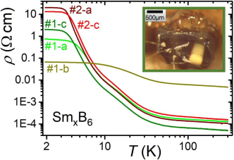
for STM measurements) on the sample properties. To this end, Fig. 1 compares of samples #1 and #2 before denominated “-a”, as-grown) and after cleaving and STM investigation denominated “-c”, cleaved, see inset for cleaved surface of sample #1 with contacts attached). Clearly, for sample #2 there is no significant change. For sample #1 (with refined stoichiometry further away from 1:6 compared to sample #2) an increase of over more than four orders of magnitude upon cooling is only observed after cleaving, curve #1-c in Fig. 1. We speculate that the off-stoichiometry of our samples may influence the surface (and contact) quality in the as-grown case, curve #1-a.
In one case, a significantly smaller increase of resistivity was found, curve #1-b. Closer microscopic inspection revealed a bending of the cleaved, tiny sample after dismounting from our STM sample holder and mounting for transport measurements. Such bending may result in a strained sample. For SmB6 under strain, a considerably reduced increase of resistance with cooling and a higher temperature below which the surface state dominates electrical transport was reported [48]. Indeed, the approach to a low- saturation of appears at higher temperature, around 8 K, and is significantly enlarged at room temperature.
III.3 STM on sample #1
As was reported before [49, 35, 38, 36, 37] large atomically resolved surface areas are rarely observed on pristine SmB6 and typically have to be searched for extendedly. Finding a flat, clean area appears to be slightly easier in case of SmxB6 with nominal 1 indicating that some defects are present in our Sm-deficient samples and promote cleavage. This observation is in line with a reported decrease of hardness of SmxB6 as decreases [13] and the recent suggestion [23] that these defects are line defects.
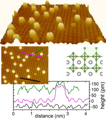
An atomically resolved topography over an area of nm2 of sample #1 is presented in Fig. 2(a). Despite some defects, two flat areas can be distinguished which are separated by a step edge. Its height of about 0.21 nm can be inferred from the pink line scan in Fig. 2(b) taken along the line of similar color in (a). The distances between corrugations conforms to the lattice constant and hence, terminations are observed within both flat areas I and II corresponding to either Sm or B(1)/B(6) surfaces. At first glance, the observed step height of about 0.21 nm conforms well with the expected height difference between Sm and B(2)-(5) terminations (see inset of Fig. 2(b) for B notations). However, such an assignment would involve different terminations (Sm vs. broken B octahedra) and hence, would call for different appearances and arrangements of the corrugations on surfaces I and II (including the so-called doughnuts [32]). In contrast, we observe similar heights and distances of the corrugations on both terraces. Assuming the flat surface areas I and II coincide with B(6) and B(1) terminations, respectively, a step height of 0.248 nm is expected. This value exceeds the measured step height by almost 20%. We note that Fig. 2(a) was obtained in dual bias mode, mV without noticeable difference between these -values.
To scrutinize the step further, the height maxima (marked by ) within area I and II along the pink line were analyzed separately. Assuming constant distances within each one of the terraces yields nm and nm, deviating less than 4% from . Using these -values, the expected atomic positions can be interpolated (marked by ) which deviate in lateral position from the measured height maxima by less then 1% of . This accuracy allows for an extrapolation of the

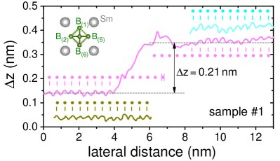
expected atomic positions into the region of the step, i.e. beyond the observable height maxima. In order to estimate the error in our extrapolation, additional line scans on both areas were evaluated (green and light blue line scans) yielding nm and nm. This spread of the -values is included in the error bar ( nm) of the extrapolated atomic positions, see the right-most pink marker of surface I. Within the error of this extrapolation the atomic positions overlap without offset suggesting a certain crystalline continuity in the present field of view. All this affirms that the clean surface areas represent topographies as expected from largely undisturbed crystalline SmB6 without indication for considerable Sm deficiency. The latter is in accord with our findings from XRD.
To gain further insight, zoomed-in areas on either side of the step seen in Fig. 2(a) are presented in Fig. 3(a)–(d). These images were acquired in dual-bias mode, V, allowing for direct comparison of the different -values. As shown for two line scans in Fig. 3(f), the apparent height difference due to the different is less than 10 pm. While the undisturbed lattice regions appear little influenced by , the defects are slightly more pronounced for negative V indicating more negatively charged defects with respect to their surroundings. This, together with the small total height of the defect, rules out a Sm adatom generating this defect. The defect may be caused by either lattice imperfections within or
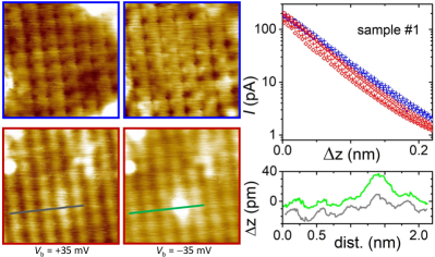
below the surface, or B atoms/cluster resulting from the cleaving process. We note that there is no contrast reversal observed for the -values used here, neither within the lower area I nor the upper area II.
Surfaces are characterized by their work functions . A related parameter, the tunneling barrier height , can be studied by measuring the tunneling current in dependence on tip-sample distance . In clean cases, can be estimated from with , where is the bare electron mass and . Here, is the tip work function. A few vs. -curves are presented in Fig. 3(e) taken on numerous defect-free spots on both surfaces. The barrier heights from the lower surface I (red markers) range between 5.8 eV 6.7 eV, while on the upper surface (blue markers) 4.5 eV 5.4 eV. Albeit there appears to be a difference in the barrier heights within the two surface areas, the total range of is remarkably close to the one obtained on B-terminated EuB6 [38]. Moreover, our range of is considerably smaller than the one reported in [35], possibly due to the much larger clean areas investigated. Specifically, the local barriers heights for clean areas were reported to be of order 4 eV [35], while our observations indicate somewhat larger values. According to Ref. 35, a small work function of 2 eV is expected for Sm-terminated surfaces, a value close to 2.7 eV for pure Sm [50], whereas on B-terminated surfaces it should be at least twice as high. The latter is in line with pure B (4.45 eV, [50]) and an early report on SmB6 with very little Sm in the surface layer (4.2 eV, [51]) as well as more recent angle-resolved photoemission
measurements (4.5 eV, [52]). Although we can only measure , rather than , these results support an assignment of both surfaces I and II to B-terminations, in line with our earlier results [10, 49, 38].
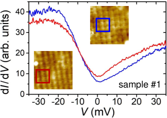
To further support this assignment, STS was conducted within both areas. As evidenced by Fig. 4, there is little difference between the spectra on both areas. While the prominent peak at around mV observed on clean areas and at lower [33, 35] is absent, they exhibit the reduced local density of states near typical of the Kondo hybridization in SmB6. In addition, a broad, yet moderate, hump at around mV is observed [34, 35, 37]. The Kondo hybridization [53] in SmB6 allows for co-tunneling into Sm 4 states and the conduction band that can give rise to a much more pronounced peak at this energy [31, 32, 10, 33, 35, 18, 37]. The small hump then indicates very little tunneling into the Sm 4 states [10, 35]. This reinforces our finding above that both surfaces I and II are likely B terminated. In addition, it was suggested that a maximum in at mV may result from a local doping effect due to boron clusters on the surface [35] which is in line with our assignment of the surface defects to B. Note also that the Sm-deficiency of this sample #1 is likely supportive in establishing these surface properties.
Figure 5(a) presents another clean surface area which exhibits some defects similar to those reported as doughnuts [32]. However, their origin appears to be different from [32] for two reasons: i) the height scans along a 100 direction, Fig. 5(c), reveal two protrusions almost a lattice constant apart. ii) individual doughnuts are observed exclusively. The center of the doughnuts are located on top of dents of the underlying lattice. This positioning, along with the central dent of the doughnuts [clearly seen in Fig. 5(b)], suggests that the defects are not caused by single Sm-atoms on top of a B-termination or vice versa. Rather, they are likely made up of several (conceivably four) B(6) atoms [cf. side view Fig. 5(d)]
forming a round structure, as nicely seen in the 3-dimensional topography Fig. 5(a). This is supported by their apparent height [about 130 pm, magenta line scan in Fig. 5(c)] which is near the inter-octahetral B-distance. Moreover, the size of the doughnuts, both along the 100 and the 110 direction, render a pentaboride cluster on the surface unlikely. Note that the off-stoichiometry of sample #1 makes excess B on the surface likely. Nonetheless, it remains unclear why an apparently invariable number of B-atoms may form such doughnut structures. We speculate that this results from the energetically high impact of the cleaving process. It is worth noting that there are similarities to the topographies presented in [32, 35] albeit with a much higher defect density there.
A revealing type of defect is presented in Fig. 6. The most common
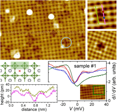
defect in Fig. 6(a) is a cross-like dent, see blue circle. The zoomed view of a different area, Fig. 6(b), clearly reveals that four atoms in a square arrangement of size are shifted lower into the surface by about 10 – 15 pm, cf. line scans in Fig. 6(d). It is important to note here that this type of defect is fairly regularly encountered on surfaces of Sm-deficient samples. In contrast, on stoichiometric SmB6, for which we have reported topographies of 24 cleaves [38], we only found one matching topography, presented in Fig. 6(f). This statistics makes a link between Sm-deficiency and the occurrence of these defects likely. In particular, a missing Sm atom in a sub-surface layer, which may easily be present in the Sm-deficient samples, may cause the four adjacent B6-octahedra within the top layer to slightly rearrange [in the side view, Fig. 6(c), the missing Sm is marked by , adjacent octahedra in the top layer are shaded green]. Within the field of view of Fig. 6(a) there are about 14 such defects. If they are all indeed due to missing Sm-atoms, about 3.4% of Sm would be absent in this particular layer, which is around twice as much as statistically expected. However, as a cleave certainly takes place at structurally weakened positions, such a deviation is conceivable.
By comparison [10, 38], the topographies presented in Fig. 6(a) and (f) represent B-terminated surfaces, as schematically depicted in Fig. 6(c). In this case, defects (missing atoms) on B(6) or B(2)-(5) sites should result in single or, possibly, double dents. Moreover, the spectra obtained at the defect side, red and blue line in Fig. 6(e), as well as on a cleaner spot of the same sample (green line and inset) support the assignment to a B-terminated surface. The possible tunneling into Sm 4 states as well as the conduction band results in a co-tunneling phenomenon. In the simple Fano picture [54, 55], the tunneling conductance can be described by
| (1) |
where is the resonance width and the position in energy relative to may be influenced by the two tunneling channels. Importantly, the asymmetry parameter depends on the ratio of tunneling probabilities into the 4 states vs. into the conduction band, and on the particle-hole asymmetry of the conduction band [56]. While a peak at small negative bias voltage [10, 32, 33, 35, 18, 37] indicates tunneling into 4 states, we only observe a small hump around mV. Fits to eq. 1 (blue dashed line) yield () for the red (blue) spectrum in Fig. 6(e), i.e. very little tunneling into the 4 states. For comparison, on the clean surface area shown in the inset of Fig. 6(e), in good agreement with [10]. We speculate that the lower -value in the Sm-deficient sample is related to the missing Sm. In addition, the fit to the spectrum on a clean side works nicely, while being considerably less reliable at the defect. This may indicate a less-developed Kondo hybridization at the defect site. Such a conjecture is supported by the resonance widths: fitting the spectrum of the undisturbed area (green line and black dashed line) yields 15.1 meV in line with earlier results [9, 52, 10], while it appears somewhat reduced within the defect (red dashed line: 12.9 meV; blue: 13.4 meV). Hence, the hybridization gap is reduced at these defect sites. It is also important to note that the trend we observed for the position of the hump near mV agrees well with the report by Sun et al. [35]: The peak moves to more negative energies and gets less pronounced in height if less clean positions are investigated. Also, there appears to be a small shift of the minimum in dd from towards slightly negative energies at surface areas with impurities and/or adatoms, in line with data presented in [35].
III.4 STM on sample #2
While the nominal Sm deficiency of samples #2 is more pronounced compared to #1, the refined Sm occupancy is very close to unity, see Tab. 1. In line with the latter and as exemplary shown in Fig. 7, atomically flat surface areas with only a surprisingly small number of defects can be found on sample #2, just as rarely as on pristine SmB6. These topographies are consistent with () surface terminations encountered on stoichiometric SmB6. While the off-stoichiometry of our samples SmxB6 certainly influences their cleaving process (in accord with a faster polishing [13]), it appears it does not prevent the SmB6 to form over reasonably large areas, similar to our observations on sample #1. However, as the cleave likely proceeds along crystalline defects and may leave the pristine SmB6 intact, we refrain from any statistics of how much of the surface area might point toward an underlying little-disturbed SmB6 phase. Note that the very faint inhomogeneity (of a few lattice constants in extend) below the atomic protrusions seen within the clean
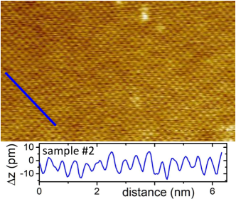
() surface of sample #2 is also reminiscent to observations on clean SmB6 surfaces [10, 49, 18]. So far, such inhomogeneities were only encountered at temperatures around 5 K or above, but not below 2 K, which may indicate a not completely formed conducting surface state at K.
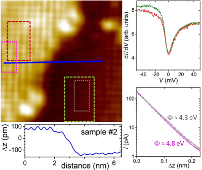
To further scrutinize the above assumption of reasonably large SmB6 regions again a step edge is investigated. Atomic resolution within the terraces indicate terminations separated by a step of about 240 pm in height, see Fig. 8(b). The spectra obtained within clean areas of these two terraces are very similar, with minor differences on the negative bias side. The Fano fits (dashed lines in Fig. 8(c)) yield 16.6 meV (15.7 meV) for the red (green) spectrum, in good agreement with results on SmB6 and clean surface areas of sample #1, indicating a well-developed hybridization gap. The -values are small, and 0.34, with the smaller one on the upper terrace (red spectrum) indicating suppressed tunneling into the Sm -states. In addition, the barrier heights are similar on both terraces, 4.8 eV and 4.3 eV, see Fig. 8(d). Taken together, we surmise that both terraces of sample #2 in Fig. 8(a) depict surfaces of the SmB6 phase, likely with B-termination. The upper (left) terrace would then correspond to the B(1)-surface encountered also on SmB6, while the lower one (right) may be a B(6)-surface. In this case, the expected step height is 0.248 nm, in good agreement with our measurements. Interestingly, such an assignment could even account for the apparent lesser height of the corrugations on the lower B(6)-terrace compared to the upper B(1)-region, Fig. 8(b).
A B(6)-surface has been considered unlikely based on surface energy calculations [35]. On the other hand, the cluster surfaces favored by these calculations seem inconsistent with the majority of the topographies observed here. It should be kept in mind, however, that the Sm-deficiency of our samples most likely influences the samples’ cleavage behavior; they cleave more easily compared to pristine SmB6 samples. This is further corroborated by the observation of a new type of defect as well as a new surface
reconstruction on surfaces of sample #2, which were not encountered on any of the more than 30 cleaved SmB6 surfaces [38]. Taken together, it appears the surface energy is only one of the parameters determining the cleaved surfaces, and may even be changed with respect to pure SmB6.
IV Discussion
Interestingly, the vast majority of atomically resolved surface topographies point to a seemingly undisturbed SmB6 surface structure, as clearly shown in Fig. 7. This finding is consistent with our XRD results. Albeit the topographies presented in Figs. 5 and 6 highlight defects specific to SmxB6 with (i.e. which are not or very rarely encountered on stoichiometric SmB6 surfaces), the underlying topography away from defects appears highly similar to those found on SmB6 (see, e.g. Ref. 38). In fact, atomically resolved surface areas were found somewhat more easily on Sm-deficient samples in comparison to stoichiometric SmB6, even though extensive search was still required. Possibly related to this issue, a step edge as presented in Fig. 2 could so far only be found on one Sm-deficient sample of batch #1. Given the step height and the properties of the adjacent surfaces, it is consistent with a line defect. We note here that, as STM topography only depicts the two-dimensional sample surface, we cannot distinguish whether these observed defects derive from grain boundaries or dislocations. Despite extensive search, pristine SmB6 (more than thirty cleaves) and samples of batch #2 did not reveal such a step edge.
Thermodynamically, the Sm:B solution has a large negative enthalpy of mixing at the 1:6 composition. Therefore, for flux-grown samples an actual composition of SmB6 can be expected. Nonetheless, modified material properties of flux-grown SmxB6 have been reported for , e.g. in Hall measurements [47] and microhardness [13]. Together with the observations of line defects (Fig. 2) and a modified cleaving behavior of the Sm-deficient samples (SmxB6 samples with require much less force for cleaving compared to those with ) we speculate that the off-stoichiometry of Sm and B in the flux results in an increased granularity of the samples while the SmB6 stoichiometry is rather closely preserved within the grains.
The majority of the surfaces discussed here are B-terminated. In this respect it is worth noting that the different reports agree on their assignment of the B-terminated surfaces [10, 31, 32, 35, 18, 37, 38]. Our observation of a cross-like defect on sample #1, Fig. 6 further confirms this assignment. In contrast, the Sm-terminated and the reconstruction are still under debate. So far, we could not unambiguously identify a Sm-terminated surface on Sm-deficient samples. However, we observed a new type of surface reconstruction in one instance (therefore, it is not presented here), which we tentatively assigned ()R45∘. Apparently, the SmB6 structure is preserved locally, while an overall, crystallite-like structure prevails due to the Sm-deficiency.
The observed barrier heights on our Sm-deficient samples are mostly around 5 eV, in good agreement with reports on pristine SmB6 [35] and even EuB6 [38]. For a Sm-terminated surface, a very low work function of order 2 eV is predicted [35]. This should be kept in mind since tunneling is limited to , i.e. the bias voltage should not exceed a few tenths of one V.
It is interesting to note that, within clean areas of likely B-termination, the resonance width is about 15 – 16 meV, in good agreement with results on pure SmB6 samples [10, 35]. This value is somewhat reduced at defects, see Fig. 6(e). Spectra obtained at small spots between B-clusters exhibited also a reduction in gap size [35]. This indicates that the electronic properties of Sm-deficient samples, in particular the hybridization gap, are globally very similar to SmB6, and influenced only locally by defects or off-stoichiometry.
As discussed above, section III.2, transport measurements were conducted on one bent sample #1. The concomitantly increased at room temperature might be explained, according to [48], by an increased Sm valence with tensile strain, which enhances scattering in the Sm 4 channel, and stronger hybridization between - and -orbitals. STS taken beforehand on this surface could nicely be fit by eq. (1) with -values as large as 0.83, which is larger than any value we obtained on B-terminated surfaces so far [10, 33] (fits yielded 14.6 meV 16.7 meV). However, at present we cannot directly correlate this observation with the bending of the sample.
V Conclusion
Macroscopic and microscopic (down to the atomic level) studies were combined on the same Sm-deficient samples SmxB6 with nominal deficiencies up to 25%, i.e. 0.75. Despite this high nominal Sm deficiency, the SmB6 structure in the flux-grown samples remains strikingly stable such that the hybridization gap and the low-temperature surface conductance appear not significantly altered from pure SmB6, an observation supporting a recently reported protection of the SmB6 transport gap against disorder [13]. The Sm vacancies do not disturb the global, macroscopic properties of SmB6, but rather induce crystallographic defects and locally reduce the hybridization gap at these defects. The STM topographies are in good agreement with the XRD results: on sample #2, for which the refined composition is closer to the 1:6 stoichiometry than for sample #1 (see Tab. 1), we were able to find large areas with a smaller number of defects (e.g. Fig. 7) compared to our topographies on sample #1. We also note that for SmxB6 with , XRD did not reveal any other phase than SmB6.
Acknowledgments
Work at Los Alamos National Laboratory was performed under the auspices of the U.S. Department of Energy, Office of Basic Energy Sciences, Division of Materials Science and Engineering. ZF acknowledges support from the LANL G. T. Seaborg Institute. Funding by the German Research Foundation (DFG) through grant WI 1324/5-1 is gratefully acknowledged.
References
- Hasan and Kane [2010] M. Z. Hasan and C. L. Kane, Rev. Mod. Phys. 82, 3045 (2010).
- Rachel [2018] S. Rachel, Rep. Prog. Phys. 81, 116501 (2018).
- Dzero et al. [2010] M. Dzero, K. Sun, V. Galitski, and P. Coleman, Phys. Rev. Lett. 104, 106408 (2010).
- Takimoto [2011] T. Takimoto, J. Phys. Soc. Jpn. 80, 123710 (2011).
- Li et al. [2020] L. Li, K. Sun, C. Kurdak, and J. W. Allen, Nat. Rev. Phys. 2, 463 (2020).
- Rosa and Fisk [2020] P. F. S. Rosa and Z. Fisk, Bulk and surface properties of SmB6. (2020), arXiv:2007.09137.
- Wolgast et al. [2013] S. Wolgast, C. Kurdak, K. Sun, J. W. Allen, D.-J. Kim, and Z. Fisk, Phys. Rev. B 88, 180405(R) (2013).
- Kim et al. [2013] D. J. Kim, S. Thomas, T. Grant, J. Botimer, Z. Fisk, and J. Xia, Sci. Rep. 3, 3150 (2013).
- Zhang et al. [2013] X. Zhang, N. P. Butch, P. Syers, S. Ziemak, R. L. Greene, and J. Paglione, Phys. Rev. X 3, 011011 (2013).
- Rößler et al. [2014] S. Rößler, T.-H. Jang, D. J. Kim, L. H. Tjeng, Z. Fisk, F. Steglich, and S. Wirth, Proc. Natl. Acad. Sci. USA 111, 4798 (2014).
- Wolgast et al. [2015] S. Wolgast, Y. S. Eo, T. Öztürk, G. Li, Z. Xiang, C. Tinsman, T. Asaba, B. Lawson, F. Yu, J. W. Allen, et al., Phys. Rev. B 92, 115110 (2015).
- Syers et al. [2015] P. Syers, D. Kim, M. Fuhrer, and J. Paglione, Phys. Rev. Lett. 114, 096601 (2015).
- Eo et al. [2019] Y. S. Eo, A. Rakoski, J. Lucien, D. Mihaliov, C. Kurdak, P. F. S. Rosa, and Z. Fisk, Proc. Natl. Acad. Sci. USA 116, 12638 (2019).
- Xu et al. [2014] N. Xu, P. K. Biswas, J. H. Dil, R. S. Dhaka, G. Landolt, S. Muff, C. E. Matt, X. Shi, N. C. Plumb, M. Radović, et al., Nat. Commun. 5, 4566 (2014).
- Suga et al. [2014] S. Suga, K. Sakamoto, T. Okuda, K. Miyamoto, K. Kuroda, A. Sekiyama, J. Yamaguchi, H. Fujiwara, A. Irizawa, T. Ito, et al., J. Phys. Soc. Jpn. 83, 014705 (2014).
- Thomas et al. [2016] S. Thomas, D. J. Kim, S. B. Chung, T. Grant, Z. Fisk, and J. Xia, Phys. Rev. B 94, 205114 (2016).
- Jiao et al. [2018] L. Jiao, S. Rößler, D. Kasinathan, P. F. S. Rosa, C. Guo, H. Yuan, C.-X. Liu, Z. Fisk, F. Steglich, and S. Wirth, Sci. Adv. 4, eaau4886 (2018).
- Pirie et al. [2020] H. Pirie, Y. Liu, A. Soumyanarayanan, P. Chen, Y. He, M. M. Yee, P. F. S. Rosa, J. D. Thompson, D.-J. Kim, Z. Fisk, et al., Nat. Phys. 16, 52 (2020).
- Zhu et al. [2013] Z.-H. Zhu, A. Nicolaou, G. Levy, N. P. Butch, P. Syers, X. F. Wang, J. Paglione, G. A. Sawatzky, I. S. Elfimov, and A. Damascelli, Phys. Rev. Lett. 111, 216402 (2013).
- Hlawenka et al. [2018] P. Hlawenka, K. Siemensmeyer, E. Weschke, A. Varykhalov, J. Sánchez-Barriga, N. Y. Shitsevalova, A. V. Dukhnenko, V. B. Filipov, S. Gabáni, K. Flachbart, et al., Nat. Commun. 9, 517 (2018).
- He et al. [2017] H. He, L. Miao, E. Augustin, J. Chiu, S. Wexler, S. A. Breitweiser, B. Kang, B. K. Cho, C.-H. Min, F. Reinert, et al., Phys. Rev. B 95, 195126 (2017).
- Sen et al. [2020] S. Sen, N. S. Vidhyadhiraja, E. Miranda, V. Dobrosavljević, and W. Ku, Phys. Rev. Research 2, 033370 (2020).
- Eo et al. [2020] Y. S. Eo, A. Rakoski, S. Sinha, D. Mihaliov, W. T. Fuhrman, S. R. Saha, P. F. S. Rosa, Z. Fisk, M. Ciomaga Hatnean, G. Balakrishnan, et al., Bulk transport paths through defects in floating zone and Al flux grown SmB6. (2020), arXiv:2011.08923.
- Lutz et al. [2016] P. Lutz, M. Thees, T. R. F. Peixoto, B. Y. Kang, B. K. Cho, C.-H. Min, and F. Reinert, Philos. Mag. 96, 3307 (2016).
- Utsumi et al. [2017] Y. Utsumi, D. Kasinathan, K.-T. Ko, S. Agrestini, M. W. Haverkort, S. Wirth, Y.-H. Wu, K.-D. Tsuei, D.-J. Kim, Z. Fisk, et al., Phys. Rev. B 96, 155130 (2017).
- Sundermann et al. [2018] M. Sundermann, H. Yavas, K. Chen, D. Kim, Z. Fisk, D. Kasinathan, M. Haverkort, P. Thalmeier, A. Severing, and L. Tjeng, Phys. Rev. Lett. 120, 016402 (2018).
- Lu et al. [2013] F. Lu, J. Zhao, H. Weng, Z. Fang, and X. Dai, Phys. Rev. Lett. 110, 096401 (2013).
- Antonov et al. [2002] V. N. Antonov, B. N. Harmon, and A. N. Yaresko, Phys. Rev. B 66, 165209 (2002).
- Kang et al. [2015] C.-J. Kang, J. Kim, K. Kim, J. Kang, J. D. Denlinger, and B. I. Min, J. Phys. Soc. Jpn. 84, 024722 (2015).
- Kirchner et al. [2020] S. Kirchner, S. Paschen, Q. Chen, S. Wirth, D. Feng, J. D. Thompson, and Q. Si, Rev. Mod. Phys. 92, 011002 (2020).
- Yee et al. [2013] M. M. Yee, Y. He, A. Soumyanarayanan, D.-J. Kim, Z. Fisk, and J. E. Hoffman, Imaging the Kondo insulating gap on SmB6. (2013), arXiv:1308.1085.
- Ruan et al. [2014] W. Ruan, C. Ye, M. Guo, F. Chen, X. Chen, G.-M. Zhang, and Y. Wang, Phys. Rev. Lett. 112, 136401 (2014).
- Jiao et al. [2016] L. Jiao, S. Rößler, D. J. Kim, L. H. Tjeng, Z. Fisk, F. Steglich, and S. Wirth, Nat. Commun. 7, 13762 (2016).
- Miyamachi et al. [2017] T. Miyamachi, S. Suga, M. Ellguth, C. Tusche, C. M. Schneider, F. Iga, and F. Komori, Sci. Rep. 7, 12837 (2017).
- Sun et al. [2018] Z. Sun, A. Maldonado, W. S. Paz, D. S. Inosov, A. P. Schnyder, J. J. Palacios, N. Y. Shitsevalova, V. B. Filipov, and P. Wahl, Phys. Rev. B 97, 235107 (2018).
- Matt et al. [2020] C. E. Matt, H. Pirie, A. Soumyanarayanan, Y. He, M. M. Yee, P. Chen, Y. Liu, D. T. Larson, W. S. Paz, J. J. Palacios, et al., Phys. Rev. B 101, 085142 (2020).
- Herrmann et al. [2020] H. Herrmann, P. Hlawenka, K. Siemensmeyer, E. Weschke, J. Sánchez-Barriga, A. Varykhalov, N. Y. Shitsevalova, A. V. Dukhnenko, V. B. Filipov, S. Gabáni, et al., Adv. Mater. 32, 1906725 (2020).
- Wirth et al. [2021] S. Wirth, S. Rößler, L. Jiao, M. V. Ale Crivillero, P. F. S. Rosa, and Z. Fisk, Phys. Status Solidi B 258, 2000346 (2021).
- Rosa and Fisk [2018] P. F. S. Rosa and Z. Fisk, in Crystal Growth of Intermetallics, edited by P. Gille and Y. Grin (Berlin, Boston: De Gruyter, 2018), pp. 49–60.
- Phelan et al. [2016] W. A. Phelan, S. M. Koohpayeh, P. Cottingham, J. A. Tutmaher, J. C. Leiner, M. D. Lumsden, C. M. Lavelle, X. P. Wang, C. Hoffmann, M. A. Siegler, et al., Sci. Rep. 6, 20860 (2016).
- Gabáni et al. [2016] S. Gabáni, M. Orendáč, G. Pristáš, E. Gažo, P. Diko, and S. Piovarči, Philos. Mag. 96, 3274 (2016).
- Valentine et al. [2016] M. E. Valentine, S. Koohpayeh, W. A. Phelan, T. M. McQueen, P. F. S. Rosa, Z. Fisk, and N. Drichko, Phys. Rev. B 94, 075102 (2016).
- [43] Full sets of supplementary crystallographic data for this paper have been deposited with the joint CCDC and FIZ Karlsruhe deposition service. The data can be obtained free of charge from The Cambridge Crystallographic Data Centre via www.ccdc.cam.ac.uk/structures citing deposition numbers CSD 2073128 - 2073130.
- [44] Omicron Nanotechnology GmbH, Taunusstein (Germany).
- Gheidi et al. [2019] S. Gheidi, K. Akintola, K. S. Akella, A. M. Côté, S. R. Dunsiger, C. Broholm, W. T. Fuhrman, S. R. Saha, J. Paglione, and J. E. Sonier, Phys. Rev. Lett. 123, 197203 (2019).
- Orendáč et al. [2017] M. Orendáč, S. Gabáni, G. Pristáš, E. Gažo, P. Diko, P. Farkašovský, A. Levchenko, N. Shitsevalova, and K. Flachbart, Phys. Rev. B 96, 115101 (2017).
- Stankiewicz et al. [2019] J. Stankiewicz, M. Evangelisti, P. F. S. Rosa, P. Schlottmann, and Z. Fisk, Phys. Rev. B 99, 045138 (2019).
- Stern et al. [2017] A. Stern, M. Dzero, V. M. Galitski, Z. Fisk, and J. Xia, Nat. Mater. 16, 708 (2017).
- Rößler et al. [2016] S. Rößler, L. Jiao, D. J. Kim, S. Seiro, K. Rasim, F. Steglich, L. H. Tjeng, Z. Fisk, and S. Wirth, Philos. Mag. 96, 3262 (2016).
- Michaelson [1977] H. B. Michaelson, J. Appl. Phys. 48, 4729 (1977).
- Aono et al. [1979] M. Aono, R. Nishitani, C. Oshima, T. Tanaka, E. Bannai, and S. Kawai, Surf. Sci. 86, 631 (1979).
- Neupane et al. [2013] M. Neupane, N. Alidoust, S.-Y. Xu, T. Kondo, Y. Ishida, D. J. Kim, C. Liu, I. Belopolski, Y. J. Jo, T.-R. Chang, et al., Nat. Commun. 4, 2991 (2013).
- Wirth and Steglich [2016] S. Wirth and F. Steglich, Nat. Rev. Mat. 1, 16051 (2016).
- Fano [1961] U. Fano, Phys. Rev. 124, 1866 (1961).
- Schiller and Hershfield [2000] A. Schiller and S. Hershfield, Phys. Rev. B 61, 9036 (2000).
- Figgins and Morr [2010] J. Figgins and D. K. Morr, Phys. Rev. Lett. 104, 187202 (2010).